Optics and Photonics Journal
Vol.3 No.4A(2013), Article ID:35658,5 pages DOI:10.4236/opj.2013.34A007
The Effect of Laser Sintering Process Parameters on Cu Nanoparticle Ink in Room Conditions
1Department of Electronics and Communications Engineering, Tampere University of Technology, Tampere, Finland
2Center of Microscopy and Nanotechnology CNMT, University of Oulu, Oulu, Finland
Email: eerik.halonen@tut.fi
Copyright © 2013 Eerik Halonen et al. This is an open access article distributed under the Creative Commons Attribution License, which permits unrestricted use, distribution, and reproduction in any medium, provided the original work is properly cited.
Received April 17, 2013; revised May 31, 2013; accepted June 23, 2013
Keywords: Nanoparticles; Electrical Properties; Laser Processing; Microstructure; Sintering; Thin Films
ABSTRACT
Copper is an interesting material for printed electronics inks because, for example, of its good conductivity and lower raw material price compared to silver. However, post-processing Cu inks is challenging because of non-conductive copper oxide. In this work, inkjet-printed Cu nanoparticle structures were sintered on a polyimide substrate with a continuous-wave 808-nm diode laser. Laser sintering was tested by varying the sintering parameters (optical power and scanning velocity), and the electrical resistance of the samples was measured. A minimum sheet resistance of approx. 90 mΩ/□ was obtained. All tests were run in room conditions. Sintered structures were then analyzed from SEM images. Results showed that laser sintering produces good repeatability, that a scanning velocity increment positively affects the process window, and that multiple sintering cycles do not increase conductivity.
1. Introduction
In the past decade, printed electronics has come under extensive research, and not only printing technologies but also increasingly material development and post processing methods. Furthermore, printed electronics has found applications, for example, in electric paper, RFID tags, and various sensors [1,2]. In addition to contactless performance, inkjet printing, a most agile printing method, harbours possibilities for wide-ranging customization and is thus keenly studied by several research groups around the world [3-5].
Various materials, including conductive, dielectric, and semi-conductive materials, are available as suitable candidates for inkjet printing. A common conductive ink contains metal (e.g., silver, gold, nickel, or copper) nanoparticles surrounded by a thin dispersive material (commonly some polymer) and diluted in one or several solvents. In post-processing, called sintering, solvent and dispergents are removed, and a conductive path is formed across the metal particles by applying heat to the ink structure, usually by oven sintering [6,7]. Silver has been used most frequently because of its low resistivity and simple handling in post processing. However, recentlycopper, a less expensive raw material, has been generating interest but has also been posing post-processing challenges because of non-conductive copper oxide. An Ag ink can be sintered in an oven, but a Cu ink needs an inert atmosphere or an alternative approach to sintering. Laser sintering of screen-printed copper paste in nitrogen atmosphere has been demonstrated in a few studies so far [8,9].
In a non-inert atmosphere, nano Cu must be sintered in a very short time. Therefore, Cu ink can be sintered in ambient conditions using the following two techniques: pulsed light [10,11] and laser sintering [12]. In laser sintering, a laser beam scans the ink structure with either the beam or the substrate platform moving. Two laser types, continuous-wave and pulsed lasers, have been successfully used to sinter Ag nanoparticle ink. [13] The advantages of laser sintering over traditional oven sintering are speedy process and possibility to sinter locally. In this study, we discuss on sintering of inkjet-printed Cu nanoparticle ink on a polyimide substrate with an 808-nm continuous-wave diode laser. Tests were run in ambient room conditions instead of an inert atmosphere, different scanning velocities and laser powers were compared, and the repeatability of the process was assessed.
2. Experiments
2.1. Materials and Sample Fabrication
In this test, we used Applied Nanotech, Inc. Cu-IJ70 ink and 50-μm-thick Kapton HN polyimide film [14]. In addition to copper nanoparticles, the ink contained a complex combination of organic solvents, including aliphatic acetate and derivatized glycol ether, combined with a dispersion agent to create an electrostatic repulsion layer on nanoparticles to control agglomeration. According to the manufacturer, the particle size was 50 - 70 nm and the solid content 30 wt%. Polyimide film was chosen because it can withstand laser-irradiation-induced heat stress and thus rapid heating of the copper layer.
Our printing equipment was an inkjet material deposition system (iTi XY MDS2.0) and a drop-on-demand printhead (Dimatix Spectra SE-128) with 128 nozzles creating approx. 30 picoliter droplets. The drop diameter on a 70˚C substrate was about 100 µm. For surface treatment before printing, the substrate was cleaned with isopropanol.
The printed structures were simple straight conductors (example can be seen Figure 1(b)) with measurement pads at both ends. The conductors were of length 40 mm and the squares 1 mm × 1 mm; after printing, the conductors were, on average, of width 300 µm. We used print file of 800 dpi resolution.
2.2. Laser Equipment
We studied laser sintering in ambient room conditions instead of an inert (e.g., nitrogen) atmosphere. The laser used was an 808-nm continuous-wave semiconductor laser HLU35C10x2-808-CB by LissotschenkoMikrooptik (LIMO) with its output power adjustable up to 35 W. The spectral width of the beam was 2.5 nm and the peak wavelength 808.6 nm. A spherical lens with a focal length of 125 mm was used. However, the lens was finally placed 127 mm over the sintering platform for the beam to be slightly off-focus to even out its intensity. The laser spot for sintering was ca. 1.1 mm × 0.4 mm and placed so that the beam’s longer edge was parallel to the sintering direction (x-axis). Based on our experiments, this placement provided ideal sintering results.
The laser diode was installed in a static frame, and the substrate was moved under the laser with a motorized XY-table. An area was sintered by sweeping the substrate under the beam at a steady pacealong the horizontal axis and then moving it alongthe vertical axis in 0.3- mm increments (hatch) after each sweep (Figure 1). The speed of the XY-table was adjustable and a critical variable in our study, the other being the output power of the laser.
2.3. Structural Analysis
The surface of the laser-sintered structures was analyzed with a scanning electrode microscope (SEM). Pictures were taken of the top surface and of sample cross-sections. A Zeiss Ultra-55 FE-SEM (field-emission scanning electron microscope) was used for surface SEM pictures. Conductor cross-sections were made using an FEI Helios
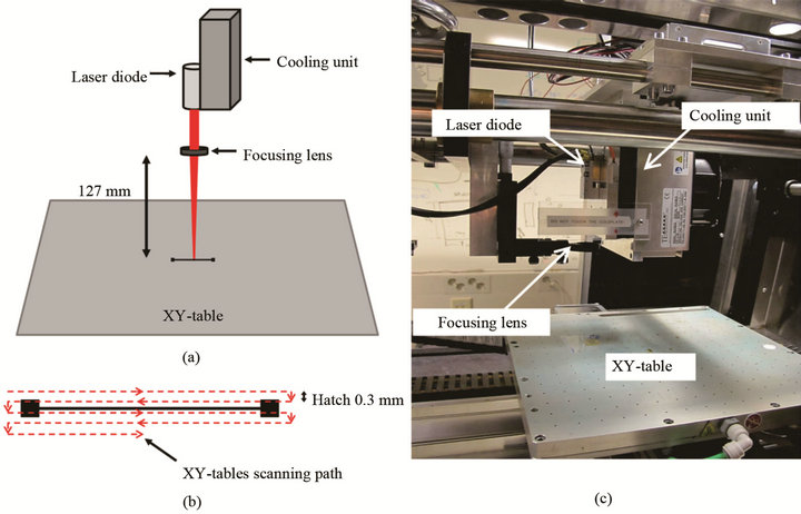
Figure 1. (a) and (c) Laser sintering process setup, and (b) scanning process sequence with 0.3 mm hatch.
Nanolab 600 dualbeam system. A thin layer of platinum (~0.5 µm) was first deposited on the surface as a protective layer with a focused ion beam (FIB). A rough crosssection was then cut from the bulk material using the FIB’s cross-section tool. The cross section surface was then polished with the FIB using a smaller current (i.e., a small beam size). Then images of the cross section surfaces were taken with the Helios 600 dual-beam system SEM.
3. Results and Discussion
Sintered samples were electrically measured with a multimeter with values obtained at an accuracy of 0.1 ohms, which is below 1% of the average resistance value. Figure 2 shows the resistance of Cu conductors after sintering as a function of the laser’s optical power. Four different (50 mm/s, 100 mm/s, 200 mm/s, and 400 mm/s) xy-plate scanning velocities were used. The graphs show that the resistance dropped steeply as the laser’s optical power was increased. After that the resistance stabilized at constant minimum, in this case, below 12 Ω, i.e., 90 mΩ/□. When the optical power was further increased, the copper conductor and the polyimide substrate film under it burned in each case. However, at 400 mm/s velocity this point did not occur because we did not wish to run our laser at close to its maximum power. In the figure, burning is shown as a rapid increment in resistance.
Comparing the graphs of different plate velocities, we can observe thatthe higher the velocity of the XY-plate, the smaller the effect of a constant increment in optical power. This indicates that the power window for good conductivity was wider at high velocities. For example, the window was two times larger at 100 mm/s and at least five times larger at 400 mm/s than at 50 mm/s. High velocities not only shorten the production time but also benefit us when sintering uneven or three-dimensional surfaces, where a fixed laser’s beam focus and thus its optical power vary depending on surface topography. Therefore, at high velocities the process is more tolerant of surface roughness.
The level of sintering copper ink was studied with SEM analysis. Figure 3 shows three sintering stages. Figures 3(a)-(c) are cross-sectional images and Figures 3(d)-(f) are the corresponding images of surfaces. These SEM images are of samples sintered at 50 mm/s velocity and chosen from different points of the resistance-optical power graph such that the first is unsintered, the second sintered at 2.62 Woptical power, and the third at 7.95 W. The first does not conduct, the second has a resistance of 53.7 Ω, and the third has a stable minimum resistance of about 11 - 12 Ω. In the images, the Cu layer is about 1 µm thick.
The pictures show a difference in structural density in different cases. The unsintered sample (Figure 3(a)) is structurally very porous, but it forms markedly dense and solid, i.e., larger grain size, as laser power is increased and conductivity enhances. The SEM images of samples

Figure 2. The resistance of laser sintered samples as a function of the optical power of the laser diode. Four (50 mm/s, 100, mm/s, 200 mm/s, 400 mm/s) scanning velocities were used.
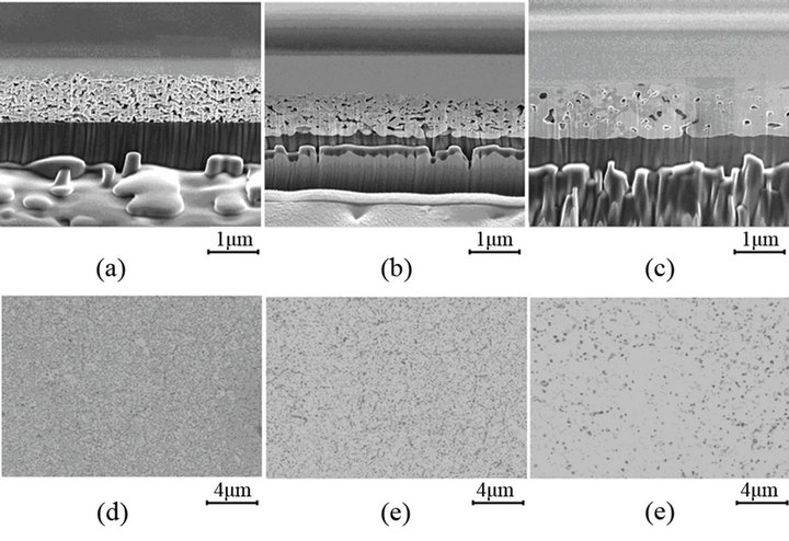
Figure 3. (a)-(c) cross-section and (d)-(f) surface SEM images from laser sintered Cu conductors. Sintering parameters were: for (a) and (d) speed: 50 mm/s, optical power: 0 W; for (b) and (e) speed: 50 mm/s, optical power: 2.62 W; for (c) and (f) speed: 50 mm/s.
sintered at 400 mm/s velocity showed just similar behavior. Interestingly, at every stage the Cu nanoparticle structure looks very homogenous through its whole thickness. Previous studies on oven and Argon plasma sintered silver nanoparticles have shown that the process proceeds from the upper surface of the structure towards the bottom interface between silver and substrate material [6,15]. Theseresults indicate that the conductor structure forms differently in oven and laser sintering.
Repeatability analysis of the sintering process was made. Laser sintering parameters were: XY-table velocity: 200 mm/s, laser diode optical power: 4.5 W. Table 1 shows results obtained when sintering several traces with constant laser sintering parameters. Measurement uncertainty explains most of the variation in the resistance results, though some other process parameters, such as printing quality, played a part.
In addition, we wanted to examine if repetitive laser irradiation cycles at constant optical power and speed could increase conductivity. The idea was to find out if we can achieve equal conductivity by sintering multiple times with a lower laser power than we obtained with higher power values. The tests were made with 100 mm/s and 200 mm/s velocities. However, conductor resistances remained the same regardless of the number of sintering cycles at the same constant optical power and speed.
4. Conclusion
Copper nanoparticle ink was inkjet-printed on polyimide substrate film. After that, the ink was sintered with an 808-nm continuous-wave diode laser in ambient room conditions. Several laser optical power values were used with four different scanning velocities. A sheet resistance of about 90 mΩ/□ was achieved. More importantly, increasing the scanning velocity seemed to widen the la-
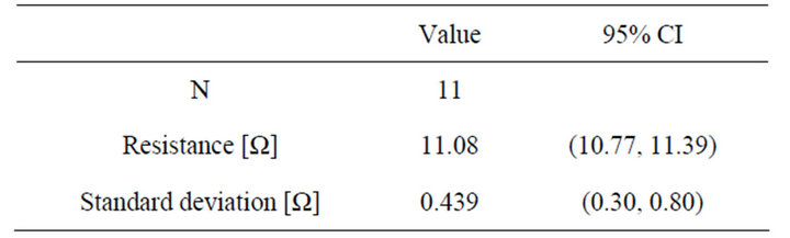
Table 1. Laser sintering repeatability results with fixed parameters. Velocity 200 mm/s and optical power 4.5 W.
ser’s power window for good conductivity, indicating that high velocities may reduce the effect of process variations, such as the altitude variance of surface. The study also shows that laser sintering has good repeatability and that multiple sintering cycles at constant optical power and velocity do not increase conductivity.
5. Acknowledgements
M. Mäntysalo is sponsored by Academy of Finland with grant No. 251882.
REFERENCES
- S. E. Molesa, “Ultra-Low-Cost Printed Electronics,” Technical Report No.UCB/EECS-2006-55, Electrical Engineering and Computer Sciences, University of California at Berkeley, Berkeley, 2006.
- M. A. M. Leenen, V. Arning, H. Thiem, J. Steiger and R. Anselmann, “Printable Electronics: Flexibility for the Future,” Physica Status Solidi (A), Vol. 206, No. 4, 2009, pp. 588-597. doi:10.1002/pssa.200824428
- V. Pekkanen, K. Kaija, M. Mäntysalo, E. Kunnari, J. Niittynen and P. Mansikkamäki, “Functional Fluid Jetting Performance Optimization,” Microelectronics Reliability, Vol. 50, No. 6, 2010, pp. 864-871. doi:10.1016/j.microrel.2010.02.002
- D. Soltman and V. Subramanian, “Inkjet-Printed Line Morphologies and Temperature Control of the Coffee Ring Effect,” American Chemical Society, 2008.
- D. Jang, D. kim and J. Moon, “Influence of Fluid Physical Properties on Ink-Jet Printability,” Langmuir, Vol. 25, No. 5, 2009, pp. 2629-2635. doi:10.1021/la900059m
- E. Halonen, T. Viiru, K. Östman, A. L. Cabezas and M. Mäntysalo, “Oven Sintering Process Optimization for Inkjet-Printed Ag Nanoparticle Ink,” IEEE Transactions on Components, Packaging and Manufacturing Technology, Vol. 3, No. 2, 2013, pp. 350-356. doi:10.1109/TCPMT.2012.2226458
- J. R. Greer and R. A. Street, “Thermal Cure Effects on Electrical Performance of Nanoparticle Silver Inks,” Acta Materia, Vol. 55, No. 18, 2007, pp. 6345-6349.
- M. Joo, B. Lee, S. Jeong and M. Lee, “Laser Sintering of Cu Paste Film Printed on Polyimide Substrate,” Applied Surface Science, Vol. 258, No. 1, 2011, pp. 521-524. doi:10.1016/j.apsusc.2011.08.076
- M. Joo, B. Lee, S. Jeong and M. Lee, “Comparative Studies on Thermal and Laser Sintering for Highly Conductive Cu Films Printable on Plastic Substrate,” Thin Solid Films, Vol. 520, No. 7, 2012, pp. 2878-2883. doi:10.1016/j.tsf.2011.11.078
- H.-S. Kim, S. R. Dhage, D.-E. Shim and H. T. Hahn, “Intense Pulsed Light Sintering of Copper Nanonink for Printed Electronics,” Applied Physics A—Materials Science and Processing, Vol. 97, No. 4, 2009, pp. 791-798. doi:10.1007/s00339-009-5360-6
- J. Ryu, H.-S. Kim and H. T. Hahn, “Reactive Sintering of Copper Nanoparticles Using Intense Pulsed Light for Printed Electronics,” Journal of Electronic Matererials, Vol. 40, No. 1, 2011, pp. 42-50. doi:10.1007/s11664-010-1384-0
- E. Halonen, S. Koskinen, I. Leino, P. Heljo and M. Mäntysalo, “Sintering of Inkjet-Printed Cu-nanoparticle Ink in Ambient Conditions Using a Continuous Wave 808 nm Diode Laser,” MRS Proceedings, Vol. 1529, 2013.
- T. Kumpulainen, J. Pekkanen, J. Valkama, J. Laakso, R. Tuokko and M. Mäntysalo, “Low Temperature Nanoparticle Sintering with Continuous Wave and Pulse Lasers,” Optics and Laser Technology, Vol. 43, No. 3, 2011, pp. 570-576. doi:10.1016/j.optlastec.2010.08.002
- Kapton HN Datasheet. http://www2.dupont.com/Kapton/en_US/assets/downloads/pdf/HN_datasheet.pdf
- I. Reinhold, et al., “US Argon Plasma Sintering of Inkjet Printed Silver Tracks on Polymer Substrates,” Journal of Materials Chemistry, Vol. 19, No. 21, 2009, pp. 3384- 3388. doi:10.1039/b823329b