Journal of Surface Engineered Materials and Advanced Technology
Vol.3 No.3(2013), Article ID:34222,10 pages DOI:10.4236/jsemat.2013.33027
Epitaxial Ge Growth on Si(111) Covered with Ultrathin SiO2 Films
![]()
1A. V. Rzhanov Institute of Semiconductor Physics of SB RAS, Novosibirsk, Russia; 2Novosibirsk State University, Novosibirsk, Russia.
Email: shklyaev@isp.nsc.ru
Copyright © 2013 Alexander A. Shklyaev et al. This is an open access article distributed under the Creative Commons Attribution License, which permits unrestricted use, distribution, and reproduction in any medium, provided the original work is properly cited.
Received May 6th, 2013; revised June 7th, 2013; accepted June 27th, 2013
Keywords: Ge/Si Heterostructures; Epitaxial Growth; Surface Morphology; Scanning Tunneling Microscopy
ABSTRACT
The epitaxial growth of Ge on Si(111) covered with the 0.3 nm thick SiO2 film is studied by scanning tunneling microscopy. Nanoareas of bare Si in the SiO2 film are prepared by Ge deposition at a temperature in the range of 570˚C - 650˚C due to the formation of volatile SiO and GeO molecules. The surface morphology of Ge layers grown further at 360˚C - 500˚C is composed of facets and large flat areas with the Ge(111)-c(2 × 8) reconstruction which is typical of unstrained Ge. Orientations of the facets, which depend on the growth temperature, are identified. The growth at 250˚C - 300˚C produces continuous epitaxial Ge layers on Si(111). A comparison of the surface morphology of Ge layers grown on bare and SiO2-film covered Si(111) surfaces shows a significantly lower Ge-Si intermixing in the latter case due to a reduction in the lattice strain. The found approach to reduce the strain suggests the opportunity of the thin continuous epitaxial Ge layer formation on Si(111).
1. Introduction
Further development of optoelectronics and photonics can be associated with the fabrication of integrated devices based on III-V semiconductors grown on Si substrates [1,2]. The preparation of continuous thin GaAs layers by their growth on the bare Si surfaces is impeded because of the large lattice mismatch (~4%) between GaAs and Si. The growth occurs through the StranskiKrastanov growth mode, leading to the formation of three-dimensional islands. Since the lattice constants of Ge and GaAs are almost equal, Ge or SiGe layers can be used as an intermediate layer between Si and GaAs [3-5]. Moreover, Ge layers on Si improve the performance of integrated Si circuits due to a greater hole mobility in Ge. For these purposes, the preparation of continuous thin Ge layers with good crystalline quality on Si is required.
The Ge growth on Si(111) proceeds through the formation of a Ge wetting layer with the thickness of 2 - 3 bilayers (BL) [6-8]. Further Ge deposition leads to the three-dimensional island formation, the shape and size of which strongly depend on the growth temperature [7,9, 10]. The growth is accompanied by the introduction of threading dislocations into the islands and a dislocation network into the Ge layer at the interface between Ge and Si [11-13]. When the growth temperatures are above 500˚C, the lattice strain causes the significant intermixing of Ge and Si atoms [14-16]. The strain, being most strong at the island edges, induces the formation of deep trenches around large flat islands [17-19]. All these factors prevent the formation of continuous thin Ge layers on Si(111).
Nanocontact epitaxy has been recently proposed to grow continuous layers of semiconductor materials on Si despite the large difference in their lattice constants [20,21]. The method is based on the use of Si surfaces covered with the ultrathin SiO2 film. Ge deposition on such surfaces at rather high temperatures results in the formation of bare Si nanoareas with the size depending on the amount of deposited Ge and temperature [22-25]. The distance between the areas is 7 - 10 nm. The areas of bare Si in the SiO2 film appear due to the reaction of deposited Ge with SiO2 producing the volatile SiO and GeO molecules [22,23]. The bare Si nanoareas serve for the epitaxial growth of semiconductor materials which can form a continuous layer due to the island nucleation and growth over the residuals of the SiO2 film. The nanocontact epitaxy is studied here with respect to revealing the possibility of thin continuous epitaxial Ge layer formation on Si(111) substrates covered with ultrathin SiO2 films. The influence of the technological parameters, such as growth temperature and Ge coverage on the structure and the surface morphology of the grown Ge layers, is examined using scanning tunneling microscopy.
2. Experimental Details
The experiments were carried out in an ultrahigh-vacuum chamber with the base pressure of about 1 × 10⁻¹⁰ Torr. The chamber was equipped with a scanning tunneling microscope (STM) manufactured by Omicron. A Knudsen cell with a BN crucible was used for Ge deposition at the rate from 0.5 to 1.1 BL/min [1 bilayer (BL)  1.44 × 10¹⁵ atoms/cm2] which was calibrated with the STM for the Ge wetting layer growth on the Si(111) surface. After electrochemical etching, the sharp W STM tips were modified by tip apex cut from several sides using the 30 kV Ga ion beam of a separate Zeiss 1540 XB cross beam scanning electron microscope. The opening angle of sharpened STM tips was less than 25˚. The STM images of the surfaces covered with Ge were usually obtained with the sample bias voltage of 2.4 V and the constant current between 3 and 30 pA.
A 10 × 2 × 0.3 mm3 sample was cut from an n-type Si(111) wafer with a miscut angle of < 10' and the resistivity of 5 - 10 Ω·cm. Clean Si surfaces were prepared by flash direct-current heating at 1200˚C. The sample temperature was measured using IMPAC IGA 12 pyrometer. To grow the ultrathin SiO2 film, the sample temperature was set to 400˚C and raised to 550˚C for 10 min after oxygen had been introduced into the chamber at the pressure of 2 × 10⁻⁶ Torr. The SiO2 film, prepared at the similar conditions, was previously investigated to be 0.3 - 0.5 nm thick and mainly composed of silicon dioxide (SiO2) and it also contained Si atoms at different oxidation stages [26]. However, it is named here as the SiO2 film. After the SiO2 film growth, the chamber was pumped to the pressure of ~1 × 10⁻⁹ Torr for 10 min and then the Ge crucible temperature was set to the range from 1110 to 1150˚C. The sample temperature was being maintained for 5 min after finishing the deposition. Image processing and correction software were employed to reduce distortion of the STM images caused by effects of thermal drift of the STM tip against the sample and to obtain statistical characteristics of the surface morphology, such as stereographic projections of surface areas and portions of the areas as a function of their inclination angle with respect to the sample surface.
3. Surface Morphology at a Relatively Small Ge Coverage
The 4 BL Ge deposition on Si(111) covered with the ultrathin SiO2 film results in the appearance of Ge islands, as shown in Figure 1, without the formation of Ge wetting layers. The interaction of Ge with SiO2 occurs through the reaction [22,23]
 (1)
(1)
producing volatile SiO and GeO molecules at temperatures above 430˚C. Reaction (1) has a strong temperature dependence that is characterized by the activation energy of 2 - 3 eV [27]. This leads to the appearance of bare Si surface areas in the SiO2 film. Then other reactions
 and
and
 (2)
(2)
start competing with reaction (1). These are the attachment of deposited Ge atoms to the bare Si areas, giving nucleation and growth of the epitaxial Ge islands. Reactions (2) include the surface diffusion and are characterized by the activation energy of about 1 eV [28].
The density of Ge island arrays and the lateral island size are independent of the growth temperature up to about 570˚C, whereas the density decreases and the lateral size increases with the temperature in the higher temperature range between 570˚C and 650˚C. Figure 2 shows that at 590˚C the island size increases with the increasing Ge coverage so that, at a coverage of 3 BL, the separation between some islands disappears and the islands start to merge. This causes the appearance of large variations in the island size under the further Ge deposition [Figure 3(a)]. At higher temperatures the larger islands continue to grow, while smaller islands can decrease in size and even disappear [Figure 3(b)]. This feature looks like Oswald ripening that occurs under the lattice strain, which increases with Ge coverage.
The temperature dependence of the Ge island formation can be explained by a large difference in the activetion energies of reactions (1) and (2). The STM data suggest that the rate of reaction (2) is substantially higher
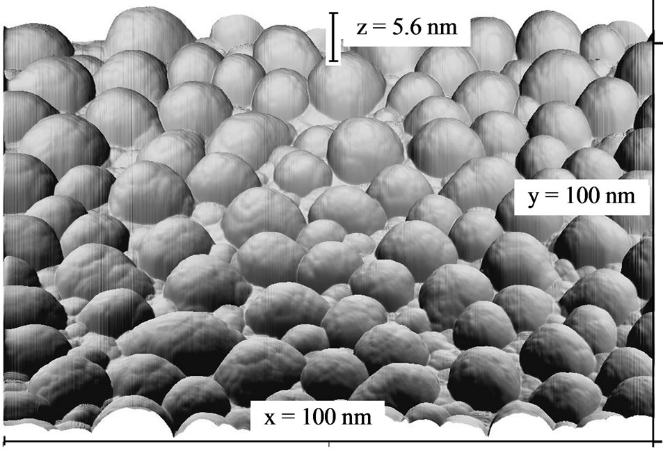
Figure 1. STM image of the oxidized Si(111) surface covered with 4 BL of Ge at 450˚C.
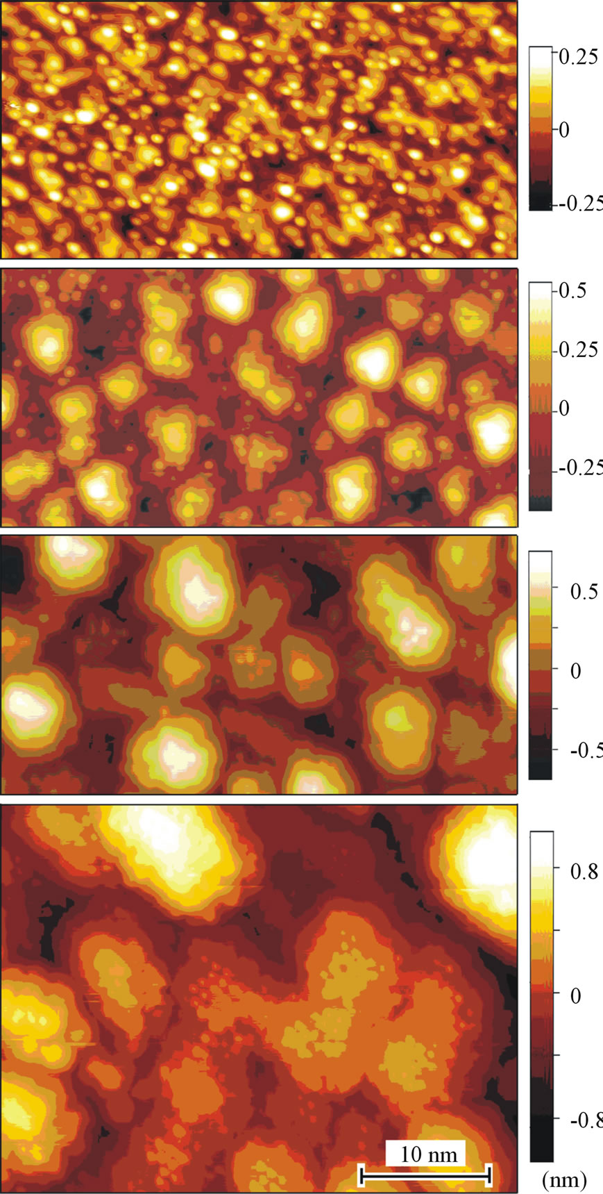
Figure 2. STM images of the oxidized Si(111) surface (a) before and after Ge deposition at the amount of (b) 1, (c) 2 and (d) 3 BL at 590˚C. The images have the same lateral scale.
than the rate of reaction (1) in the low temperature range up to about 590˚C. So, the reaction (1) acts only at the initial deposition stage until bare Si areas appear. Ge adatoms then start to preferably attach to these areas and form Ge islands by means of reaction (2), whereas reaction (1) is suppressed. As a result, Ge islands laterally grow over the residuals of the SiO2 film. The rate of reaction (1) increases stronger with the increasing temperature due to the greater activation energy and becomes comparable to the rate of reaction (2) at temperatures above 590˚C at which the SiO2 decomposition occurs simultaneously with the island growth. This leads to the formation of larger areas of direct contacts between the Si substrate and the growing Ge islands. At the same time, the Ge islands attain a larger lateral size and
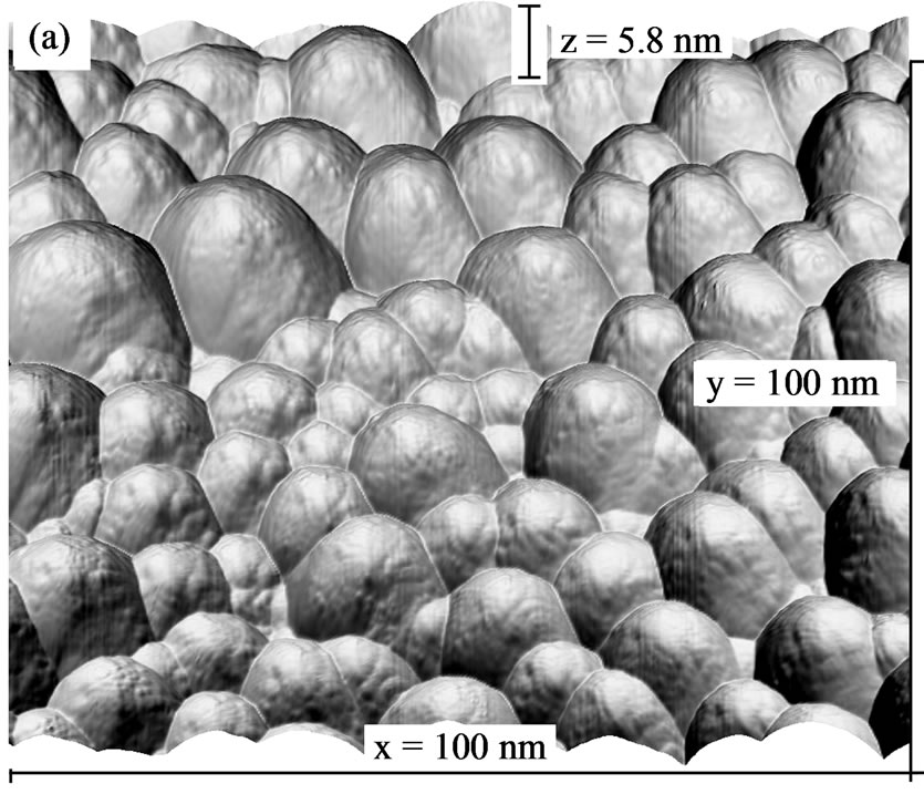

Figure 3. STM images of the oxidized Si(111) surface (a) before and after Ge deposition at the amount of (b) 1, (c) 2 and (d) 3 BL at 590˚C. The images have the same lateral scale.
smaller height. The continuous action of reaction (1) results in complete decomposition of the SiO2 film.
4. Ge growth at High Temperatures
After Ge island formation at the initial growth stage, the further Ge deposition or the sample annealing lead to the formation of large islands, when the temperature is in the range from 590˚C to 650˚C (Figure 4). The flat areas between the islands exhibit the 5 × 5 reconstruction which is normally observed for the 2 BL Ge wetting layers grown on the bare Si(111) substrates [29-31]. The (111) planes on top of the islands possess the 7 × 7 reconstruction that is similar for that known for Ge islands grown on the bare Si(111) surfaces [32-34]. The traces of the presence of threading dislocations in the islands were not found. The driving force for such surface morphology transformation is the lattice strain.
The Ge growth on the bare Si(111) surfaces has been studied in details [6-18,29-33]. For comparison with the above results the STM data for the Ge growth on the bare Si(111) surfaces at temperatures of 530˚C are shown in Figure 5. Deposited Ge forms large flat islands which are surrounded by trenches several nanometers deep [Figure 5(a)] [17,18]. The top plane of the islands has the 7 × 7 reconstruction [Figure 5(b)] [32,33]. The reconstructed surface is slightly undulating and that reflects the presence of the dislocation network lying in Ge near the Ge/Si interface. The Ge islands also contain the
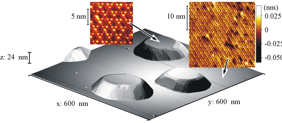
Figure 4. STM data for Ge islands obtained after 12 BL Ge deposition on the oxidized Si(111) surfaces at 630˚C. Insets show STM images of an 11 nm2 area on the island top plane with the 7 × 7 reconstruction and of a 26 nm2 area between the islands with the 5 × 5 reconstruction. The images were obtained at the bias voltages of −2.4 and 2.4 V, respectively, and the current of 20 pA.
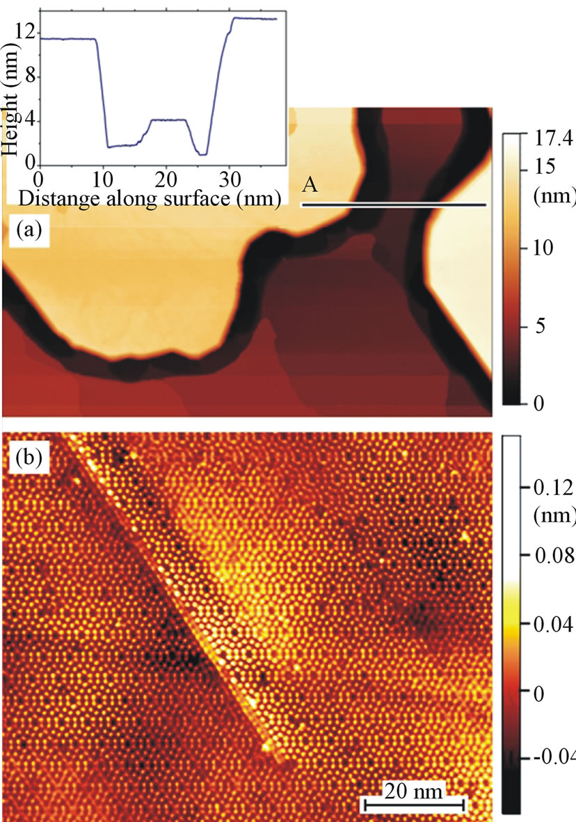
Figure 5. STM images obtained after 10 BL Ge deposition on the bare Si(111) surface at 530˚C. (a) Area with the fragments of two flat Ge islands surrounded by trenches. (b) Surface structure of a Ge island obtained at a bias voltage of −2.4 eV. Inset represents the height profile along the line marked by A in (a).
threading dislocations, as shown in Figure 5(b) [11-13]. When the islands start to coalesce at the further Ge deposition, the presence of the deep trenches around the islands gives rise to the formation of deep pits in the Ge layer. The important thing is that the dislocations appear in the Ge layer even if the surfactants are used to obtain continuous Ge layers on Si(111).
The surface morphology of Ge layers grown on bare and oxidized Si(111) surfaces at high temperatures is essentially different. The Ge growth on the bare Si(111) surfaces is accompanied by a significant intermixing of Ge and Si atoms that occurs to reduce the lattice strain [17,18,34]. During the Ge wetting layer formation, events of the intermixing happen preferably at the moment of embedding of deposited Ge atoms into the surface. After the appearance of three-dimensional islands, the strongest lattice strain appears along the perimeter of the islands [17,18]. This leads to the formation of trenches around the islands. The absence of the trenches, thus, suggests that the Ge islands are less strained when the oxidized Si(111) surface.
Dark and bright spots in the STM images of the 5 × 5 reconstructed surface obtained from the areas between the islands (inset in Figure 4) shows the presence of structural defects, which are probably traces of the SiO2 film. The residues of the SiO2 film can reduce the strain between the Ge wetting layer and the Si substrate. If so, there would be no sufficiently strong driving forces also for Ge-Si intermixing during the formation the Ge wetting layer.
The Ge deposition on the oxidized Si(111) surface at the temperature of 650˚C and higher results in the appearance of relatively large and small islands. The large islands are surrounded by rather deep trenches and have a high aspect ratio of 0.2 (Figure 6) whose value may reflect the content of Si in the Ge islands [35]. Such characteristics of the surface morphology indicate the appearance of a significant strain between the islands and the substrate due to the reduction of residuals of the SiO2 film at the Ge/Si interface.
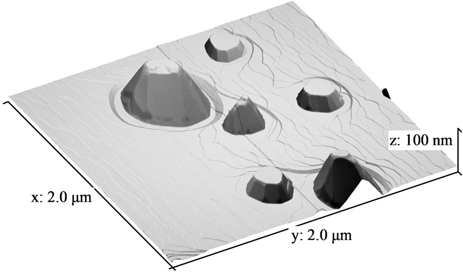
Figure 6. STM image obtained after 4 nm Ge deposition on the oxidized Si(111) surface at 650˚C.
5. Shape of Ge Islands Grown at High Temperatures
Figure 7 shows the data that were used to identify the facets orientation at the islands sidewalls appeared after Ge deposition on the oxidized Si(111) surfaces at temperatures in the range of 570˚C - 640˚C, at which trenches around the islands do not form. The data show that the sidewalls are mainly faceted by {311} planes and groups of facets with orientations close to {110} planes. Other facets occupy a much smaller part of the sidewalls and serve to smoothly join these main facets between themselves and also with the (111) plane on the flat top of the islands. The {311} facets are known to be the major stable planes for unstrained Ge and Si islands [36-40].
Among the facets with orientations near {110}, the largest areas on the sidewalls occupy planes inclined from (111) by angle θ of 27˚ - 29˚ and having angular divergence Δφ = 20.5˚ - 22.5˚ in the map of stereographic projections shown in Figure 7. The observation of
 (a)
(a)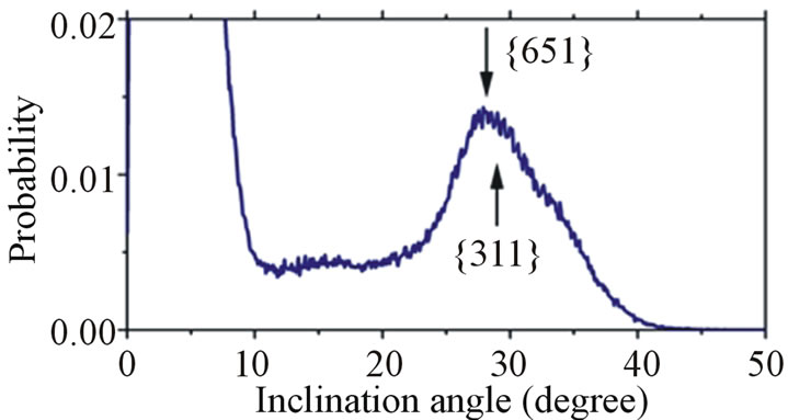 (b)
(b)
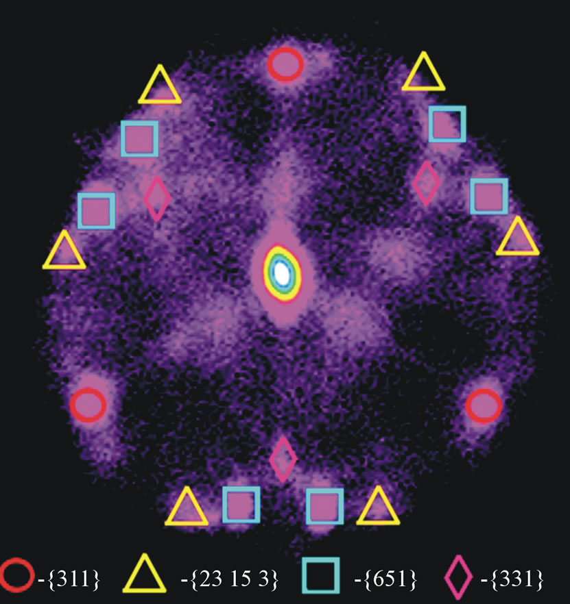
Figure 7. (a) The map of stereographic projections for surface areas and (b) portion of the areas as a function of their inclination angle with respect to the sample surface obtained from the STM image presented in Figure 4. The brightness in (a) is proportional to the size of the corresponding areas on the surface.
stable Ge facets with such an orientation has not been reported on. For Si surfaces the facets that have close orientations are {23 4 20} (θ = 30˚ and Δφ = 16.9˚), which were classified as MAJOR, and {651} (θ = 28.4˚ and Δφ = 21.5˚) (MINOR) [41]. The last facets have the orientations that are in good agreement with our experimental data and they are characterized by bright spots in the map of stereographic projections, covering relatively large sidewalls areas of the Ge islands.
Other facets with the orientations around {110} are identified to be {331} and {23 15 3}. These facets were previously classified as MAJOR for Ge [37]. However, they produce low-intense spots in the map shown in Figure 7(a).
The surface morphology of Ge layers grown at relatively high temperatures on the oxidized Si(111) surfaces composed of Ge wetting layer areas and islands which shape is determined by energetically preferable facets. This is essentially different from that observed for the bare Si(111) surfaces, where the surface morphology contains flat islands without well defined facets on the sidewalls, deep trenches around the islands, threading dislocations and traces of the presence of the dislocation network near the Ge-Si interface (Figure 5). The difference arises from the difference in the lattice strain.
6. Influence of the Initial Growth Stage on Subsequent Ge Growth
The above results suggest that, in order to prevent the formation of large islands, the growth of Ge layers on the oxidized Si(111) surfaces should be carried out within several stages that differ in temperature. The initial stage at a high temperature in the range of 570˚C - 650˚C serves for the formation of nanoareas of bare Si surfaces and then that of epitaxial Ge nanoisland arrays with the concentration of the order of 1012 cm−2. The temperature of the next growth stage must be reduced to prevent the decomposition of SiO2 film residuals. The surface morphology obtained when the temperature was lowered to 430˚C is shown in Figure 8. The data in Figures 2 and 8 suggest that the preferable Ge coverage in the initial growth stage should be in the range of 1 - 2 BL. A larger coverage leads to a considerable variation of the islands in size and to non-uniformity in their spatial distribution due to the partial islands coalescence (Figure 2(d))
7. Surface Morphology of Ge Layers Grown within Two Stages
As the Ge coverage increases to 30 BL in the two-stage growth, the facets appear on the sidewalls of the islands and the top of the islands becomes flat with (111) orientation. The data in Figure 9 show that the largest facets on the sidewalls are {311}. They produce the brightest
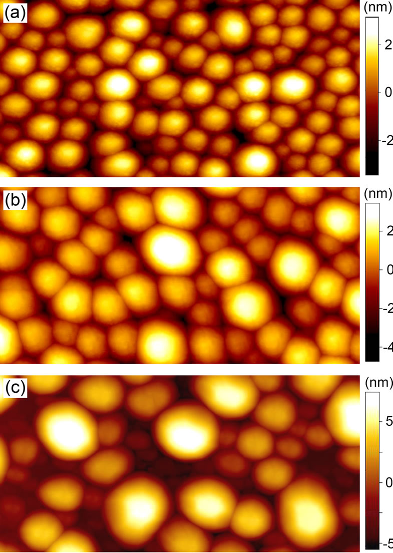
Figure 8. STM images of the oxidized Si(111) surface after Ge deposition at two stages. Ge was deposited for the coverage of (a) 1, (b) 2 and (d) 3 BL at 610˚C at the initial stage and then at 430˚C for the total coverage of 10 BL. The size of surface areas in the images is 100 × 50 nm.
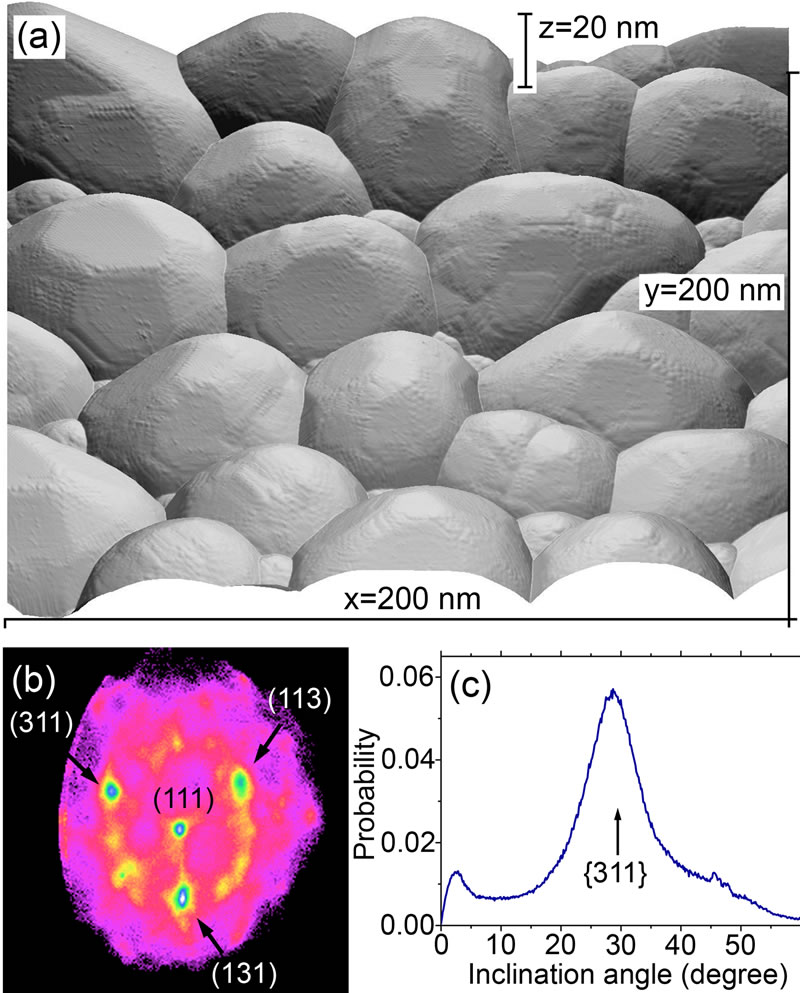
Figure 9. (a) STM image of the oxidized Si(111) surface after Ge deposition in two stages. Ge was deposited for a coverage of 2 BL at 610˚C and then at 500˚C for 30 BL. (b) The map of stereographic projections of surface areas and (c) portion of the areas as a function of their inclination angle from the sample surface obtained from the STM image.
spots in the map of stereographic projections (Figure 9(b)). The sidewalls also contain small-sized facets with orientations around {110}. The large peak in Figure 9(c) shows that the facets on the sidewalls preferably incline from (111) by the angles of 28˚ - 30˚.
The coalescence of islands under further Ge deposition leads to a significant increase of the flat (111) areas (Figure 10). They undergo c(2 × 4) and c(2 × 8) reconstructions which are typical of the (111) surfaces of bulk Ge [42-44]. The observation of the reconstructions thus indicates that the grown epitaxial Ge layers on Si(111) are unstrained.
The STM data show that the ratio of the top flat areas to the areas of other facets, inclined from (111), increases with decreasing the growth temperature from 550 to 360˚C. This occurs simultaneously with the decrease of the depth of depressions between the flat areas. This tendency does not extend to a low-temperature range. Figure 11 shows that the Ge layers grown at 250˚C - 300˚C indeed exhibit a relatively low surface roughness; however, the surface morphology is mainly composed of small-sized stepped facets such as {433}, {755} and {775}, whereas the flat (111) areas occupy a relatively small portion of the surface. The root-mean-square roughness was estimated from the STM image, shown in Figure 11, to be about 2.8 nm for the 140 nm thick Ge
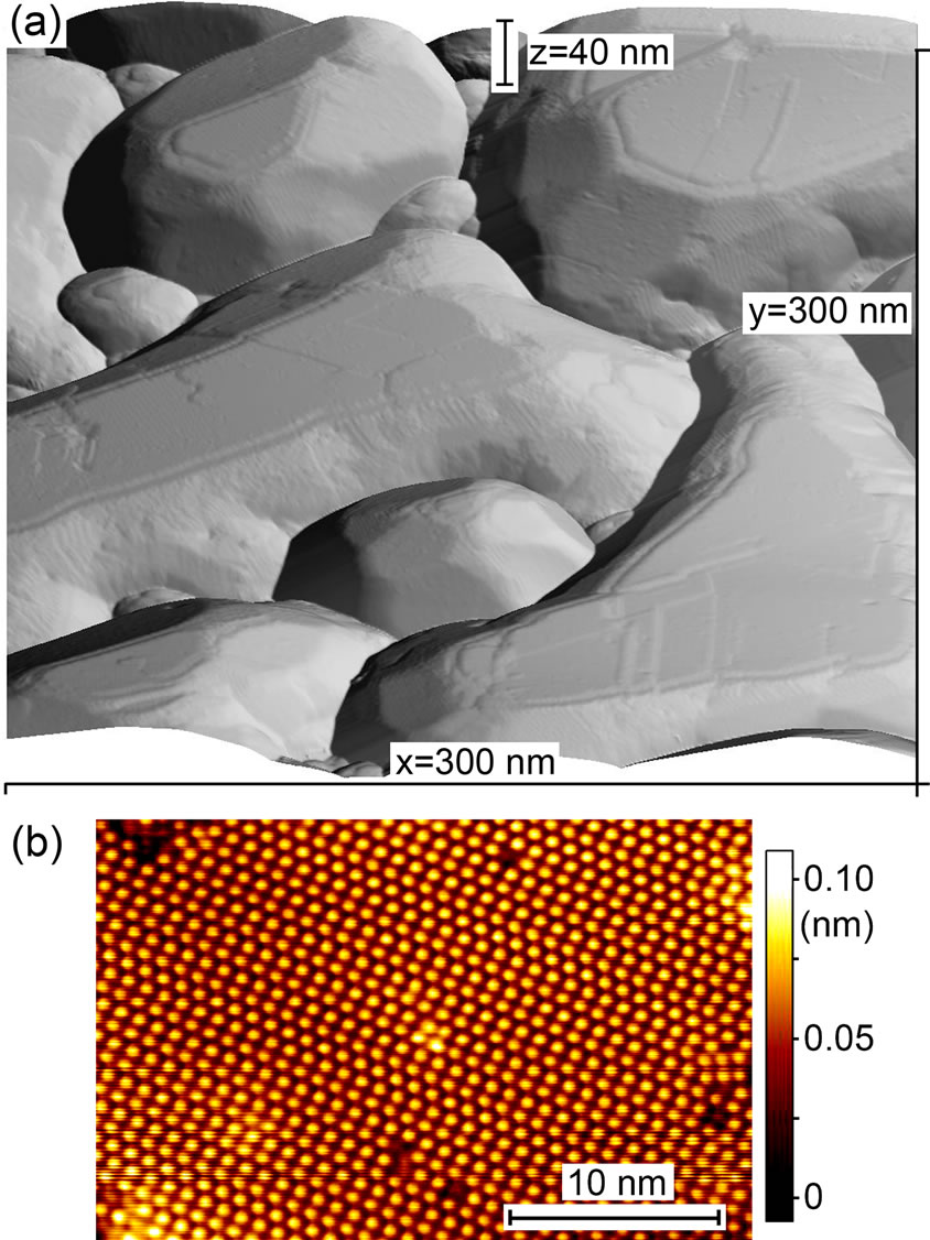
Figure 10. (a) STM image of the oxidized Si(111) surface after Ge deposition in two stages. Ge was deposited for a coverage of 1 BL at 620˚C and then at 360˚C for 85 BL. (b) STM image of the c(2 × 4) and c(2 × 8) reconstructions observed on flat areas of the Ge layer.
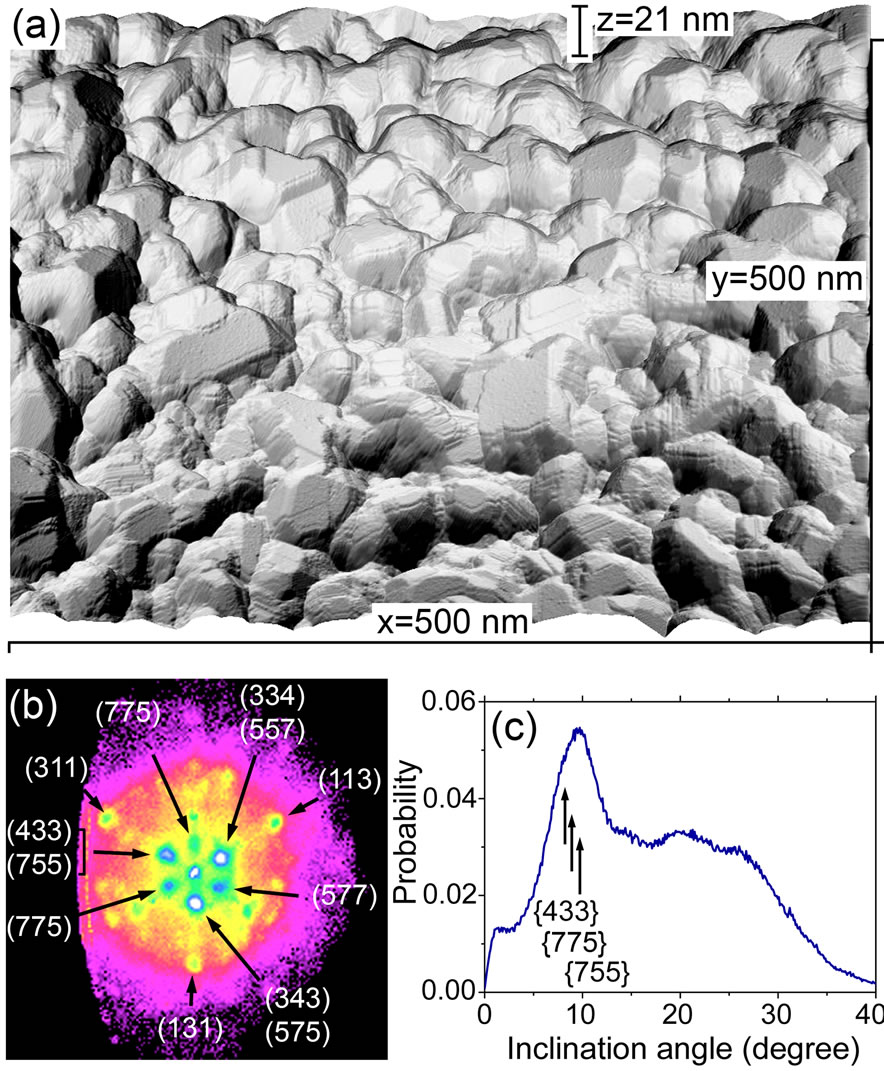
Figure 11. (a) STM image of the oxidized Si(111) surface after Ge deposition at two stages. Ge was deposited for the coverage of 2 BL at 590˚C and then at temperatures in the range between 250 and 300˚C for the total coverage of 140 nm. (b) The map of stereographic projections of surface areas and (c) portion of the areas as a function of their inclination angle from the sample surface obtained from the STM image.
layer. The most prevalent {433} and {755} facets consist of atomic steps with edges towards , which are the sort of stepped surfaces that were observed on the Ge surfaces cleaved in vacuum [45] and found to be stable on the vicinal Ge surfaces inclined from (111) [46].
8. Discussion
The idea of nanocontact epitaxy is to create the conditions for reducing a strain between the growing layer and the substrate by decreasing the area of their direct contact [20,21]. The Ge deposition of the oxidized Si surface produces bare Si areas in the SiO2 film, which are a few nanometers in size and separated by the distance of 7 - 10 nm [22,47]. Transmission electron microscopy data reveal shifts of the Ge lattice with respect to the Si lattice at the Si/Ge interface that occurs in places where Ge is separated from Si by the residuals of the SiO2 film [20]. In order to compensate the 4.2% lattice mismatch between Ge and Si, the shift should occur at the period of ~26 atoms, i.e., over the distance of 10 nm for the interface with (111) orientation. This distance is close to the average separation between the areas of bare Si that appear under Ge deposition on the oxidized Si(111) surfaces in the high-temperature range [22,23]. As shown here, the Ge layers with a significantly reduced stain can be epitaxially grown on Si(111) using this technique.
After the formation of epitaxial Ge nanoislands, the further Ge deposition at low temperatures leads to the growth and coalescence of the islands. In the places of the coalescence the stacking faults appear. Their concentration essentially depends on the growth temperature. The higher temperature provides the formation of higher crystalline quality Ge layers. At the same time, the temperature influences the surface morphology of the growing Ge layer. At relatively high temperatures, the surface morphology is composed of well-defined facets of energetically favorable planes; this does not, however, lead to a flat surface with the (111) orientation. The roughness of the surface can be decreased by decreasing the growth temperature. Thus, the temperature acts in different ways: i.e., the use of high temperatures improves the crystalline quality of Ge layers, but it induces the formation of a rather large roughness, whereas the use of low temperatures flattens the surface, but introduces crystal defects. This feature is an obstacle in obtaining atomically flat, about 100 nm thick, Ge layers with a high crystalline quality on Si(111) substrates.
The Ge layers grown on bare and oxidized Si(111) surfaces are characterized by the substantially different surface morphology caused by a difference in the lattice strain. The strong Si-Ge intermixing under the strain leads to the formation of deep trenches in Si substrates around large flat Ge islands [17,18] and the network of threading dislocations [11-3]. Even the use of surfactants does not allow one avoiding the dislocation formation. In case of oxidized Si surfaces, the role of strain is significantly reduced. As a result, the surface morphology has no sharp corners and steep facets on the sidewalls. Instead, it includes some additional faceting planes, such as {775}, {755} and {761}, which are not observed for Ge layers grown on the bare Si surfaces.
The use of the oxidized Si surface solves the problem of the strong Ge/Si lattice stain and significantly reduces the Ge-Si intermixing, but it does not provide obtaining thin Ge layers with atomically flat surfaces. It is suggested that the smoothing of the surface of growing layers can be achieved with the help of surfactants, as it has been experimentally and theoretically shown [48-50]. Surfactants also facilitate the surface diffusion of deposited atoms thereby providing the improvement of the crystalline quality of layers growing at low temperatures.
9. Conclusion
The initial Ge deposition on the oxidized Si(111) surfaces at temperatures in the range of 570˚C - 650˚C results in the formation of nanoareas of bare Si and Ge nanoislands arrays. Further Ge deposition leads to the decomposition of the SiO2 film residuals and to the formation of the Ge wetting layer and large islands. A comparison of Ge deposition on bare and oxidized Si(111) surfaces shows that the Ge/Si lattice stain is substantially reduced in the latter case. To obtain nanoareas of bare Si and homogeneous arrays of epitaxial Ge nanoislands, the preferable Ge coverage in the initial stage is found to be 1 - 2 BL. The temperature must then be decreased to 500˚C or less to stop the SiO2 film decomposition. After lowering the temperature, the shape of the growing islands evolves from rounded to faceted with a flat (111) plane on top. At the coverage of 30 - 140 nm, in addition to the (111) flat areas, the surface morphology is composed of {311} facets and facets lying around {110} and (111). The flat (111) areas exhibit the c(2 × 8) reconstruction that is typical of unstrained bulk Ge. The use of oxidized Si(111) surfaces allows one to obtain thin continuous epitaxial Ge layers on Si(111); however, the suppression of three-dimensional growth is still required to make the layers atomically flat.
10. Acknowledgements
We are grateful for the financial support by the Russian Foundation for Basic Research (Grant 11-07-00475-а), the Program of the Presidium of the Russian Academy of Sciences (project 24.21), and the Ministry of Education and Science of the Russian Federation (contract No. 16.518.11.7091).
REFERENCES
- K. Volz, A. Beyer, W. Witte, J. Ohlmann, I. Németh, B. Kunert and W. Stolz, “GaP-Nucleation on Exact Si(001) Substrates for III/V Device Integration,” Journal of Crystal Growth, Vol. 315, No. 1, 2011, pp. 37-47. doi:10.1016/j.jcrysgro.2010.10.036
- S. G. Ghalamestani, M. Berg, K. A. Dick and L.-E. Wernersson, “High Quality InAs and GaSb Thin Layers Grown on Si(111),” Journal of Crystal Growth, Vol. 332, No. 1, 2011, pp. 12-16. doi:10.1016/j.jcrysgro.2011.03.062
- Yu. B. Bolkhovityanov and O. P. Pchelyakov, “GaAs Epitaxy on Si Substrates: Modern Status of Research and Engineering,” Physics-Uspekhi, Vol. 51, No. 5, 2008, pp. 437-456. doi:10.1070/PU2008v051n05ABEH006529
- J. G. Cederberg, D. Leonhardt, J. J. Sheng, Q. Li, M. S. Carroll and S. M. Han, “GaAs/Si Epitaxial Integration Utilizing a Two-Step, Selectively Grown Ge Intermediate Layer,” Journal of Crystal Growth, Vol. 312, No. 8, 2010, pp. 1291-1296. doi:10.1016/j.jcrysgro.2009.10.061
- V. Destefanis, J.M. Hartmann, A. Abbadie, A. M. Papon and T. Billon, “Growth and Structural Properties of SiGe Virtual Substrates on Si(100), (110) and (111),” Journal of Crystal Growth, Vol. 311, No. 4, 2009, pp. 1070-1079. doi:10.1016/j.jcrysgro.2008.12.034
- P. M. J. Maré, K. Nakagawa, F. M. Mulders, J. F. Van der Veen and K. L. Kavanagh, “Thin Epitaxial Ge-Si(111) Films: Study and Control of Morphology,” Surface Science, Vol. 191, No. 3, 1987, pp. 305-328. doi:10.1016/S0039-6028(87)81180-9
- U. Köhler, O. Jusko, G. Pietsch, B. Müller and M. Henzler, “Strained-Layer Growth and Islanding of Germanium on Si (111)-(7 × 7) Studied with STM,” Surface Science, Vol. 248, No. 3, 1991, pp. 321-331. doi:10.1016/0039-6028(91)91178-Z
- A. A. Shklyaev, M. Shibata and M. Ichikawa, “Instability of Two-Dimensional Layers in the Stranski-Krastanov Growth Mode of Ge on Si(111),” Physical Review B, Vol. 58, No. 23, 1998, pp. 15647-15651. doi:10.1103/PhysRevB.58.15647
- B. Voigtländer and A. Zinner, “Simultaneous Molecular Beam Epitaxy Growth and Scanning Tunneling Microscopy Imaging during Ge/Si Epitaxy,” Applied Physics Letters, Vol. 63, No. 2, 1993, pp. 3055-3057. doi:10.1063/1.110256
- A. A. Shklyaev, M. Shibata and M. Ichikawa, “Ge Islands on Si(111) at Coverages near the Transition from TwoDimensional to Three-Dimensional Growth,” Surface Science, Vol. 416, No. 1, 1998, pp. 192-199. doi:10.1016/S0039-6028(98)00580-9
- S. Y. Shiryaev, F. Jensen, J. L. Hansen, J. W. Petersen and A. N. Larsen, “Nanoscale Structuring by Misfit Dislocations in Si1-xGex/Si Epitaxial Systems,” Physical Review Letters, Vol. 78, No. 3, 1997, pp. 503-506. doi:10.1103/PhysRevLett.78.503
- B. Voigtländer and N. Theuerkauf, “Ordered Growth of Ge Islands above a Misfit Dislocation Network in a Ge Layer on Si(111),” Surface Science, Vol. 461, No. 1-3, 2000, pp. L575-L580. doi:10.1016/S0039-6028(00)00620-8
- S. A. Teys, “Features of Atomic Processes at the Formation of a Wetting Layer and Nucleation of Three-Dimensional Ge Islands on Si(111) and Si(100) Surfaces,” JETP Letters, Vol. 96, No. 12, 2013, pp. 794-802. doi:10.1134/S0021364012240113
- R. Gunnella, P. Castrucci, N. Pinto, I. Diavoli, D. Sébilleau and M. De Crescenzi, “X-Ray Photoelectron-Diffraction Study of Intermixing and Morphology at the Ge/ Si(001) and Ge/Sb/Si(001) Interface,” Physical Review B, Vol. 54, No. 12, 1996, pp. 8882-8891. doi:10.1103/PhysRevB.54.8882
- X. R. Qin, B. S. Swartzentruber and M. G. Lagally, “Scanning Tunneling Microscopy Identification of AtomicScale Intermixing on Si(100) at Submonolayer Ge Coverages,” Physical Review Letters, Vol. 85, No. 17, 2000, pp. 3660-3663. doi:10.1103/PhysRevLett.85.3660
- F. Ratto, F. Rosei, A. Locatelli, S. Cherifi, S. Fontana, S. Heun, P.-D. Szkutnik, A. Sgarlata, M. De Crescenzi and N. Motta, “Composition of Ge(Si) Islands in the Growth of Ge on Si(111) by x-Ray Spectromicroscopy,” Journal of Applied Physics, Vol. 97, No. 4, 2005, pp. 043516-1- 043516-8. doi:10.1063/1.1832747
- T. I. Kamins, E. C. Carr, R. S. Williams and S. J. Rosner, “Deposition of Three-Dimensional Ge Islands on Si(001) by Chemical Vapor Deposition at Atmospheric and Reduced Pressures,” Journal of Applied Physics, Vol. 81, No. 1, 1997, pp. 211-219. doi:10.1063/1.364084
- F. Boscherini, G. Capellini, L. Di Gaspare, M. De Seta, F. Rosei, A. Sgarlata, N. Motta and S. Mobilio, “Ge-Si Intermixing in Ge Quantum Dots on Si,” Thin Solid Films, Vol. 380, No. 1-2, 2000, pp. 173-175. doi:10.1016/S0040-6090(00)01496-6
- M. Valvo, C. Bongiorno, F. Giannazzo and A. Terrasi, “Localized Si Enrichment in Coherent Self-Assembled Ge Islands Grown by Molecular Beam Epitaxy on (001) Si Single Crystal,” Journal of Applied Physics, Vol. 113, No. 3, 2013, pp. 033513-1-033513-17. doi:10.1063/1.4775772
- Y. Nakamura, A. Murayama and M. Ichikawa, “Epitaxial Growth of High Quality Ge Films on Si(001) Substrates by Nanocontact Epitaxy,” Crystal Growth & Design, Vol. 11, No. 7, 2011, pp. 3301-3305. doi:10.1021/cg200609u
- Y. Nakamura, T. Miwa and M. Ichikawa, “Nanocontact Heteroepitaxy of thin GaSb and AlGaSb Films on Si Substrates Using Ultrahigh-Density Nanodot Seeds,” Nanotechnology, Vol. 22, No. 26, 2011, pp. 265301-1-265301- 7. doi:10.1088/0957-4484/22/26/265301
- A. A. Shklyaev, M. Shibata and M. Ichikawa, “HighDensity Ultrasmall Epitaxial Ge Islands on Si(111) Surfaces with a SiO2 Coverage,” Physical Review B, Vol. 62, No. 3, 2000, pp. 1540-1543. doi:10.1103/PhysRevB.62.1540
- A. A. Shklyaev and M. Ichikawa, “Extremely Dense Arrays of Germanium and Silicon Nanostructures,” PhysicsUspekhi, Vol. 51, No. 2, 2008, pp. 133-161. doi:10.1070/PU2008v051n02ABEH006344
- S. Ghosh, D. Leonhardt and S. M. Han, “Experimental and Theoretical Investigation of Thermal Stress Relief during Epitaxial Growth of Ge on Si Using Air-Gapped SiO2 Nanotemplates,” Applied Physics Letters, Vol. 99, No. 18, 2011, pp. 181911-1-181911-3. doi:10.1063/1.3659320
- V. Kuryliuk, O. Korotchenkov and A. Cantarero, “Carrier Confinement in Ge/Si Quantum Dots Grown with an Intermediate Ultrathin Oxide Layer,” Physical Review B, Vol. 85, No. 7, 2012, pp. 075406-1-075406-11. doi:10.1103/PhysRevB.85.075406
- N. Miyata, H. Watanabe and M. Ichikawa, “Thermal Decomposition of an Ultrathin Si Oxide Layer around a Si(001)-(2 × 1) Window,” Physical Review Letters, Vol. 84, No. 5, 2000, pp. 1043-1046. doi:10.1103/PhysRevLett.84.1043
- A. A. Shklyaev, M. Aono and T. Suzuki, “Influence of Growth Conditions on Subsequent Submonolayer Oxide Decomposition on Si(111),” Physical Review B, Vol. 54, No. 15, 1996, 10890-10895. doi:10.1103/PhysRevB.54.10890
- A. A. Shklyaev and S. M. Repinsky, “Investigation of Ge Surface Self-Diffusion by Determination of Changes in the Reflection Intensity Profiles of Low-Energy Electron Diffraction,” Soviet Physics Semiconductors, Vol. 14, No. 7, 1980, pp. 767-772.
- B. Voigtländer, “Fundamental Processes in Si/Si and Ge/ Si Epitaxy Studied by Scanning Tunneling Microscopy during Growth,” Surface Science Reports, Vol. 43, No. 5-8, 2001, pp. 127-254. doi:10.1016/S0167-5729(01)00012-7
- N. Motta, A. Sgarlata, R. Calarco, Q. Nguyen, J. Castro Cal, F. Patella, A. Balzarotti and M. De Crescenzi, “Growth of Ge-Si(111) Epitaxial Layers: Intermixing, Strain Relaxation and Island Formation,” Surface Science, Vol. 406, No. 1-3, 1998, pp. 254-263. doi:10.1016/S0039-6028(98)00121-6
- M. Stoffel, Y. Fagot-Révurat, A. Tejeda, B. Kierren, A. Nicolaou, P. Le Fèvre, F. Bertran, A. Taleb-Ibrahimi and D. Malterre, “Electron-phonon Coupling on Strained Ge/Si(111)-(5 × 5) Surfaces,” Physical Review B, Vol. 86, No. 19, 2012, pp. 195438-1-195438-7. doi:10.1103/PhysRevB.86.195438
- H. -J. Gossmann, J. C. Bean, L. C. Feldman, E. G. McRae and I. K. Robinson, “7 × 7 Reconstruction of Ge(111) Surfaces under Compressive Strain,” Physical Review Letters, Vol. 55, No. 10, 1985, pp. 1106-1109. doi:10.1103/PhysRevLett.55.1106
- U. Köhler, O. Jusko, G. Pietsch, B. Müller and M. Henzler, “Strained-Layer Growth and Islanding of Germanium on Si(111)-(7 × 7) Studied with STM,” Surface Science, Vol. 248, No. 3, 1991, pp. 321-331. doi:10.1016/0039-6028(91)91178-Z
- K. N. Romanyuk, A. A. Shklyaev, B. Z. Olshanetsky and A. V. Latyshev, “Formation of Ge Clusters at a Si(111)- Bi-√3 × √3 Surface,” JETP Letters, Vol. 93, No. 11, 2011, pp. 661-666. doi:10.1134/S0021364011110105
- G. Vastola, V. B. Shenoy, J. Guo and Y.-W. Zhang, “Coupled Evolution of Composition and Morphology in a Faceted Three-Dimensional Quantum Dot,” Physical Review B, Vol. 84, No. 3, 2011, pp. 035432-1-035432-7. doi:10.1103/PhysRevB.84.035432
- A. Laracuente, S. C. Erwin and L. J. Whitman, “Structure of Ge(113): Origin and Stability of Surface Self-Interstitials,” Physical Review Letters, Vol. 81, No. 23, 1998, pp. 5177-5180. doi:10.1103/PhysRevLett.81.5177
- Z. Gai, R. G. Zhao, X. Li and W. S. Yang, “Faceting and Nanoscale Faceting of Ge(hhl) Surfaces around (113),” Physical Review B, Vol. 58, No. 8, 1998, pp. 4572-4578. doi:10.1103/PhysRevB.58.4572
- A. A. Stekolnikov and F. Bechstedt, “Shape of Free and Constrained Group-IV Crystallites: Influence of Surface Energies,” Physical Review B, Vol. 72, No. 12, 2005, p. 125326. doi:10.1103/PhysRevB.72.125326
- J. T. Robinson, A. Rastelli, O. Schmidt and O. D. Dubon, “Global Faceting Behavior of Strained Ge Islands on Si,” Nanotechnology, Vol. 20, No. 8, 2009, Article ID: 085708. doi:10.1088/0957-4484/20/8/085708
- A. A. Shklyaev, K. N. Romanyuk, A. V. Latyshev and A. V. Arzhannikov, “Effect of Dislocations on the Shape of Islands during Silicon Growth on the Oxidized Si(111) Surface,” JETP Letters, Vol. 93, No. 6, 2011, pp. 442-445. doi:10.1134/S0021364011180147
- Z. Gai, R. G. Zhao, W. Li, Y. Fujikawa, T. Sakurai and W. S. Yang, “Major Stable Surface of Silicon: Si(20 4 23),” Physical Review B, Vol. 64, No. 12, 2001, Article ID: 125201. doi:10.1103/PhysRevB.64.125201
- M. Henzler, “Correlation between Surface Structure and Surface States at the Clean Germanium (111) Surface,” Journal of Applied Physics, Vol. 40, No. 9, 1969, pp. 3758-3765. doi:10.1063/1.1658268
- B. Z. Olshanetsky, S. M. Repinsky and A. A. Shklyaev, “LEED Investigation of Germanium Surfaces Cleaned by Sulphide Films, Structural Transitions on Clean Ge(110) Surfaces,” Surface Science, Vol. 64, No. 1, 1977, pp. 224- 236. doi:10.1016/0039-6028(77)90268-0
- M. Kuzmin, M. J. P. Punkkinen, P. Laukkanen, J. J. K. Lang, J. Dahl, V. Tuominen, M. Tuominen, R. E. Perälä, T. Balasubramanian, J. Adell, B. Johansson, L. Vitos, K. Kokko and I. J. Väyrynen, “Surface Core-Level Shifts on Ge (111)-c(2 × 8): Experiment and Theory,” Physical Review B, Vol. 83, No. 24, 2011, p. 245319. doi:10.1103/PhysRevB.83.245319
- M. Henzler, “The Roughness of Cleaved Semiconductor Surfaces,” Surface Science, Vol. 36, No. 1, 1973, pp. 109- 122. doi:10.1016/0039-6028(73)90249-5
- B. Z. Olshanetsky, S. M. Repinsky and A. A. Shklyaev, “LEED Studies of Vicinal Surfaces of Germanium,” Surface Science, Vol. 69, No. 1, 1977, pp. 205-217. doi:10.1016/0039-6028(77)90169-8
- A. A. Shklyaev and M. Ichikawa, “Effect of Interfaces on Quantum Confinement in Ge Dots Grown on Si Surfaces with a SiO2 Coverage,” Surface Science, Vol. 514, No. 1-3, 2002, pp. 19-26. doi:10.1016/S0039-6028(02)01602-3
- M. Copel, M. C. Reuter, M. Horn von Hoegen and R. M. Tromp, “Influence of Surfactants in Ge and Si Epitaxy on Si (001),” Physical Review B, Vol. 42, No. 18, 1990, pp. 11682-11689. doi:10.1103/PhysRevB.42.11682
- B. Voigtlander, A. Zinner, T. Weber and H. P. Bonzel, “Modification of Growth Kinetics in Surfactant-Mediated Epitaxy,” Physical Review B, Vol. 51, No. 12, 1995, pp. 7583-7591. doi:10.1103/PhysRevB.51.7583
- D. Kandel and E. Kaxiras, “Surfactant Mediated Crystal Growth of Semiconductors,” Physical Review Letters, Vol. 75, No. 14, 1995, pp. 2742-2745. doi:10.1103/PhysRevLett.75.2742