Open Access Library Journal
Vol.02 No.12(2015), Article ID:68898,10 pages
10.4236/oalib.1102108
Aluminum Doped ZnO Thin Films Using Chemical Spray Pyrolysis
Ramakrishnan Jayakrishnan
Department of Physics, Christian College, Kerala, India

Copyright © 2015 by author and OALib.
This work is licensed under the Creative Commons Attribution International License (CC BY).
http://creativecommons.org/licenses/by/4.0/


Received 12 November 2015; accepted 27 November 2015; published 2 December 2015
ABSTRACT
Aluminum doped ZnO thin films were grown using chemical spray pyrolysis. The doped films showed only blue and UV photoluminescence at room temperature. The position of the near band edge emission was found to agree with the theoretical value of ZnO nanocrystal band gap. The full width at half maximum for the near band edge emission at room temperature was found to be ~ 100 meV, which indicated films to be of very good device quality. The presence of a weak photoluminescence at 3.08 ± 0.02 eV in the films was assigned to defect related emission. We had shown in this report that it was possible to increase the efficiency of the photoluminescence by increasing the substrate temperature used for film growth. The optimized films showed resistivity of 1.5 × 10⁻² Ω∙cm.
Keywords:
Thin films, Chemical Spray Pyrolysis, ZnO, Photoluminescence, Excitons
Subject Areas: Analytical Chemistry

1. Introduction
The past decade has witnessed a significant improvement in the quality of zinc oxide (ZnO) single-crystal substrates and epitaxial films as result of revival and rapid expansion of research on ZnO as a semiconductor [1] - [5] . The high electron mobility, high thermal conductivity, wide and direct band gap and large exciton binding energy make ZnO ideal for a wide range of device applications like transparent thin-film transistors, photodetectors, light-emitting diodes and laser diodes that operate in the blue and ultraviolet region of the spectrum [6] - [12] . The free-exciton binding energy in ZnO is 60 meV [11] [12] . This large exciton binding energy indicates that efficient exciton emission in ZnO can persist at room temperature and higher [11] [12] . Since the oscillator strength of excitons is typically much larger than that of direct electron-hole transitions in direct gap semiconductors, the large exciton binding energy makes ZnO a promising material for optical devices that are based on exciton effects [13] . Due to a strong luminescence in the green-white region of the spectrum, ZnO is also a suitable material for phosphor applications. The emission spectrum has a peak at 495 nm and a very broad half-width of 0.4 eV [14] . The origin of the luminescence center and the luminescence mechanism are not really understood, being frequently attributed to oxygen vacancies or zinc interstitials, without any clear evidence [14] .
Most of the current technological applications of ZnO, such as varistors, transparent conductive electrodes for solar cells, piezoelectric devices and gas sensors, have made use of polycrystalline films that are grown by a variety of deposition techniques, mostly on glass substrates [15] . These techniques include chemical spray pyrolysis, screen painting, electrochemical deposition, sol-gel synthesis and oxidation of Zn films, which are characterized by requiring relatively low temperatures for film growth [5] [8] - [14] . However, for electronic and optoelectronic applications, high-quality single-crystal epitaxial films with minimal concentrations of native defects and controlled impurity incorporation are required [16] . For these, optimized growth and processing environments (partial pressures and temperature) are necessary. Current techniques that are recognized for this level of control include pulsed laser deposition (PLD), chemicalvapor deposition (CVD), metal-organic CVD (MOCVD) and molecular-beam epitaxy (MBE), and to a lesser extentsputtering [17] - [22] . Magnetron sputtering is recognized to be the most scalable technique, at the expense of lower crystalline quality, often resulting in columnar structures [15] .
We have been optimizing Chemical Spray Pyrolysis (CSP) technique for the growth of different binary and ternary semiconductor thin films for solar cell applications [23] [24] . The (002) plane in ZnO is considered to be the most ideal growth plane for opto-electronic device fabrication [25] . In the present work, we report on the effect of optimizing the substrate temperature, while maintaining the doping concentration and the spray rate to grow ZnO thin films with preferential orientation along the (002) plane using this technique. The optimized doping concentration is obtained through a detailed investigation reported earlier by us [5] . In the present work, we report on how we are able to improve the efficiency of near band edge (NBE) PL emission at room temperatureon optimally doped ZnO thin films. The full width at half maximum of the PL spectra gives characteristic information, which can be used to judge the sample quality [24] . Our results prove that CSP technique can be used to grow device quality ZnO films.
2. Experimental
ZnO thin films were prepared by spraying a solution containing a mixture of zinc acetate (99.9%) dissolved in distilled water, propanol and acetic acid in the ratio 50:47.5:2.5 on to glass substrates maintained at a suitable temperature. All chemicals used were from Sigma Aldrich of AR grade. In our previous report we had concluded that Al doped ZnO thin films can be grown using CSP technique with preferential orientation along (002) plane when the spray rate was maintained at 1 ml/min and the doping concentration was 1% [5] . There, however, the films were of poor crystalline quality. The spray rate of 1 ml/min was hence used for injecting the precursor solution onto the substrate for all trials reported in this report. Doping of ZnO films was carried out by mixing suitable quantity of Al (NO3)3∙9H2O (99.90%) solution to the spray precursor solution. Al (NO3)3∙9H2O solution was prepared in the same molarity as the spray precursor solution and 1% volumetric doping of the spray precursor solution was carried out for preparing all of the samples. Chemical Spray Pyrolysis was carried out using a unit developed in-house. The details of the experimental set up have been reported in detail by us [5] [24] . In each trail a sample was loaded with a mask so as to obtain a step profile. Then the thickness of the films was measuresd using a stylus surface profilometer (Dektak 6 M).
Structural analysis was done using X-ray diffraction (XRD) with a Rigaku (D.Max.C) X-ray diffractometer, having Cu Ka (l = 1.5405 Å) radiation and Ni filter operated at 30 kV and 20 mA. Optical absorption and transmission studies were carried out using UV-Vis-NIR spectrophotometer (Hitachi U-3410 Model). Photoluminescence studies were performed in an in-house assembled PL scanning system, by exciting the samples with 325 nm line of a He-Cd laser (Kimmon) and the emission spectrum was recorded using a USB2000 spectrophotometer. Details of the PL system were reported by us [26] - [28] . Electrical measurements were carried out using silver contacts separated by a distance of 1 cm. In this study, the sheet resistivity is calculated by the following equation:
 (1)
(1)
where r is the resistivity, Rs is the sheet resistance (Ω/sq) and d is the sample thickness.
3. Results and Discussion
Figure 1 shows the X-ray diffraction (XRD) spectra for samples prepared by varying the substrate temperature from 723 K to 873 K. The peaks of the XRD pattern correspond to those of the theoretical ZnO patterns from the JCPDS data file, with a hexagonal wurtzite structure of the bulk and lattice constants: a = 3.24982 Å, c = 5.20661 Å [20] . The analytical method was used to calculate the lattice constants (a = 3.00 Å, c = 5.20 Å) for the films [29] . The full width at half maximum (FWHM) of the (002) peak varied from 0.236˚ to 0.265˚ for the films. Another major orientation present is (101) with comparatively lower intensity. Therefore, we could conclude that the crystallites are highly oriented with their c-axes perpendicular to the plane of the substrate.
The volume of the spray solution was varied for each case so as to obtain thin films of the same thickness. The thickness of the samples was between 850 ± 100 nm. As the substrate temperature was increased it was observed that the films deposited exhibited improved growth along the (002) and (101) plane. It was observed that the preferential growth along the (002) plane for the films occurred in all cases as temperature was raised up to 848 K. Beyond this temperature the growth along this plane was not preferred. We assume that as the substrate temperature is increased lesser amount of oxygen is accommodated into the lattice which result in decrease in growth along the (002) plane. The grain size of the films from the XRD data was calculated using the Debye- Scherrer formula [29] :
 (2)
(2)
where “d” is the grain size, l = 1.5405 Å, β is the broadening of diffraction line measured at the half of its maximum intensity in radians and q is the angle of diffraction. Table 1 summarizes the effect of variation in substrate temperature on the grain size of the ZnO thin films. It is observed that films grown at 848 K have the smallest grain size.

Figure 1. XRD spectra for samples prepared by maintaining the substrate temperature at 723 K, 823 K, 848 K and 873 K.

Table 1. The variation in grain size, texture coefficient, thickness, theoretical band gap and band gap based on Tauc plot are tabulated with respect to the substrate temperature.
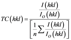
The texture coefficient (TC) represents the texture of a particular plane, whose deviation from unity implies the preferred growth. Quantitative information concerning the preferential crystallite orientation was obtained from another texture coefficient TC(hkl) defined as:
 (3)
(3)
where I(hkl) is the measured relative intensity of a plane (hkl) and I0(hkl) is the standard intensity of the plane (hkl) taken from the JCPDS data [30] . The value TC(hkl) = 1 represents films with randomly oriented crystallites, while higher values indicate the abundance of grains oriented in a given (hkl) direction. The variation of TC for the peaks of the wurzite lattice is presented in Table 1. It can be seen that the highest TC was in the (002) plane for ZnO thin film grown on substrate maintained at 848 K.
Figure 2 shows the transmission spectrum for the samples. Good surface quality and homogeneity of the films were confirmed from the appearance of interference fringes in the transmission spectra. Interference fringes occur when the film surface is highly reflecting, without much scattering/absorption in the bulk of the film. It is well established that in transparent metal oxides, metal to oxygen ratio decides the percentage of transmittance [31] . Optical constants were evaluated using the “envelope method” originally developed by Manifacier et al. [32] . If we assume that the film absorbs weakly and the substrate is completely transparent, then using the envelope method the refractive index (n) of the film on a transparent substrate can be evaluated from the transmission spectra. The refractive indices n at various wavelengths were calculated using the envelope curve for Tmax (TM) and Tmin (Tm) in the transmission spectra [32] . The expression for the refractive index is given by:
 (4)
(4)
where
 (5)
(5)
and ns is the refractive index of the substrate (ns = 1.52 for glass). Figure 3 shows the variation of the refractive index n in the range 300 - 2000 nm for the film prepared at 848 K. The thickness of the film was calculated using the equation:
 (6)
(6)
where n1 and n2 are the refractive indices corresponding to the wavelengths λ1 and λ2 respectively [32] . The thicknesses of the films are given in Table 1.
The PL of the ZnO thin films was measured at room temperature (Figure 4). There is an improvement in the radiative efficiency of the UV emission as substrate temperature is increased up to 848 K as evident in Figure 4. The high energy sides of the spectra are steep while the low energy side tail slowly. The emission spectra of all

Figure 2. Transmission spectra for samples prepared by maintaining the substrate temperature at 823 K, 848 K and 873 K.

Figure 3. Plot of simulated values of refractive index n versus wavelength.
samples have full width at half maximum ~100 meV at 300 K. The emission ranges from 3.27 to 2.96 eV for the samples indicating them to be unresolved UV emission. The emission for all samples could be fitted well with two peaks located at 3.20 ± 0.02 eV and 3.08 ± 0.02 eV. The emission at 3.20 ± 0.02 eV could be assigned to the near band edge emission (NBE). The FWHM of the NBE emission in our films are of the same order as that in ZnO nanocrystals and quantum dots grown using magnetron sputtering and MBE [33] - [35] . The mechanism of NBE emission at low temperature is well understood owing to the sharp and intense emission peaks [36] . Broadening of the NBE peak at higher temperature make it difficult to identify the emission mechanism. In majority of the published works, NBE emission has been attributed to free-exciton annihilation from the position of peak energy [37] [38] . When the exciton dissociates it creates a free electron and a free hole. Recombination of the electron-hole pair results in emission of photon with energy:

Figure 4. PL spectra for samples prepared by maintaining the substrate temperature at 723 K, 823 K, 848 K and 873 K.
 (7)
(7)
where Eg is the band gap and eex is the exciton binding energy. The band gap is calculated using Equation (7) and is shown in Table 2 along with the substrate temperature and the position of the NBE emission. A level at 3.06 eV below the conduction band was identified corresponding to the acceptor level VZn [38] . So we assume that the emission at 3.08 ± 0.02 eV might be due to the transition from the conduction band to the level due to VZn. Appearance of the emission at 3.08 ± 0.02 eV was observed only in optimally Al doped ZnO [5] . Hence the possibility of formation of a defect level due to zinc vacancy was more due to Al doping.
The emission by the nanocrystalline structure will have quantum size effect similar to that of quantum dots and can be described by the following equation [39] :
 (8)
(8)
The bulk band gap  is taken as 3.2 eV, and the bulk exciton binding energy
  can be taken as 60 meV [40] [41] . The electron and hole effective masses are taken as
  and
and , respect-
tively [42] . Additionally, h is Planck’s constant and R is the radius of ZnO nanocrystals. Figure 5 shows a plot of the nanocrystal band gap  versus the nanocrystal radius R. The solid curve is the theoretical fit of Equation (8), while the symbols are the grain sizes estimated from XRD result (Table 1) and their corresponding optical band gaps determined by applying the Tauc model [43] . The band gap does not show much variation with the crystallite size, which corresponds to various growth temperatures. This is mainly because the crystallite size is not small enough to show a distinct variation of the band gap. The inset in Figure 5 relates the NBE emission for the samples and the respective substrate temperature at which the films were grown. From Figure 5 and the inset, it can be seen that the position of the NBE emission in PL agrees with the theoretical curve. Hence we conclude that the PL measurement demonstrates that the emission comes from ZnO nanocrystals.
Table 2 shows the variation in resistivity of the samples prepared. Resistivity was observed to be the least for sample prepared at 848 K. The decrease in resistivity might be naturally due to the donor action of Aluminum. Since in all cases we used the same doping concentration we assume that on increasing substrate temperature, zinc might be progressively replaced by Al atom and since it belonged to group III, it could supply an additional electron contributing to the conductivity. Also Al could occupy interstitial position, again promoting conductivity. Generally it is expected that resistivity may increase due to the decrease in grain size and also due to the in-

Figure 5. Theoretical simulation on the effect of grain size on band gap for ZnO. Inset shows variation in position of the NBE emission with substrate temperature.
Table 2. The variation in resistivity of the samples, the position of the NBE emission and band gap calculated based on PL as a function of substrate temperature are tabulated.
crease in the grain boundary scattering. Since there was no appreciable decrease in grain size with Al doping the grain-boundary scattering effect might be less prominent in our results. We conclude that 848 K is the optimum temperature for 1% Al doping of ZnO when the spray rate is maintained at 1 ml/min.
4. Conclusion
In conclusion, we have demonstrated the improvement in efficiency of UV emitting, ZnO thin films using chemical spray pyrolysis technique. Defects are compensated to a high degree in Al doped ZnO thin films grown by this method. These doped films exhibit UV emission when excited with above band gap energy photons. It is possible to improve the radiative efficiency of the UV emission by optimizing substrate temperature. Energy of the near band edge emission agrees well with the theoretical band gap estimated for nanocrystals. Under optimized conditions, we can develop thin films with resistivity of 1.5 × 10⁻² Ωcm. The samples prepared at optimum condition show UV emission with FWHM of ~100 m eV at room temperature confirming their device quality comparable to films grown using MBE and sputtering. Based on our results we conclude that chemical spray pyrolysis is an economic and user friendly technique for the growth of device quality thin films.
Acknowledgements
The authors wish to thank Hind High Vacuum India Private Limited for the financial assistance in carrying out this work.
Cite this paper
Ramakrishnan Jayakrishnan, (2015) Aluminum Doped ZnO Thin Films Using Chemical Spray Pyrolysis. Open Access Library Journal,02,1-10. doi: 10.4236/oalib.1102108
References
- 1. Evans, S.M., Giles, N.C., Halliburton, L.E. and Kappers, L.A. (2008) Further Characterization of Oxygen Vacancies and Zinc Vacancies in Electron-Irradiated ZnO. Journal of Applied Physics, 103, Article ID: 043710.
http://dx.doi.org/10.1063/1.2833432 - 2. Tainoff, D., Masenelli, B., Mélinon, P., Belsky, A., Ledoux, G., Amans, D., Dujardin, C., Fedorov, N. and Martin, P. (2010) Competition between Exciton-Phonon Interaction and Defects States in the 3.31 eV Band in ZnO. Physical Review B, 81, Article ID: 115304.
http://dx.doi.org/10.1103/PhysRevB.81.115304 - 3. Johnston, K., Henry, M.O., McCabe, D., McGlynn, E., Dietrich, M., Alves, E. and Xia, M. (2006) Identification of Donor-Related Impurities in ZnO Using Photoluminescence and Radiotracer Techniques. Physical Review B, 73, Article ID: 165212.
http://dx.doi.org/10.1103/PhysRevB.73.165212 - 4. Janotti, A. and Van de Walle, C.G. (2007) Native Point Defects in ZnO. Physical Review B, 76, Article ID: 165202.
http://dx.doi.org/10.1103/PhysRevB.76.165202 - 5. Mohanachandran, R.J., Sreekumar, R., Sudha Kartha, C. and Vijayakumar, K.P. (2012) ZnO Thin Films with Blue Emission Grown Using Chemical Spray Pyrolysis. Materials Science in Semiconductor Processing, 16, 326-331.
http://dx.doi.org/10.1016/j.mssp.2012.10.003 - 6. Chopra, K.L., Major, S. and Pandya, D.K. (1983) Transparent conductors—A Status Review. Thin Solid Films, 102, 1.
- 7. Pages, H.R., Lmoc, J.R., Pinho and Losch, W. (1989) Properties of Al Doped ZnO Films Produced by Spray Pyrolysis. Proceedings of 9th Photovoltaic Solar Energy Conference, Frieburg, 25-29 September 1989, 63.
- 8. Hagiwara, V., Nakada, T. and Kunioka, A. (2001) Improved Jsc in CIGS Thin Film Solar Cells Using a Transparent Conducting ZnO: B Window Layer. Solar Energy Materials and Solar Cells, 67, 267-271.
http://dx.doi.org/10.1016/S0927-0248(00)00291-9 - 9. Reghu, N. and Kutty, T.R.N. (1992) Relationship between Nonlinear Resistivity and the Varistor Forming Mechanism in ZnO Ceramics Applied Physics Letters, 60, 100.
http://dx.doi.org/10.1063/1.107360 - 10. Dela, M., Olvera, L., Maldonado, A., Asomoza, R., Konagai, M. and Asomoza, M. (1993) Characteristics of ZnO: Ga Thin Films Prepared by Chemical Spray Using Two Different Zn and Ga Precursors. Thin Solid Films, 229, 196.
- 11. Shih, W.-C. and Wu, M.-S. (1994) Growth of ZnO Films on GaAs Substrates with a SiO2 Buffer Layer by RF Planar Magnetron Sputtering for Surface Acoustic Wave Applications. Journal of Crystal Growth, 137, 319-325.
http://dx.doi.org/10.1016/0022-0248(94)90968-7 - 12. Cordaro, J.F., Shim, Y. and May, J.E. (1986) Bulk Electron Traps in Zinc Oxide Varistors. Journal of Applied Physics, 60, 4186.
http://dx.doi.org/10.1063/1.337504 - 13. Sang, B., Yamada, A. and Konagai, M. (1998) Textured ZnO Thin Films for Solar Cells Grown by a Two-Step Process with the Atomic Layer Deposition Technique. Japanese Journal of Applied Physics, 37, L206.
http://dx.doi.org/10.1143/JJAP.37.L206 - 14. Shionoya, S. and Yen, W.H. (Eds.) (1997) Phosphor Handbook by Phosphor Research Society. CRC Press, Boca Raton.
- 15. Janotti, A. and Van de Walle, C.G. (2009) Fundamentals of Zinc Oxide as a Semiconductor. Reports on Progress in Physics, 72, Article ID: 126501.
http://dx.doi.org/10.1088/0034-4885/72/12/126501 - 16. Van de Walle, C.G. (2000) Hydrogen as a Cause of Doping in Zinc Oxide. Physical Review Letters, 85, 1012-1015.
http://dx.doi.org/10.1103/PhysRevLett.85.1012 - 17. Krc, J., Zeman, M., Kluth, O., Smole, F. and Topic, M. (2003) Effect of Surface Roughness of ZnO:Al Films on Light Scattering in Hydrogenated Amorphous Silicon Solar Cells. Thin Solid Films, 426, 296-304.
http://dx.doi.org/10.1016/S0040-6090(03)00006-3 - 18. Water, W. and Chu, S.-Y. (2002) Physical and Structural Properties of ZnO Sputtered Films. Materials Letters, 55, 67-72.
http://dx.doi.org/10.1016/S0167-577X(01)00621-8 - 19. Aly, S.A., Elsayed, N.Z. and Kaid, M.A. (2001) Effect of Annealing on the Optical Properties of Thermally Evaporated ZnO Films. Vacuum, 61, 1-7.
http://dx.doi.org/10.1016/S0042-207X(00)00415-2 - 20. Lee, J.-H., Ko, K.-H. and Park, B.-O. (2003) Electrical and Optical Properties of ZnO Transparent Conducting Films by the Sol-Gel Method. Journal of Crystal Growth, 247, 119-125.
http://dx.doi.org/10.1016/S0022-0248(02)01907-3 - 21. Myoung, J.-M., Yoon, W.-H., Lee, D.-H., Yun, I., Bae, S.-H. and Lee, S.-Y. (2002) Effects of Thickness Variation on Properties of ZnO Thin Films Grown by Pulsed Laser Deposition. Japanese Journal of Applied Physics, 41, 28-31.
http://dx.doi.org/10.1143/JJAP.41.28 - 22. Ko, H.-J., Yao, T., Chen, Y. and Hong, S.-K. (2002) Investigation of ZnO Epilayers Grown under Various Zn/O Ratios by Plasma-Assisted Molecular-Beam Epitaxy. Journal of Applied Physics, 92, 4354.
http://dx.doi.org/10.1063/1.1509103 - 23. John, T.T., Mathew, M., Sudha Kartha, C., Vijayakumar, K.P., Abe, T. and Kashiwaba, Y. (2005) CuInS2/In2S3 Thin Film Solar Cell Using Spray Pyrolysis Technique Having 9.5% Efficiency. Solar Energy Materials & Solar Cells, 89, 27-36.
http://dx.doi.org/10.1016/j.solmat.2004.12.005 - 24. Sebastian, T., Jayakrishnan, R., SudhaKartha, C. and Vijayakumar, K.P. (2009) Characterization of Spray Pyrolysed CuInS2 Thin Films. The Open Surface Science Journal, 1, 1-6.
http://dx.doi.org/10.2174/1876531900901010001 - 25. Choopun, S., Vispute, R.D., Noch, W., Balsamo, A., Sharma, R.P., Venkatesan, T., Lliadis, A. and Look, D.C. (1999) Oxygen Pressure-Tuned Epitaxy and Optoelectronic Properties of Laser-Deposited ZnO Films on Sapphire. Applied Physics Letters, 75, 3947.
http://dx.doi.org/10.1063/1.125503 - 26. Jayakrishnan, R., Sebastian, T., Sudha Kartha, C. and Vijayakumar, K.P. (2006) Room Temperature Photoluminescence Surface Mapping. Journal of Physics: Conference Series, 28, 62-65.
http://dx.doi.org/10.1088/1742-6596/28/1/012 - 27. Jayakrishnan, R., Ratheesh Kumar, P.M., Sudha Kartha, C. and Vijayakumar, K.P. (2006) Surface Topology Using Laser Backscattering and Photoluminescence on Cu- and In-Rich CuInSe2 Thin Films. Measurement Science and Technology, 17, 3301-3308.
http://dx.doi.org/10.1088/0957-0233/17/12/016 - 28. Jayakrishnan, R., Sebastian, T., John, T.T., Sudha Kartha, C. and Vijayakumar, K.P. (2007) Photoconductivity in Sprayed β-In2S3 Thin Films under Sub-Band-Gap Excitation of 1.96 eV. Journal of Applied Physics, 102, Article ID: 043109.
http://dx.doi.org/10.1063/1.2770830 - 29. Cullity, B.D. and Stock, S.R. (2001) Elements of X-Ray Diffraction. 3rd Edition, Prentice Hall, New York.
- 30. Romero, R., Leinen, D., Dalchiele, E.A., Ramos-Barrado, J.R. and Martin, F. (2006) The Effects of Zinc Acetate and Zinc Chloride Precursors on the Preferred Crystalline Orientation of ZnO and Aldoped ZnO Thin Films Obtained by Spray Pyrolysis. Thin Solid Films, 515, 1942-1949.
http://dx.doi.org/10.1016/j.tsf.2006.07.152 - 31. Ratheesh Kumar, P.M., Sudha Kartha, C., Vijayakumar, K.P., Singh, F., Avasthi, D.K., Abe, T., Kashiwaba, Y., Okram, G.S., Kumar, M. and Kumar, S. (2005) Modifications of ZnO Thin Films under Dense Electronic Excitation. Journal of Applied Physics, 97, Article ID: 013509.
- 32. Manifacier, J.C., Gasiot, J. and Fillard, J.P. (1976) A Simple Method for the Determination of the Optical Constants n, h and the Thickness of a Weakly Absorbing Thin Film. Journal of Physics E: Scientific Instruments, 9, 1002-1004.
- 33. Zhao, K. and Shen, A. (2012) Increasing ZnO Growth Rate by Modifying Oxygen Plasma Conditions in Plasma-Assisted Molecular Beam Epitaxy. World Journal of Condensed Matter Physics, 2, 160-164.
http://dx.doi.org/10.4236/wjcmp.2012.23026 - 34. Xiu, F., Yanga, Z., Zhao, D., Liu, J., Alim, K.A., Balandin, A.A., Itkis, M.E. and Haddon, R.C. (2006) ZnO Growth on Si with Low-Temperature ZnO Buffer Layers by ECR-Assisted MBE. Journal of Crystal Growth, 286, 61-65.
http://dx.doi.org/10.1016/j.jcrysgro.2005.09.056 - 35. Fonoberov, V.A., Alim, K.A., Balandin, A.A., Xiu, F. and Liu, J. (2006) Photoluminescence Investigation of the Carrier Recombination Processes in ZnO Quantum Dots and Nanocrystals. Physical Review B, 73, Article ID: 165317.
http://dx.doi.org/10.1103/PhysRevB.73.165317 - 36. Klingshirn, C. (1975) The Luminescence of ZnO under High One- and Two-Quantum Excitation. Physica Status Solidi B, 71, 547-556.
http://dx.doi.org/10.1002/pssb.2220710216 - 37. Zu, P., Tang, Z.K., Wong, G.K.L., Kawasaki, M., Ohtomo, A., Koinuma, H. and Segawa, Y. (1997) Ultraviolet Spontaneous and Stimulated Emissions from ZnO Microcrystallite Thin Films at Room Temperature. Solid State Communications, 103, 459-463.
http://dx.doi.org/10.1016/S0038-1098(97)00216-0 - 38. Cho, S., Ma, J., Kim, Y., Sun, Y., Wong, G.K.L. and Ketterson, J.B. (1999) Photoluminescence and Ultraviolet Lasing of Polycrystalline ZnO Thin Films Prepared by the Oxidation of the Metallic Zn. Applied Physics Letters, 75, 2761.
http://dx.doi.org/10.1063/1.125141 - 39. Tan, S.T., Chen, B.J., Sun, X.W., Fan, W.J., Kwok, H.S., Zhang, X.H. and Chua, S.J. (2005) Blueshift of Optical Band Gap in ZnO Thin Films Grown by Metal-Organic Chemical-Vapor Deposition. Journal of Applied Physics, 98, Article ID: 013505.
http://dx.doi.org/10.1063/1.1940137 - 40. Pearton, S.J., Norton, D.P., Ip, K., Heo, Y.W. and Steiner, T. (2005) Recent Progress in Processing and Properties of ZnO. Progress in Materials Science, 50, 293-240.
http://dx.doi.org/10.1016/j.pmatsci.2004.04.001 - 41. Sun, X.W. and Kwok, H.S. (1999) Optical Properties of Epitaxially Grown Zinc Oxide Films on Sapphire by Pulsed Laser Deposition. Journal of Applied Physics, 86, 408.
http://dx.doi.org/10.1063/1.370744 - 42. Beni, G. and Rice, T.M. (1978) Theory of Electron-Hole Liquid in Semiconductors. Physical Review B, 18, 768-785.
http://dx.doi.org/10.1103/PhysRevB.18.768 - 43. Tauc, J. (1974) Amorphous and Liquid Semiconductors. Plenum, London.
http://dx.doi.org/10.1007/978-1-4615-8705-7