Paper Menu >>
Journal Menu >>
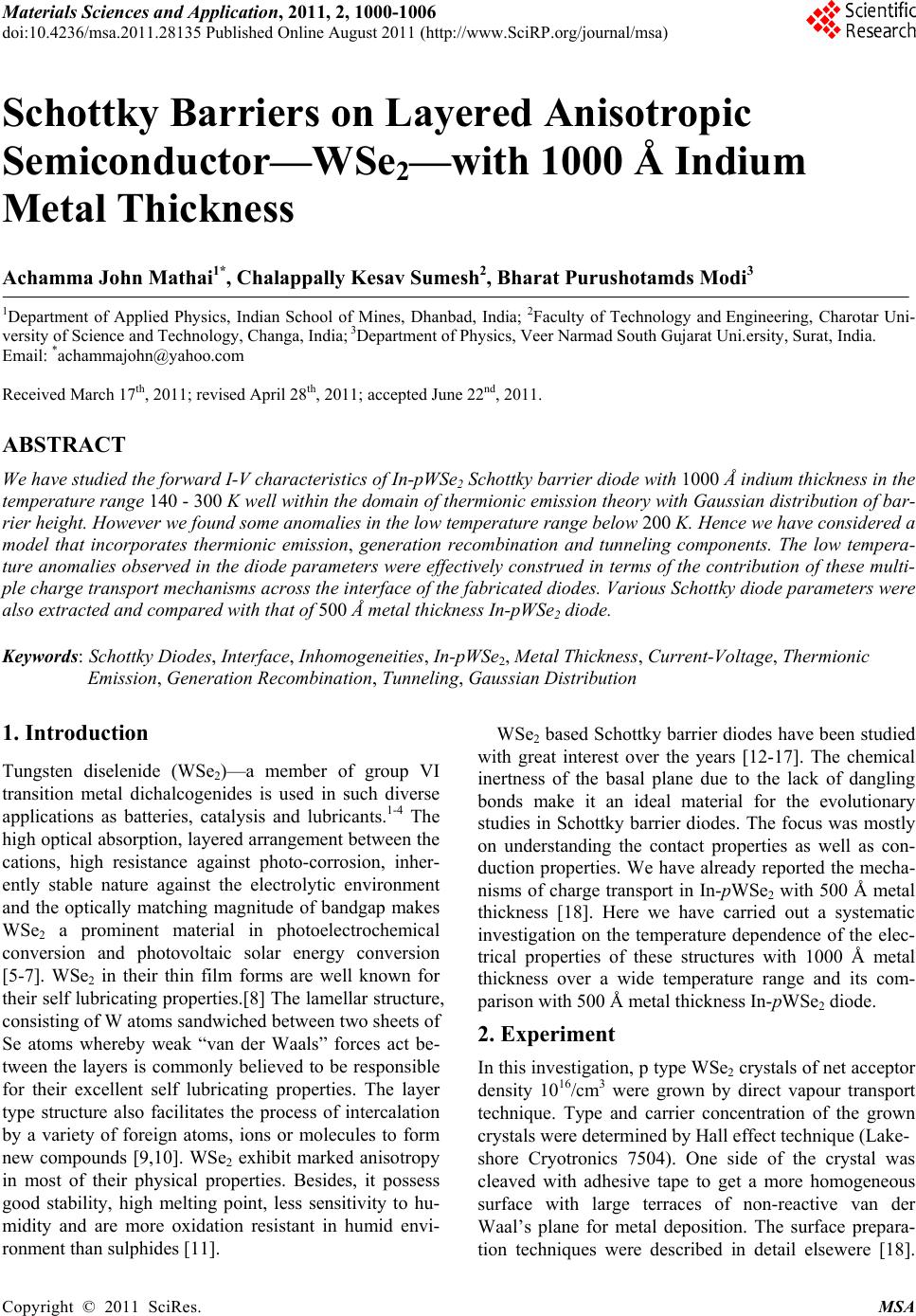 Materials Sciences and Applicatio n, 2011, 2, 1000-1006 doi:10.4236/msa.2011.28135 Published Online August 2011 (http://www.SciRP.org/journal/msa) Copyright © 2011 SciRes. MSA Schottky Barriers on Layered Anisotropic Semiconductor—WSe2—with 1000 Å Indium Metal Thickness Achamma John Mathai1*, Chalappally Kesav Sumesh2, Bharat Purushotamds Modi3 1Department of Applied Physics, Indian School of Mines, Dhanbad, India; 2Faculty of Technology and Engineering, Charotar Uni- versity of Science and Technology, Changa, India; 3Department of Physics, Veer Narmad South Gujarat Uni.ersity, Surat, India. Email: *achammajohn@yahoo.com Received March 17th, 2011; revised April 28th, 2011; accepted June 22nd, 2011. ABSTRACT We have studied the forward I-V characteristics of In-pWSe2 Schottky barrier diode with 1000 Å indium thickness in the temperature range 140 - 300 K well within the domain of thermionic emission theory with Gaussian distribution of bar- rier height. However we found some anomalies in the low temperature range below 200 K. Hence we have considered a model that incorporates thermionic emission, generation recombination and tunneling components. The low tempera- ture anomalies observed in the diode parameters were effectively construed in terms of the contribution of these multi- ple charge transport mechanisms across the interface of the fabricated diodes. Various Schottky diode parameters were also extracted and compared with that of 500 Å metal thickness In-pWSe2 diode. Keywords: Schottky Diodes, Interface, Inhomogeneities, In-pWSe2, Metal Thickness, Current-Voltage, Thermionic Emission, Generation Recombination, Tunneling, Gaussian Distribution 1. Introduction Tungsten diselenide (WSe2)—a member of group VI transition metal dichalcogenides is used in such diverse applications as batteries, catalysis and lubricants.1-4 The high optical absorption, layered arrangement between the cations, high resistance against photo-corrosion, inher- ently stable nature against the electrolytic environment and the optically matching magnitude of bandgap makes WSe2 a prominent material in photoelectrochemical conversion and photovoltaic solar energy conversion [5-7]. WSe2 in their thin film forms are well known for their self lubricating properties.[8] The lamellar structure, consisting of W atoms sandwiched between two sheets of Se atoms whereby weak “van der Waals” forces act be- tween the layers is commonly believed to be responsible for their excellent self lubricating properties. The layer type structure also facilitates the process of intercalation by a variety of foreign atoms, ions or molecules to form new compounds [9,10]. WSe2 exhibit marked anisotropy in most of their physical properties. Besides, it possess good stability, high melting point, less sensitivity to hu- midity and are more oxidation resistant in humid envi- ronment than sulphides [11]. WSe2 based Schottky barrier diodes have been studied with great interest over the years [12-17]. The chemical inertness of the basal plane due to the lack of dangling bonds make it an ideal material for the evolutionary studies in Schottky barrier diodes. The focus was mostly on understanding the contact properties as well as con- duction properties. We have already reported the mecha- nisms of charge transport in In-pWSe2 with 500 Å metal thickness [18]. Here we have carried out a systematic investigation on the temperature dependence of the elec- trical properties of these structures with 1000 Å metal thickness over a wide temperature range and its com- parison with 500 Å metal thickness In-pWSe2 diode. 2. Experiment In this investigation, p type WSe2 crystals of net acceptor density 1016/cm3 were grown by direct vapour transport technique. Type and carrier concentration of the grown crystals were determined by Hall effect technique (Lake- shore Cryotronics 7504). One side of the crystal was cleaved with adhesive tape to get a more homogeneous surface with large terraces of non-reactive van der Waal’s plane for metal deposition. The surface prepara- tion techniques were described in detail elsewere [18]. 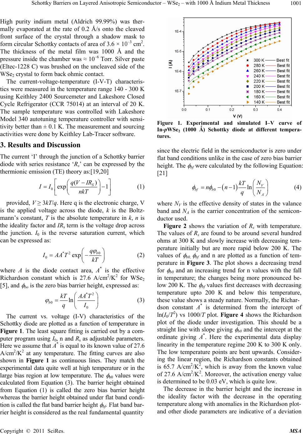 Schottky Barriers on Layered Anisotropic Semiconductor – WSe – with 1000 Å Indium Metal Thickness1001 2 High purity indium metal (Aldrich 99.99%) was ther- mally evaporated at the rate of 0.2 Å/s onto the cleaved front surface of the crystal through a shadow mask to form circular Schottky contacts of area of 3.6 × 10⁻³ cm2. The thickness of the metal film was 1000 Å and the pressure inside the chamber was ≈ 10–6 Torr. Silver paste (Eltec-1228 C) was brushed on the uncleaved side of the WSe2 crystal to form back ohmic contact. The current-voltage-temperature (I-V-T) characteris- tics were measured in the temperature range 140 - 300 K using Keithley 2400 Sourcemeter and Lakeshore Closed Cycle Refrigerator (CCR 75014) at an interval of 20 K. The sample temperature was controlled with Lakeshore Model 340 autotuning temperature controller with sensi- tivity better than ± 0.1 K. The measurement and sourcing activities were done by Keithley Lab-Tracer software. 3. Results and Discussion The current ‘I’ through the junction of a Schottky barrier diode with series resistance ‘Rs’ can be expressed by the thermionic emission (TE) theory as:[19,20] 0 () exp 1 S qV IR II nkT (1) provided, V ≥ 3kT/q. Here q is the electronic charge, V is the applied voltage across the diode, k is the Boltz- mann’s constant, T is the absolute temperature in k, n is the ideality factor and IRs term is the voltage drop across the junction. I0 is the reverse saturation current, which can be expressed as: *2 0 0exp b q IAAT kT (2) where A is the diode contact area, A* is the effective Richardson constant which is 27.6 A/cm2/K2 for WSe2 [5], and bo is the zero bias barrier height, expressed as: *2 0 0 ln b kTAA T qI (3) The current vs. voltage (I-V) characteristics of the Schottky diode are plotted as a function of temperature in Figure 1. The least square fitting is carried out by a com- puter program using I0, n and Rs as adjustable parameters. Here we assume that A* is equal to its known value of 27.6 A/cm2/K2 at any temperature. The fitting curves are also shown in Figure 1 as continuous lines. They match the experimental data quite well at high temperature or in the large bias region at low temperature. The b0 values were calculated from Equation (3). The barrier height obtained from Equation (1) is called the zero bias barrier height whereas the barrier height obtained under flat band condi- tion is called the flat band barrier height bf. Flat band bar- rier height is considered as the real fundamental quantity Figure 1. Experimental and simulated I–V curve of In-pWSe2 (1000 Ǻ) Schottky diode at different tempera- tures. since the electric field in the semiconductor is zero under flat band conditions unlike in the case of zero bias barrier height. The bf were calculated by the following Equation: [21] 01ln V bf b A N kT nn qN (4) where NV is the effective density of states in the valance band and NA is the carrier concentration of the semicon- ductor used. Figure 2 shows the variation of Rs with temperature. The values of Rs are found to be around several hundred ohms at 300 K and slowly increase with decreasing tem- perature initially but are more rapid below 200 K. The values of b0, bf and n are plotted as a function of tem- perature in Figure 3. The plot shows a decreasing trend for b0 and an increasing trend for n values with the fall in temperature; the changes being more pronounced be- low 200 K. The bf values first decreases with decreasing temperature upto 200 K and below this temperature, these value shows a steady nature. Normally, the Richar- dson constant A* is determined from the intercept of ln(I0/T2) vs 1000/T plot. Figure 4 shows the Richardson plot of the diode under investigation. This should be a straight line with slope giving b0 and the intercept at the ordinate giving A*. Here the experimental data display linearity in the temperature regime 200 K to 300 K only. The low temperature points are bent upwards. Consider- ing the linear region, the Richardson constants obtained is 65.7 A/cm2/K2, which is away from the known value of 27.6 A/cm2/K2. Moreover, the activation energy value is determined to be 0.03 eV, which is quite low. The decrease in the barrier height and the increase in the ideality factor with the decrease in the operating temperature along with anomalies in the Richardson plot- and other diode parameters are indicative of a deviation Copyright © 2011 SciRes. MSA 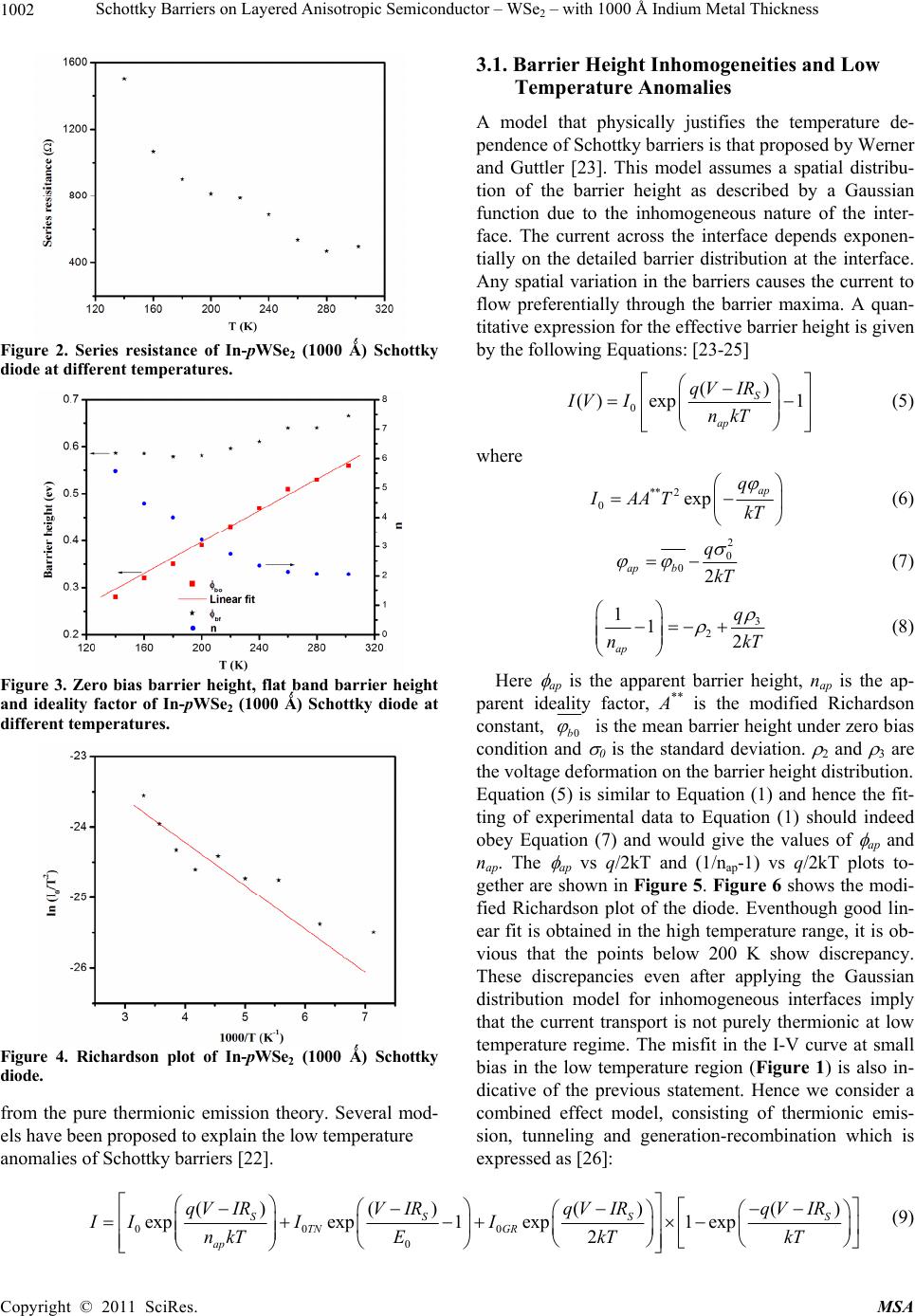 Schottky Barriers on Layered Anisotropic Semiconductor – WSe2 – with 1000 Å Indium Metal Thickness Copyright © 2011 SciRes. MSA 1002 3.1. Barrier Height Inhomogeneities and Low Temperature Anomalies A model that physically justifies the temperature de- pendence of Schottky barriers is that proposed by Werner and Guttler [23]. This model assumes a spatial distribu- tion of the barrier height as described by a Gaussian function due to the inhomogeneous nature of the inter- face. The current across the interface depends exponen- tially on the detailed barrier distribution at the interface. Any spatial variation in the barriers causes the current to flow preferentially through the barrier maxima. A quan- titative expression for the effective barrier height is given by the following Equations: [23-25] Figure 2. Series resistance of In-pWSe2 (1000 Ǻ) Schottky diode at different temperatures. 0 () () exp1 S ap qV IR IV InkT (5) where ** 2 0exp ap q IAAT kT (6) 2 0 02 ap b q kT (7) 3 2 112 ap q nkT (8) Here ap is the apparent barrier height, nap is the ap- parent ideality factor, A** is the modified Richardson constant, 0b is the mean barrier height under zero bias condition and 0 is the standard deviation. 2 and 3 are the voltage deformation on the barrier height distribution. Figure 3. Zero bias barrier height, flat band barrier height and ideality factor of In-pWSe2 (1000 Ǻ) Schottky diode at different temperatures. Equation (5) is similar to Equation (1) and hence the fit- ting of experimental data to Equation (1) should indeed obey Equation (7) and would give the values of ap and nap. The ap vs q/2kT and (1/nap-1) vs q/2kT plots to- gether are shown in Figure 5. Figure 6 shows the modi- fied Richardson plot of the diode. Eventhough good lin- ear fit is obtained in the high temperature range, it is ob- vious that the points below 200 K show discrepancy. These discrepancies even after applying the Gaussian distribution model for inhomogeneous interfaces imply that the current transport is not purely thermionic at low temperature regime. The misfit in the I-V curve at small bias in the low temperature region (Figure 1) is also in- dicative of the previous statement. Hence we consider a combined effect model, consisting of thermionic emis- sion, tunneling and generation-recombination which is expressed as [26]: Figure 4. Richardson plot of In-pWSe2 (1000 Ǻ) Schottky diode. from the pure thermionic emission theory. Several mod- els have been proposed to explain the low temperature anomalies of Schottky barriers [22]. 00 0 0 () ()()() expexp1exp1 exp 2 SS S TN GR ap qVIR VIRqVIRqVIR II II n kTEkTkT S (9)  Schottky Barriers on Layered Anisotropic Semiconductor – WSe – with 1000 Å Indium Metal Thickness 1003 2 Figure 5. ap and (1/nap−1) vs q/2kT plot of In-pWSe2 (1000 Ǻ) Schottky diode. Figure 6. Modified Richardson plot of In-pWSe2 (1000 Ǻ) Schottky diode. where I0TN and I0GR are the tunneling and generation re- combination saturation current respectively. E 0 is the tunneling parameter described elsewere [19,20]. All the other terms have their usual meaning. Now the low temperature I-V curve for 140, 160 and 180 K is simulated with Equation (9) and is shown in Figure 7, which seems to be excellent with Equation (9). New values of I0 and nap were extracted from Equation (9) and ap were recalculated for these temperatures. Now using the new values of ap and nap, Figure 5 gives a straight line over the whole temperature range. Likewise, by the new I0 values, the modified Richardson plot also is a straight line over the entire temperature range (Figure 6). The values of 0b and 0 were determined as 0.87 eV and 0.128 eV respectively from the linear fit of ap vs q/2kT plot .By the linear fit of nap vs q/2kT plot, 2 and 3 were obtained as 0.114 eV and -0.019 eV respectively. Similarly, the modified Richardson constant A** and the mean barrier height 0b were extracted from the linear fit of the modified Richardson plot. The A** value of 22.8 Figure 7. Experimental and simulated forward I–V curve of In-pWSe2 (1000 Ǻ) Schottky diode at 180, 160 and 140 K temperatures. A/cm2/K2 is in a closer agreement with the known value of 27.6 A/cm2/K2. Moreover, 0b value was found to be 0.87 eV, which matches exactly with that of ap vs q/2kT plot. The inhomogeneity calculated for this diode is 14.7% which is rather high. Due to the specific nature of WSe2 surface [27-29] inhomogeneities in various forms can be readily expected at the In-pWSe2 interface. This may be one of the reasons for the large values of n. High values of n also indicate the voltage dependence of barrier height. Such behaviors occur when the barrier heights vary laterally and the dimensions of these inho- mogeneities are in the order of the depletion layer width. Now, ap and nap vs T were plotted according to Equa- tions (7) and (8) in the whole temperature range with their new values at temperatures 140, 160 & 180 K (Figure 8). We can see that the theoretical curve closely follows the experimental data. The voltage sensitivity of the barrier height distribu- tion and standard deviation was investigated for two bi- Figure 8. Measured and simulated barrier height and ideal- ity factor of In-pWSe2 (1000 Ǻ) Schottky diode based on Equations (7) and (8). Copyright © 2011 SciRes. MSA 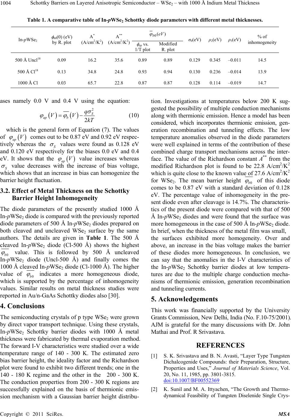 Schottky Barriers on Layered Anisotropic Semiconductor – WSe – with 1000 Å Indium Metal Thickness 1004 2 Table 1. A comparative table of In-pWSe2 Schottky diode parameters with different metal thicknesses. 0() beV In-pWSe2 b0(0) (eV) by R. plot A* (A/cm2/K2) A** (A/cm2/K2) ap vs. 1/T plot Modified R. plot σ0(eV) ρ2(eV) ρ3(eV) % of inhomogeneity 500 Å Uncl18 0.09 16.2 35.6 0.89 0.89 0.129 0.345 –0.011 14.5 500 Å Cl18 1000 Å Cl 0.13 0.03 34.8 65.7 24.8 22.8 0.93 0.87 0.94 0.87 0.130 0.128 0.236 0.114 –0.014 –0.019 13.9 14.7 ases namely 0.0 V and 0.4 V using the equation: 2 2 S ap b q VV kT (10) which is the general form of Equation (7). The values of comes out to be 0.87 eV and 0.92 eV respec- tively whereas the S ap V values were found as 0.128 eV and 0.120 eV respectively for the biases 0.0 eV and 0.4 eV. It shows that the value increases whereas S ap V value decreases with the increase of bias voltage, which shows that an increase in bias can homogenize the barrier height fluctuation. 3.2. Effect of Metal Thickness on the Schottky Barrier Height Inhomogeneity The diode parameters of the presently studied 1000 Å In-pWSe2 diode is compared with the previously reported diode parameters of 500 Å In-pWSe2 diodes prepared on both cleaved and uncleaved WSe2 surface by the same authors. The details are given in Table 1. The 500 Å cleaved In-pWSe2 diode (Cl-500 Å) shows the highest 0b value. This is followed by 500 Å uncleaved In-pWSe2 diode (Uncl-500 Å) and finally comes the 1000 Å cleaved In-pWSe2 diode (Cl-1000 Å). The higher value of 0b indicates a more homogeneous diode, which is supported by the percentage of inhomogeneity values. Similar results on metal thickness studies were reported in Au/n-GaAs Schottky diodes also [30]. 4. Conclusions The semiconducting crystals of p type WSe2 were grown by direct vapor transport technique. Using these crystals, In-pWSe2 Schottky barrier diodes with 1000 Å metal thickness were fabricated by thermal evaporation method. The forward I-V characteristics were studied over a wide temperature range of 140 - 300 K. The estimated zero bias barrier height, the ideality factor and the Richardson plot were found to exhibit two different trends; one in the 140 - 180 K regime and the other in the 200 - 300 K. The conduction properties from 200 - 300 K regions are successfully explained on the basis of thermionic emis- sion mechanism with a Gaussian barrier height distribu- tion. Investigations at temperatures below 200 K sug- gested the possibility of multiple conduction mechanisms along with thermionic emission. Hence a model has been considered, which incorporates thermionic emission, gen- eration recombination and tunneling effects. The low temperature anomalies observed in the diode parameters were well explained in terms of the contribution of these combined charge transport mechanisms across the inter- face. The value of the Richardson constant A** from the modified Richardson plot is found to be 22.8 A/cm2/K2 which is quite close to the known value of 27.6 A/cm2/K2 for WSe2. The mean barrier height 0b of this diode comes to be 0.87 eV with a standard deviation of 0.128 eV. The percentage value of inhomogeneity in the pre- sent diode even after cleavage is 14.7%. The characteris- tics of the present diode were compared with that of 500 Å In-pWSe2 diodes and were found that the surface was more homogeneous in the case of 500 Å In-pWSe2 diode. In brief, when the thickness of the metal film was small, the surfaces exhibited more homogeneity. Over and above, an increase in the bias voltage makes the barrier of these diodes more homogeneous. In conclusion, we can say that the anomalies in the I-V characteristics of the In-pWSe2 Schottky barrier diodes at low tempera- tures are due to the multiple charge conduction mecha- nisms of thermionic emission, generation recombination and tunneling currents. 5. Acknowledgements This work was financially supported by the University Grants Commission, New Delhi, India (No. F.10-75/2001). AJM is grateful for the many discussions with Dr. John Mathai and Prof. R Srivastava. REFERENCES [1] S. K. Srivastava and B. N. Avasti, “Layer Type Tungsten Dichalcogenide Compounds: their Preparation, Structure, Properties and Uses,” Journal of Materials Science, Vol. 20, No. 11, 1985, pp. 3801-3815. doi:10.1007/BF00552369 [2] K. Sunil and M. A. Ittyachen, “The Growth and Thermo- dynamical Feasibility of Tungsten Diselenide Single Crys- Copyright © 2011 SciRes. MSA  Schottky Barriers on Layered Anisotropic Semiconductor – WSe – with 1000 Å Indium Metal Thickness1005 2 tals Using Chemical Vapour Transport Technique,” Bul- letin of Materials Science, Vol. 20, No. 2, April 1997, pp. 231-238. doi:10.1007/BF02744893 [3] H. Ogawa, A. Iwamae, T. Sugie, S. Kasai, Y. Kawano, S. Kajita and Y. Kusama, “Research and Development of Optical Diagnostics for ITER,” Proceedings of 22nd Fu- sion Energy Conference (FEC 2008)”, Geneva, 13-18 October 2008. [4] V. Podzorov, M. E. Gershenson, C. Kloc, R. Zeis and E. Bucher, “High-mobility Field-effect Transistors Based on Transition Metal Dichalcogenides,” Applied Physics Let- ters, Vol. 84, No. 17, April 2004, pp. 3301-3303. doi:10.1063/1.1723695 [5] A. Klein, Y. Tomm, R. Schlaf, C. Pettenkofer, W. Jae- german, M. Lux-Steiner and E. Bucher, “Photovoltaic Properties of WSe2 Single Crystals Studied by Photoelec- tron Spectroscopy,” Solar Energy Material and Solar Cell, Vol. 51, No. 2, 24 February 1998, pp. 181-191. doi:10.1016/S0927-0248(97)00234-1 [6] G. A. Scholz and H. Gerisher, “Voltage Distribution at the N-WSe2 and N-MoSe2 Electrolyte Interface,” Journal of the Electrochemical Society, Vol. 139, 1992, pp. 165- 170. doi:10.1149/1.2069164 [7] S. Akari, M. Ch. Lux-Steiner, K. Glockler, T. Schill, R. Heitkamp, B. Koslowski and K. Dransfeld, “Photovoltaic Characterization of WSe2 with the Scanning Tunneling Microscope,” Annalen der Physik., Vol. 505, No. 2, 1993, pp. 141-148. doi:10.1002/andp.19935050206 [8] A. Pauschit, E. Badisch, M. Roy and D. V. Shtansky, “On the Scratch Behaviour of Self-lubricating WSe2 Films,” Wear, Vol. 267, No. 11, 29 October 2009, pp. 1909-1914. doi:10.1016/j.wear.2009.03.037 [9] M. Kamaratos, C. A. Papageorgopoulos, D. C. Papa- georgopoulos, W. Jaegermann, C. Pettenkofer and J. Lehmann, “Adsorption of Br2 on Na-intercalated NWSe2: Br-induced Deintercalation,” Surface Science, Vol. 377- 379, 20 April 1997, pp. 659-663. doi:10.1016/S0039-6028(96)01474-4 [10] M. Kamaratos, V. Saltas, C. A. Papageorgopoulos, W. Jaegermann, C. Pettenkofer and D. Tonti, “Interaction of Na and Cl2 on WSe2(0001) Surfaces: Chlorine-induced Na Deintercalation,” Surface Science, Vol. 402-404, 1998, pp. 37-41. doi:10.1016/S0039-6028(97)00906-0 [11] D. V. Shtansky, T. A. Lobova, V. Yu Fominisky, S. A. Kulinich, I. V. Lyasotsky, M. I. Petrzluk, E. A. Levashow and J. J. Moore, “Structure and Tribological Properties of WSex, WSex/TiN, WSex/TiCN and WSex/TiSiN Coat- ings,” Surface and Coatings Technology, Vol. 183, No. 2-3, 24 May 2004, pp. 328-336. doi:10.1016/j.surfcoat.2003.09.047 [12] C. A. Papageorgopoulos, M. Kamaratos and A. Papa- georgopoulos, “Adsorption of Cs on WSe2 Van Der Waals Surfaces: Temperature and Sputter Effects on Growth Properties,” Surface Science, Vol. 275, No. 3, 15 September 1992, pp. 314-322. doi:10.1016/0039-6028(92)90803-E [13] R. Schlaf, A. Klein, C. Pettenkofer and W. Jaegermann, “Laterally Inhomogeneous Surface-Potential Distribution and Photovoltage at Clustered In/WSe2(0001) Interfaces,” Physical Review B, Vol. 48, No. 19, 15 November 1993, pp. 14242-14252. doi:10.1103/PhysRevB.48.14242 [14] A. Klein, C. Pettenkofer, W. Jaegermann, M. Lux-Steiner and E. Bucher, “A Photoemission Study of Barrier and Transport Properties of the Interfaces of Au and Cu with WSe2(0001) Surfaces,” Surface Science, Vol. 321, No. 1-2, 10 December 1994 , pp. 19-31. doi:10.1016/0039-6028(94)90023-X [15] S. D. Foulias, D. S. Vlachos, C. A. Papageorgopoulos, R. Yavor, C. Pettenkofer and W. Jaegermann, “A Synchro- tron Radiation Study of the Interaction of Na with WSe2 and TaSe2: Oxygen-Induced Deintercalation,” Surface Science, Vol. 352-354, 1996, pp. 463-467. doi:10.1016/0039-6028(95)01180-3 [16] A. Rettenberger, P. Bruker, M. Metzler, F. Mugele, T. W. Matthes, M. Bohmisch, J. Boneberg, K. Friemelt and P. Leiderer, “STM Investigation of the Island Growth of Gold on WS2 and WSe2, ” Surface Science, Vol. 402-404, 15 May 1998, pp. 409-412. doi:10.1016/S0039-6028(97)00961-8 [17] G. Nicolay, R. Claessen, F. Reinert, V. N. Strocov, S. Hufner, H. Gao, U. Hartmann and E. Bucher, “Fast Epi- taxy of Au and Ag on WSe2,” Surface Science, Vol. 432, No. 1-2, 9 July 1999, pp. 95-100. doi:10.1016/S0039-6028(99)00520-8 [18] A. J. Mathai and K. D. Patel, “Schottky Diode Character- istics: Aluminium with 500 and 1000 Ǻ Thicknesses on P type WSe2 Crystal,” Crystal Research and Technology, Vol. 45, No. 7, 2010, pp. 717-724. doi:10.1002/crat.201000172 [19] E. H. Rhoderick and R. H. Williams, “Metal-Semicon- ductor Contacts,” 2nd Edition, Clarendon Press, Oxford, 1988. [20] S. M. Sze, “Physics of Semiconductor Devices,” 2nd Edition, Wiley, New York, 1981. [21] L. F. Wagner, R. W. Young and A. Sugerman, “A Note on the Correlation between the Schottky Diode Barrier Height and the Ideality Factor as Determined from I-V Measurements,” IEEE Electron Device Letters, Vol. 4, No. 4, April, 1983, pp. 320-322. doi:10.1109/EDL.1983.25748 [22] R. Sharma, “Temperature Dependence of I-V Character- istics of Au/n-Si Schottky Barrier Diode,” Journal of Electron Devices, Vol. 8, 2010, pp. 286-292. [23] J. H. Werner and H. H. Guttler, “Barrier Inhomogeneities at Schottky Contacts,” Journal of Applied Physics, Vol. 69, No. 3, 1991, pp. 1522-1533. doi:10.1063/1.347243 [24] S. Chand and J. Kumar, “Effect of Barrier Height Distri- bution on the Behaviour of a Schottky Diode,” Journal of Applied Physics, Vol. 82, No. 10, November 1997, pp. 5005-5010. doi:10.1063/1.366370 [25] Y. P. Song, R. L. Van Meirhaeghe, W. H. Laflere and F. Cardon, “On the Difference in Apparent Barrier Height as Obtained from Capacitance-voltage and Current-voltage- temperature Measurements on Al/p-InP Schottky Barri- ers,” Solid-State Electronics, Vol. 29, No. 6, June 1986, Copyright © 2011 SciRes. MSA  Schottky Barriers on Layered Anisotropic Semiconductor – WSe2 – with 1000 Å Indium Metal Thickness Copyright © 2011 SciRes. MSA 1006 pp. 633-638. doi:10.1016/0038-1101(86)90145-0 [26] D. Donoval, D. Vladimir and L. Marek, “A Contribution to the Analysis of the I-V Characteristics of Schottky Structures,” Solid-State Electronics, Vol. 42, No. 2, 16 March 1998, pp. 235-241. doi:10.1016/S0038-1101(97)00237-2 [27] D. Mahalu, A. Jakubowicz, A. Wold and R. Tenne, “Pas- sivation of Recombination Centers on theWSe2 Surface,” Physical Review B, Vol. 38, No. 2, July 15 1988, pp. 1533-1536. doi:10.1103/PhysRevB.38.1533 [28] P. Salvador, M. Pujadas and G. Campet, “Photoreactions at the N-type-WSe2–electrolyte Interface: Study by Elec- trolyte Electroreflectance and Photocurrent Transient Measurements,” Physical Review B, Vol. 38, No. 14, 15 November 1988, pp. 9881-9888. doi:10.1103/PhysRevB.38.9881 [29] A. Jacubowicz, D. Mahalu, M. Wolf, A. Wold and R. Tenne, “WSe2: Optical and Electrical Properties as Re- lated to Surface Passivation of Recombination Centers,” Physical Review B, Vol. 40, No. 5, 15 August 1989, pp. 2992-3000. doi:10.1103/PhysRevB.40.2992 [30] M. Biber, O. Gullu, S. Forment, R. L. V. Meirhaeghe and A. Turut, “The Effect of Schottky Metal Thickness on Barrier Height Inhomogeneity in Identically Prepared Au/n-GaAs Schottky Diodes,” Semiconductor Science and Technology, Vol. 21, No. 1, 2006, pp. 1-5. doi:10.1088/0268-1242/21/1/001 |