 Circuits and Systems, 2016, 7, 630-642 Published Online May 2016 in SciRes. http://www.scirp.org/journal/cs http://dx.doi.org/10.4236/cs.2016.76054 How to cite this paper: Saravanan, S., Vennila, I. and Mohanram, S. (2016) Design and Implementation of Efficient Reversi- ble Arithmetic and Logic Unit. Circuits and Systems, 7, 630-642. http://dx.doi.org/10.4236/cs.2016.76054 Design and Implementation of Efficient Reversible Arithmetic and Logic Unit Subramanian Saravanan1*, Ila Venni la1, Sudha Mohanram2 1Department of EEE, P. S. G. College of Technology, Coimbatore, India 2Sri Eshwar College of Engineering, Kondampatty, Coimbatore, India Received 11 March 2016; accepted 6 May 2016; published 11 May 2016 Copyright © 2016 by authors and Scientific Research Publishing Inc. This work is licensed under the Creative Commons Attribution International License (CC BY). http://creativ ecommon s.org/l icenses/by /4.0/ Abstract In computing architecture, ALU plays a major role. Many promising applications are possible with ATMEGA microcontroller. ALU is a part of these microcontrollers. The performance of these mi- crocontrollers can be improved by applying Reversible Logic and Vedic Mathematics. In this paper, an efficient reversible Arithmetic and Logic Unit with reversible Vedic Multiplier is proposed and the simulation results show its effectiveness in reducing quantum cost, number of gates, and the total number of logical calculations. Keywords Reversible Logic Gates, Reversible Logic Circuits, Reversible Multiplier Circuits, Vedic Multiplier, ALU 1. Introduction Moore’s law states that number of transistors in a chip doubles every two years but chip size decreases. This cannot be reduced greatly which will lead to more power consumption. This paves the path to ne w technologies “Reversible Logic ” and “Quantum Dot Cell ular Automata” (QCA). As stated b y Launder irreversible logic (un- equal number of inputs and outputs) consumes more power [1]. To overcome this problem Bennett sets equal number of inputs and outputs, which will dissipate less po wer as input bits are preserved at the output [2]. T his is called Reversible Logi c. I n this p ap er , Reversible Lo gic is chosen for its low power and Vedic concept is used for its faster arithmetic calculations. A quantum computer uses principle of superposition and entangleme nt for qubit (quantum bit-basic unit of information in quantu m computers) computation. Quantum computers are faster than classical computer and will find its application in air craft tester, driverless cars and develop more effective * 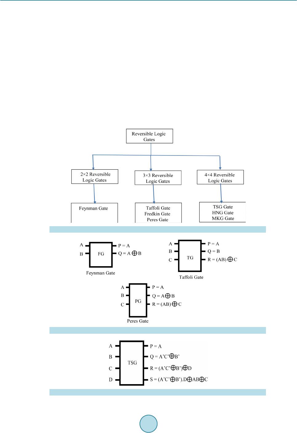 S. Saravanan et al. drugs, etc. Reversible Logic plays an important role in converting classical computation to quantum computa- tion. The b a sic properties of Re ver sib le Logic are discussed in [3]. Reversible gates are classified as 2 × 2 gates, 3 × 3 gates and 4 × 4 gates. The classification of Reversible Logic gates is given in Figure 1. The basic reversible gates are Feynman gate, Taffoli gate and Peres gate. The basic reversible gates are shown in Figure 2 [4]. The 4 × 4 reversible gates such as TSG gate and HNG gate are discussed in [3] given below. TSG Gate Thapliyal proposed a 4 × 4 reversible gate called TSG gate [5]. The TSG gate is shown in Figure 3 and quantum circuit diagram for TSG gate is given in Figure 4. The input and output functions are given i n Equa- tions (1) and (2) respectively. (1) () () ( ) Ov PA,QAC B,RAC BD,SAC BDABC ′′ ′′′ ′′′ ′ = ==⊕=⊕⊕=⊕⋅⊕⊕ (2) Full adder, Wallace tree multiplier 4:2 compressor are constructed using TSG gate. Figure 1 . Classification of reversible logic gates. Figure 2 . Bas ic reversible gat es . Figure 3 . T SG gate. 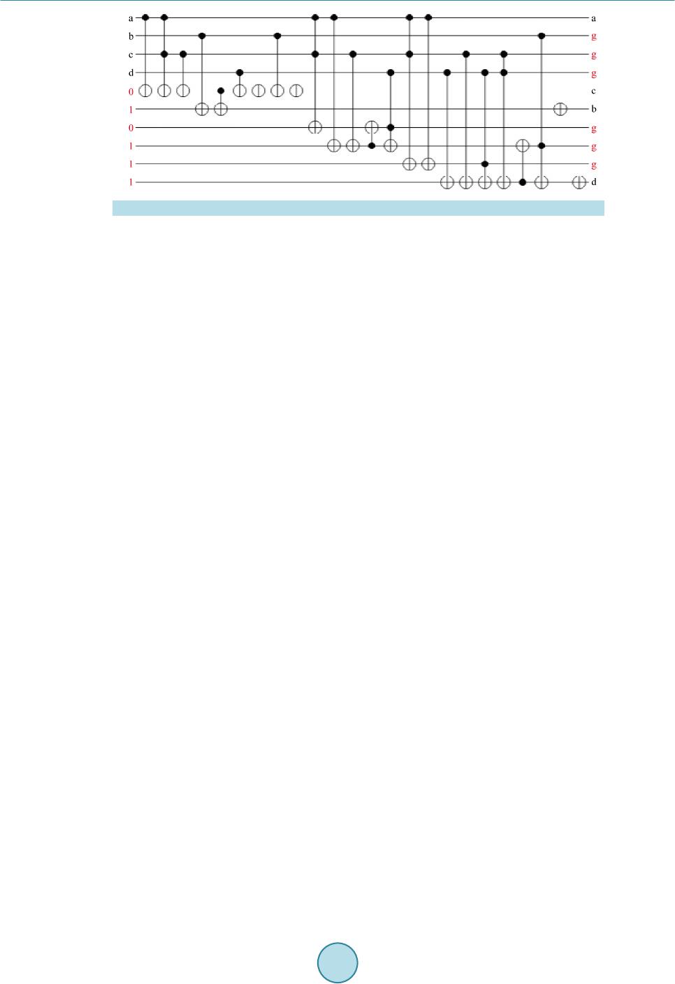 S. Saravanan et al. Figure 4 . Quantum circuit diagram for TSG gate. Single TSG gate will act as full adder. Parallel adder or ripple carry adder is implemented using the same. Ripple carry adder is needed in multiplier. When C input is 0, D input is given with carry input, and then TSG gate functions as full adder. The TSG gate as full adder is shown in Figure 5. HNG Gate It is a 4 × 4 reversible gate [6]. The HNG gate is shown in Figure 6 and quantum circuit diagram for HNG gate is given in Figure 7. The input and outp ut func tions are given in Equa tions (3) and (4) respectively. (3) ( ) () OvPA,QB,RABC,S ABCABD ==== ⊕⊕=⊕⊕⊕ (4) HNG ga te is use d to c onstruc t full adder and multiplier. When D input is 0, A, B and C in puts ar e give n, and then HNG gate functions as full adder. The HNG gate as full adder is shown in Figure 8. The basic benchmark parameters of the reversible logic circuits are quantum cost, garbage output, and total number of logical calculations . The nu mber o f reversible logic gates either 1 × 1, 2 × 2, 3 × 3 or 4 × 4 needed to design a reversible system is called number of gates. Quantum cost (QC) refers to the number of elementary gates 1 × 1 or 2 × 2 reversible logic gates needed to design the reversible logic circuit. The unused output in a reversible circuit is called garbage output. Tota l logic calculation is the n umber o f XO R, AND, and N OT logic functio ns used i n the re versible cir c uit. α indicates number of XOR logic in the circuit, β indicates number of AND logic in the circuit and d indicates number of NOT logic in the circui t Research in reversible logic is getting important today. Thapliyal and Srinivasan proposed a new reversible TSG gate [5] and d is cussed about reversible carry look-ahead adder and other adder architecture which formed a part of ALU. The quantum cost of TSG gate is quiet high when compared to HNG gate. Haghparast proposes two new 4 × 4 bit reversible multiplier designs with less hardware complexity, less garbage bits, less quantum cost, and le ss co nsta nt inp uts [6] and the architecture uses Peres gate for partial product generation. But the total logical calculation is more due to extra logics in Peres gate. Research is going on in deriving more applications out of it. Research is moving towards deriving a new application from reversible gates. Ancient Indians fol- lowed some sutras or formulae for mathematical computation. These basic mathematical calculations form the base for modern VLSI architecture. Thapliyal discussed about performance of Vedic Multipliers on FPGA [7] and discussed the irreversible architecture based on delay. These architectures when implemented in VLSI will reduce power consumption. Ehsan Pour Ali Akbar et al. proposed reversible signed Wallace tree multiplier in [8]. Synthesis of reversible c i rcuits is discussed in [9]-[14] and testing of reversible circuits is discussed in [15]. 1.1. Vedic Multiplication “Vedic Mathematics” was derived fro m the ancient word “Vedas”. Vedic mathematics was rediscovered in early twentieth century. It works on the sixteen mathematical formulae called as “sutras” [16]. Mostly the speed of the DSP processors depends mainly on the speed of its multipliers which in turn depends on number of internal log- ics used [17]. Multipliers are used to realize many important functions such as Fast Fourier transforms and con- 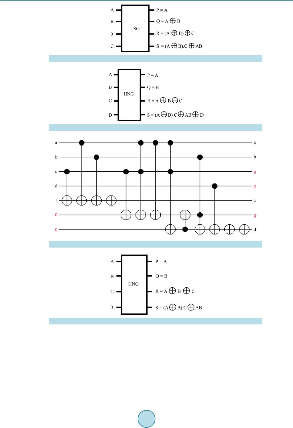 S. Saravanan et al. Figure 5 . TSG gat e as full adder. Figure 6 . HNG gate. Figure 7 . Quantum circu it diagram for HNG gate. Figure 8 . HNG gate as full adder. volutions. VLSI architectures built using these sutras will improve the performance of the system. Vedic ma- thematics makes complex conventional calculations to be simpler and easier ones [18]. I t does the computatio ns very fast using h uman mind. Ved ic Mathematics is a set of arithmetic rules that allo ws more efficient and spee- dy calculatio ns. “Urdh va Tirya gbhyam” and “Nikhilam Navatashcaramam Dashatah” are the two important su- tras involved i n multiplication . Conventionall y these Sutras are used to multiply dec imal numbers. In this pa per these sutras were applied to binary number system which makes it compatible for digital hardware. The partial products are generated in parallel but there will be some delay due to propagation of carry. It requires less hard- ware to implement. 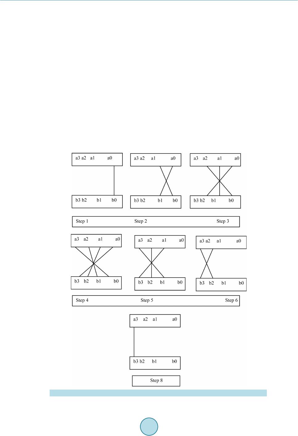 S. Saravanan et al. 1.2. Urdhva Tiryagbhyam Sutra The Vedic Multiplier is designed using Urdh va Tiryagbhyam Sutra. This sutra has b e e n traditionally used for the multiplication of two numbers. Urdhva Tiryagbhyam Sutra means “Vertically and Crosswise” [19]. The Least significant bits and most significant bits are multiplied vertically. LSB and MSB bits are multiplied crosswise and added as well. The line di agra m for Urd hva T ir yagb hya m Sutr a (step sequence from step 1 to step 7) is dis- cussed in [3] and shown in Fig ure 9. Tiwari et al. discussed about various Vedic Multipliers [20]. Rong Lin proposed reconfigurable and self-re- pairable multipliers and discussed about recursive architecture decomposition of partial product matrices [21]. Deodhe et al. presented a design of 8 bit Vedic Multiplier usin g CMOS lo gic [22]. Kuma r et al. demonstrated 8 bit Vedic Multiplier usi ng ba r rel s hifte r [23]. Haghparast’s parity preserving reversible Vedic Multiplier has ad- vantage of concurrent te s ting but its quantu m cost is high [24]. Saravanan et al. discussed about reversible Vedic Multiplier d esign usi ng ni khilam sutra [25]. 2. Proposed Reversible ALU ALU forms the major part of any processor. In this paper a reversible ALU is designed. All components of ALU are reversible in nature (equal inputs and outputs). Furthermore Vedic concept is adopted to enhance the speed of the processor by reducing critical path delay. The reversible ALU consists of 8 bit Multiplier, Logical unit and Binary to gray code converter. The sub modules are discussed below. Figure 9 . Line diagram for Urdhva Tiryagbhyam Su tra (step sequence from step1 to step7).  S. Saravanan et al. 2.1. Vedic Multiplier The 8 × 8 Vedic multiplier can be built fro m 2 × 2 Vedic multiplier. 8 × 8 Vedic multip lier require s 16 × 2 × 2 Vedic multiplier. 2 × 2 Vedic multiplier requires 4 multiplications and 2 half additions. To implement 8 × 8 Vedic multiplier it requires 64 multiplications and 32 half additions and 16 full additions. In contrast conven- tional array multiplier requires 64 multiplications and 50 full adders. So hardware complexity can be reduced using Vedic multipliers. Consider two numbers with equal MSB and they are placed at equal distance from median value is taken. For this case if the i np ut is t a ken in BCD form ei ght 2 × 2 Vedic multipliers and 8 bit adders are required. It requires 32 multiplications, 16 half additions and 8 full additions are required. Thus the multiplier can be implemented with less hardware architecture. Reversible 8 × 8 Vedic Multiplier Architecture The multiplier architecture is shown in Figure 10. In the prop osed multiplier firs t LSB bits of multiplicand a nd multiplier are passed on to 4 × 4 Vedic multiplier. MSB bits of multiplicand and multiplier are multiplied and the result is once again added with MSB bits of multiplicand to get MSB of results. The algorithm works only for multiplicand and multiplie r deviating from centra l value by equidistant. Multipliers uses TSG gate based reversible Vedic multiplier or HNG gate based reversible Vedic multiplier. The add er block uses 8 HNG gates. The third input of HNG gate is Carr y input. The last o utput of HNG gate is car ry o utp ut . The four t h i np ut o f HN G ga te i s “0” i np ut. T he c ar r y o utp ut is p r o pagated to next stage carr y input [3]. 2.2. Logical Unit It is an 8 bit logical unit. It consists of 8 peres gates. Peres gates generates AND logic and EXOR logic. The quantum cost of Peres gate is 4. There is only one garbage output. The Reversible logic unit architecture is shown in Fi gure 11. The inputs are A7 - A0 and B7 - B0. The input C7 - C0 is constant input which is 0. The QQ17 - QQ10 represents logical EXOR operation. The RR17 - RR10 represents logical AND operation. 2.3. Binary to Gray Code Converter Unit It is a n 8 b it bi nary to gra y code conver ter uni t. I t cons ists o f 8 Fe ynma n gate s. Fe ynman gates gener ate EX OR Figure 1 0. Multiplier architecture.  S. Saravanan et al. Figure 1 1. Reversible logic uni t architectur e. logic . T he q uantum co st of F eyn man ga te is 1 . T her e is onl y one garbage output. The Reversible Binary to Gray Code Converter Architecture is shown in Figure 12. T he inp uts to Fe ynma n gate ar e A7 - A0. I n this c urre nt bit is operate d with previous bit. The Q17 - Q1 0 represents binary to gray code converted value. 2.4. Proposed Reversible ALU Archit ect ure The ALU consists of Arithmetic unit and logic unit. The Reversible ALU architecture is shown in Figure 13. The Reversible ALU cons ists o f 8 bit re versible Ve dic multi plie r unit, re versible lo gical unit a nd rever sible 8 bit binary to gray code converter. The logical unit consists of Peres gate which generates AND logic and EXOR logic. The EXOR logic is used to perform equality checking between two data.  S. Saravanan et al. Figure 1 2. Reversible binary to gray cod e converter architectu r e. Figure 1 3. Reversible ALU architectu re.  S. Saravanan et al. The binary to gray code converter uses 8 Feynman gate to generate gray code. Gray codes are also called as reflected binary codes. Since random data are generated, it may be used to generate parity bits. These parity bits are important in error correction systems. So these codes are used in error co rrection systems, digital T V trans- mission, etc. , these codes are used in genetic algorithms. These gray codes are used i n for ward error correction systems. Data is transmitted over the channel. The data gets affected by noise. For a receiver in order to retrie ve original data, it has to go for retransmission of da ta. This will consume more bandwidth. T o reduce band width original data has to be recovered at the receiver end. This is called forward error correction. Here Reversible 8 × 8 multip lier is designed using TSG gates and HNG gates based on Vedic concept. 8 bit logical unit is designed using Peres gate where AND logic and EXOR logic are obtained. Peres gates are chosen because quantum cost is 4 which is less and number of logical functions are more. 8 bit binary to gray code converter uses Feynman gate. It gets single 8 bit input and produces corresponding output. Feynman gate is used because Quantum cost is 1. 3. Results and Discussion The functional si mulation of pro posed multiplier arc hitecture is simulated in Xilin x 9.2. The simulation Results for Reversible A L U is shown in Figure 14. The applications of this ALU are multiplication, Binary to gray code conversion, Modulo 2 operation and Equa lity chec king. I n Figure 14 a1 corresponds to MSB of multiplicand and c1 corresponds to LSB of multip- licand. b1 corresponds to MSB of multiplier and d1 corresponds to LSB of multiplier. h1 corresponds to MSB of final product 06. f1 corresponds to LSB of final product 18 in hexadecimal value equivalent decimal value is 24. qq10 - qq17 corresponds to 8 bit logical EXOR operation between A0 - A7 and B0 - B7 In the simulation results LSB and MSB bits are interchanged. rr10 - rr17 corresponds to 8 bit logical AND operation between A0 - A7 and B0 - B7. In the simulation results LSB and MSB bits are interchanged. q10 - q17 corresponds to 8 bit binary to gray code value. The system has arithmetic unit, Logical unit and binary to gray code converter. The number of functions is more. The Comparison of Re versible V edic multipliers is sho wn in Table 1 . The performance of different configu- rations of reversible 8 × 8 Vedic multipliers are analyzed and presented in Table 1 . Figure 1 4. Simulation results for reversible ALU.  S. Saravanan et al. Table 1. Comparison of reversible vedic multipliers [3]. Summation Network Multiplier Type Partial Product Generation Number of Gates Quantum Cost Number of Garbage Output Tot al L o g ic Calculation Number of Constant Input Lines TSG gat e 8 × 8 Vedic Multiplier Taffoli Gate 60 488 116 184a + 156b + 216d 60 TSG gat e 8 × 8 Vedic Multiplier P eres Ga t e 60 456 1 16 196a + 156b + 216d 60 TSG gat e [26]* 8 × 8 Vedic Multiplier Fredkin Gate 60 488 116 * 60 HNGGate 8 × 8 Vedic Multiplier Taffoli Gate 60 320 116 160a + 60b 60 HNGGate 8 × 8 Vedic Multiplier P eres Ga t e 60 288 1 16 192a + 60b 60 *Not given in the literature. The quantum cost for reversible 8 × 8 Ved ic multiplier is ca lculated b y the sum of q uantum co st of two 4 × 4 reversible Vedic multiplier block and reversible adder block which can be stated mathematically as: QC (Reversibl e 8 × 8 Ved ic multiplier) = 2*(QC of Reversible 4x4 Vedic multiplier) + (QC of adder b lock). Among the reversible 8 × 8 Vedic multiplier configurations HNG gate with peres gate offers low quantum cost. T he number of garb age outp uts is co nstant for a ll the cases. Among all co mbinations of multipliers, HNG gate with T a ffoli gate partial pr oduct generation network offers low total logical calcula tions. The number of constant input lines is same as that of number of gates required. From the table, reversible Vedic 8 × 8 multiplier designed using HNG gate shows effectiveness in terms of quantum cost, total logic cal- culations. From the above table, it is found that in modern processors HNG gate based reversible Vedic multiplier ar- chitectures may be deployed to achieve high speed. The Comparison of Conventional multipliers and reversible logic based multipliers is shown in Table 2. Since nu mber of logic gates needed to impleme nt adder module is le ss area will obviously be les s in reversible logic. The Compar ison of various 8 × 8 Multipliers based on cell u se a nd delay given b y Thapliyal in [7] is shown i n Figure 15. All multiplier s are simulated in Xilinx platform using Virtex E XCV 300e device package, package BG 432 and speed grade-8. The multiplier achieves a significant improvement in performance than other multipliers. The proposed mul- tiplier has delay of 18.8 ns (47.3% logic delay and 52.7% routing delay) whereas the delay for traditional booth multiplier is 59 .252 ns, which justifies the red uction in multip lication. But in ter ms of cell use Tr aditional arra y multiplier provides minimum cell use. Cell use is more for overlay booth multiplier, which indicates the area. Cell use is optimal in reversible 8 × 8 Vedic multiplier. T he Comparison of various Multipliers ba sed on dela y is sho wn in Figure 15. It is found that p ropo sed reversible multiplier has less d ela y than e xi sti ng one . T he Co mpa riso n of Rever sib le Multipliers based on delay is shown in Figure 16. From the above d iscussion it is found that this multip lie r a rchitecture pr ovides an efficient a rithmetic unit. It is found that Quantum cost, number of gates, garbage output and number of constant input lines are less for pro posed logica l unit t han ex isti ng one since existi ng lo gica l unit uses P FAG ga te who se q uantu m cost i s 8 and Feynman gate whose quantum cost is 1. The Comparison of Reversible Logic Unit based on Quantum Cost is sho wn in Figure 17. The quantum cost, number of gates and number of garbage output of Binary to Gray code Converter is 8 and total logical calc ulatio n is 8 α. B ina r y to gr a y c o d e c onver ter is used in ALU since binary to gray code converter finds its applications in error detection and cor rection and analog to digital conversio n [29] [30]. From the above all it is found that multiplier unit is operating with less delay than the existing one and has less quantum cost. Logical unit also has less quantum cost. On a whole the ALU is efficient in terms of delay, quantum cost, number of gates, and total logical calculations. This multiplier based ALUs can be used in ATMEGA microcontrollers where 8 bit operation is performed [31]. 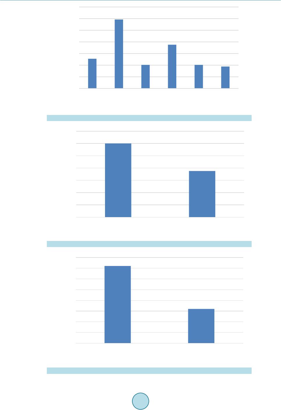 S. Saravanan et al. Figure 15. Comparison of various multipliers based on delay. Figure 1 6. Comparison of reversible multipliers based on delay [27] . Figure 1 7. Comparison of reversible logic unit based on quantum cost [28]. Traditional Array Multiplier Traditional Booth Multiplier Further 2x2 decompose Multiplier Existing Logical Unit [28]  S. Saravanan et al. Table 2. Comparison of conventional multipliers and reversible logic based multipliers. Parameters Conventional Method Reversible Logic Num ber of gat es 88 28 Garbage outputs - 116 4. Conclusion In summary, the proposed reversible multiplier designed using HNG gate used in ALU shows better results in terms of dela y and quantum cost. The proposed reversible logic unit offers better performance in terms of quan- tum cost. Hence the proposed reversible ALU as a whole performs better than the conventional method in terms of quantum cost and delay. In advanced processor architectures there is a dedicated multiplier unit based ALU. In future these irreversible ALU may be replaced with reversible Vedic multiplier based ALU to reduce the quantum cost and delay. Vedic mathematics can be explored to a greater extent to optimize the various VLSI architectures. It is presented above that when these systems are practically realized they require less number of reve rsible gates tha n the conventional method. References [1] Landauer, R. (1961) Irreversibility and Heat Generatio n in the Computing Process. IBM Journal of Research and De- velopment, 5, 183-19 1. http://dx.doi.org/10.1147/rd.53.0183 [2] Bennett, C. (1973) Logical Reversibility of Computation. IBM Journal of Research & Development, 17, 525-532. http://dx.doi.org/10.1147/rd.176.0525 [3] Saravanan, S. and Vennila, I. (2015) Design of Reversible 8 × 8 Vedic Multiplier Using TSG and HNG Gates. Pre- sented in National Conference on Research Issues in Computing Held at PSG College of Technology, Coimbatore. [4] Thapliyal, H. and Ranganathan, N. (2011) A New Design of the Reversible Subtractor Circuit. Proceedings of IEEE International Conference on Nanotechnology, Portland, 15-18 August 2011 1430 -14 35 . [5] Thapliyal, H. and Srinivas, M.B. (2005) A Novel Rever sib le “TS G” Gate and Its Application for Designing Reversible Carry Look-Ahead and Other Adder Architectures. Proceedings of the 10th Asia-Pacific Computer Systems Architec- ture Conference, Springer, Singapore, 805-817 . [6] Haghparast, M., Jassbi, S.J., Navi, K. and Hashemipour, O. (2008) Design of a Novel Reversible Multiplier Circuit Using HNG Gate in Nanotechnology. World Applied Sciences Journal, 3, 974-978. [7] Thapliyal, H. an d Srinivas, M.B. (200 4) High Speed Efficient N X N Bit Parallel Hierarchical Overlay Multiplier Ar- chitecture Based on Ancient Indian Vedic Mathematic. Transactions on Engineering, Computing and Technology, 2, 225-228. [8] Ali Akbar, E.P., Haghparast, M. and Navi, K. (2011) Novel Design o f a Fast Reversib le Wallace Sign Multiplier Cir- cuit in Nanotechnology. Microelectronics Journal, 42, 973-981. http://dx.doi.org/10.1016/j.mejo.2011.05.007 [9] Wille, R. and Groβe, D. (2007) Fast Exact Toffoli Network Synthesis of Reversible Logic. Proceedings of Internation- al Conference on Computer-Aided Design, San Jose, 4-8 Novemb er 2007, 60-64. http://dx.doi.org/10.1109/iccad.2007.4397244 [10] Wille, R., Le, H. M., Du eck, G.W. an d Gr oβe, D. (2008) Quantified Synthesis of R eversible Lo gic. Proceedings of De- sign, Automation & Test in Europe Conference, Munich, 10-14 March 2008, 1015-1020 . [11] Shende, V.V., P rasad, A.K., Markov, I.L. and Hayes, J.P. (2002) Synthesis of Reversible Logic Circuits. Proceedings of International Conference on Computer-Aided Design , San Jose, 10-14 November 2002, 353-360. http://dx.doi.org/10.1109/iccad.2002.1167558 [12] Hung, W.N.N., Song, X., Yang, G., Yang, J. and Perkowski, M. (2004) Quantum Logic Synthesis by Symbolic Rea- chability Analysis. Proceedings of Design Automation Conference, San Diego, 7-11 July 2004, 838-841. [13] Viamontes, G.F., Markov, I.L. and Hayes, J.P. (2007) Checking Equivalence of Quantum Circuits and States. Pro- ceedings of International Conference on CAD, San Jose, 4-8 No vember 2007, 69-74. http://dx.doi.org/10.1109/iccad.2007.4397246 [14] Wang, S.A., Lu, C.Y., Tsai, I.M. and Kuo, S.Y. (2008) An XQDD-Based Verification Method for Quantum Circuits. IEICE Transactions on Fundamentals of Electronics, C om m uni cat ions and Com pute r Sc i e nc e s , E91.A, 584-594. http://dx.doi.org/10.1093/ietfec/e91-a.2.58 4 [15] Wille, R., Gr oße, D., Miller, D.M. and Drech sler, R. (2009 ) Equ ivalence Checki ng of Reversib le Circu its. Internation-  S. Saravanan et al. al Symposium on Multi-Valued Logic, Naha, 21-23 May 2009, 324-330. http://dx.doi.org/10.1109/ismvl.2009.19 [16] Chidgupkar, P.D. and Karad, M.T. (2004) The Implementation of Vedic Algorithms in Digital Signal Processing. Global Journal of Engineering Education, 8, 153-157. [17] Vaid ya, S. and Dandekar, D. (2010) Delay-Power Performance Comparison of Multipliers in VLSI Circuit Design. In- ternational Journal of Computer Networks & Communications (IJCNC), 2, 47-56. http://dx.doi.org/10.5121/ijcnc.2010.2405 [18] Poornima, M., Patil, S.K., Shivukumar, Shridhar, K.P. and Sa njay, H. (2013) Implementation of Multiplier Using Vedic Algorithm. International Journal of Innovative Technology and Exploring Engineering (IJITEE), 2, 219-223. [19] Dhilon, H.S. and Mitra, A. (2 00 8) A Reduced -Bit Multiplication Algorithm for Digital Arithmetic. World Academy of Science, Engineering and Technology, 19, 719-724. [20] Tiwari, H.D., Gan khu yag, G., K i m, C.M. and Cho, Y.B. (2008 ) Multiplier Design Based on Ancien t In di an Ved ic M a- thematics. Proceedings of International Conference on SoC Design, Busan, 24-25 November 2008, 65-68 . [21] Lin , R. (20 04 ) A Reconfigurable Inner Product Processor Architecture Implementing Square Recursive Decomposition of Partial Product Matrices. US Patent No. 6,718,465. [22] Deodhe, Y., Kakde, S. and Deshmukh, R. (2013) Design and Implementation of 8-Bit Vedic Multiplier Using CMOS Logi c. Proceedings of International Conference on Machine Intelligence and Research Advancement (ICMIRA), Kat r a, 21-23 December 2013, 340-344. http://dx.doi.org/10.1109/icmira.2013.71 [23] Kumar, U.C.S.P., Goud, A.S. a nd Radhika, A. (2013) FPGA Implementation of High Speed 8-Bit Vedic Multiplier Using Barrel Shifter. Proceedings of International Conference on Energy Efficient Technologies for Sustainability (ICEETS), Nagercoil, 10-12 April 2013, 14-17. http://dx.doi.org/10.1109/ICEETS.2013.6533349 [24] Haghparast, M. and Sh a ms, M. (2013) A Novel Nanometric Parity Preserving Reversible Vedic Multiplier. Journal of Basic Applied Sciences and Resear ch, 3, 771-776. [25] Saravanan, P., Ch andrasekar, P., Chandran, L., Sriram, N. and Kalpana, P. (2012) Design and Implementation of Effi- cient Vedic Multiplier Using Reversible Logic. In: Rahaman, H., Chattopadhyay, S. and Chattopadhyay, S., Eds., Progress in VLSI Design and Test, Lecture Notes in Computer Sci ence, Vol. 7373, Springer, Berlin, 364-366. http://dx.doi.org/10.1007/978-3-642 -31494 -0_ 45 [26] Viswanath, L. and Ponni, M. (2012 ) Design and Analysis o f 16 Bit Reversi ble ALU. IOSR Journal of Computer Engi- neering (IOSRJCE), 1, 46-53. http://dx.doi.org/10.9790/0661-0114653 [27] Nagarjun, K. and Srinivas, S. (2013) A New Design of Multiplier Using Modified Booth Algorithm and Reversible Gate Lo gi c. International Journal of Computer Applications Technology and Research, 2, 743-747. http://dx.doi.org/10.7753/IJCATR0206.1021 [28] Darshan, H., Mohanraj, R., Kavya, H.B., Monisha, U.K. and Maralabhavi, S. (2015) Design and Synthesis of 8 Bit Reversible Arithmetic & Logical Unit (ALU). Transactions on Electrical and Electronics Engineering (ITSI-TEEE), 3, 2320-2325. [29] Schreiber, M. (2007 ). https://en.wikipedia.org/wiki/Gray_code [30] Landau, S. (2011). http://irreal.org/blog/?p=84 [31] Atmel Corporation (2002). http://www.atmel.com/Images/doc1631.pdf
|