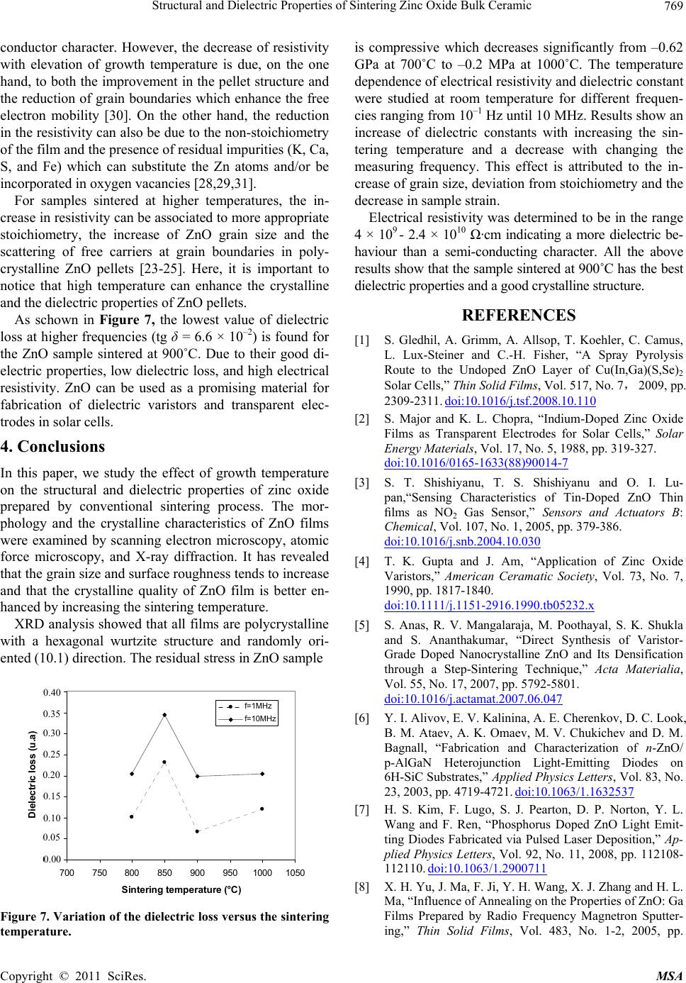
Structural and Dielectric Properties of Sintering Zinc Oxide Bulk Ceramic
Copyright © 2011 SciRes. MSA
770
296-300. doi:10.1016/j.tsf.2005.01.013
[9] J. Hu and R. G. Gordon, “Atmospheric Pressure Chemical
Vapor Deposition of Gallium Doped Zinc Oxide Thin
Films from Diethyl Zinc, Water, and Triethyl Gallium,”
Journal of Applied Physics, Vol. 72, No. 11, 1992, pp.
5381-5392. doi:10.1063/1.351977
[10] K. Y. Cheong, N. Muti and S. R. Ramanan, “Electrical
and optical studies of ZnO: Ga Thin Films Fabricated via
the Sol-gel Technique,” Thin Solid Film, Vol. 410, No.
1-2, 2002, pp. 142-146.
doi:10.1016/S0040-6090(02)00286-9
[11] A. Zaier, F. Oum Elaz, F. Lakfif, A. Kabir, S. Boudjadar
and M. S. Aida, “A Novel Synthesis of Nanostructured
ZnO via Thermal Oxidation of Zn Nanowires Obtained by
a Green Route,” Metirial Science in Semiconductor Proc-
essing, Vol. 12 ,2009, pp. 279-284.
[12] J. Nause and B. Nemeth, “Pressurized Melt Growth of
ZnO Boules,” Semiconductor Science and Technology,
Vol. 20, No. 4, 2005, p. S45.
doi:10.1088/0268-1242/20/4/005
[13] K. Jacobs, D. Schulz, D. Klimm and S. Ganschow, “Melt
Growth of ZnO Bulk Crystals in Ir Crucibles,” Solid State
Sciences, Vol. 12, No. 3, 2010, pp. 307-310.
doi:10.1016/j.solidstatesciences.2009.05.015
[14] Y. Caglar, S. Aksoy, S. Ilican and M. Cagmar, “Crystal-
line Structure and Morphological Properties of Undoped
and Sn Doped ZnO Thin Films,” Superlattices and Mi-
crostructures, Vol. 46, 2009, pp. 469-475.
doi:10.1016/j.spmi.2009.05.005
[15] B. D. Cullity and S. R. Stock, “Elements of X-ray Dif-
fraction,” 3rd Edition, Prentice Hall, Upper Saddle River,
2001.
[16] F. Hamdani, A. Botchkarev, W. Kim, H. Morkoç, M.
Yeadon, J. M. Gibson, S.-C. Y. Tsen, David J. Smith, D.
C. Reynolds, D. C. Look, K. Evans, C. W. Litton, W. C.
Mitchel and P. Hemenger, “Optical Properties of GaN
Grown on ZnO by Reactive Molecular Beam Epitaxy,”
Applied Physics Letters, Vol. 70, No. 4, 1997, pp. 467-
469. doi:10.1063/1.118183
[17] A. Umar, S. H. Kim, Y. B. Hahn, “Sea-Urchin Like ZnO
Nanostructures on Si by Oxidation of Zn Metal Powders:
Structural and Optical Properties,” Superlattices and Mi-
crostructures, Vol. 39, No. 1-4, 2006, pp. 145-152.
doi:10.1016/j.spmi.2005.08.067
[18] N. Wang, J. Li, H. R. Peng and G. C. Li, “Synthesis of
ZnO Nanostructures Composed of Nanosheets with Con-
trollable Morphologies,” Crystal Research Technology,
Vol. 44, No. 3, 2009, pp. 341-345.
doi:10.1002/crat.200800445
[19] L. Kumari and W. Z. Li, “Synthesis, Structure and Optical
Properties of Zinc Oxide Hexagonal Microprisms,” Crys-
tal Research Technology, Vol. 45, No. 3, 2010, pp. 311-
315. doi:10.1002/crat.200900600
[20] E. M. Bachari, G. Baud, S. B. Amor and M. Jacquet,
“Structural and Optical Properties of Sputtered ZnO
Films,” Thin Solid Films, Vol. 348, No. 1-2, 1999, pp.
165-172. doi:10.1016/S0040-6090(99)00060-7
[21] T. V. Vimalkumar, N. Poornima, C. S. Kartha and K. P.
Vijayakumar, “On Tuning the Orientation of Grains of
Spray Pyrolysed ZnO Thin Films,” Applied Surface Sci-
ence, Vol. 256, No. 20, 2010, pp. 6025-6028.
doi:10.1016/j.apsusc.2010.03.113
[22] M. Matsuoka and K. Ono, “Photochromism and Anoma-
lous Crystallite Orientation of ZnO Films Prepared by a
Sputtering—Type Electron Cyclotron Resonance Micro-
wave Plasma,” Applied Physics Letters, Vol. 53, No. 15,
1988, pp. 1393-1395. doi:10.1063/1.99987
[23] T. P. Rao, M. C. S. Kumar, A. Safarullaa, V. Ganesan, S.
R. Barman and C. Sanjeeviraja, “Physical Properties of
ZnO Thin films Deposited at Various Substrate Tempera-
tures Using Spray Pyrolysis,” Physica B: Condensed
Matter, Vol. 405, No. 9, 2010, pp. 2226-2231.
doi:10.1016/j.physb.2010.02.016
[24] M. K.Puchet, P. Y. Timbrell and R. N. Lamb, “Post
Deposition Annealing of Radio Frequency Magnetron
Sputtered ZnO Films,” Journal of Vacuum Science &
Technology A, Vol. 14, No. 4, 1996, pp. 2220-2230.
doi:10.1116/1.580050
[25] T. P. Rao and M. C. S. Kumar, “Effect of Thickness on
Structural, Optical and Electrical Properties of Nanos-
tructured ZnO Thin films by Spray Pyrolysis,” Applied
Surface Science, Vol. 255, No. 8, 2009, pp. 4579-4584.
doi:10.1016/j.apsusc.2008.11.079
[26] H. Li, J. Wang, H. Liu, H. Zhang and X. Li, “Zinc Oxide
Films Prepared by Sol-Gel Method,” Journal of Crystal
Growth, Vol. 275, No. 1-2, 2005, pp. 943-946.
doi:10.1016/j.jcrysgro.2004.11.098
[27] J. W. Zhai, L. Y. Zhang and X. Yao, “The Dielectric
Properties and Optical Propagation Loss of c-axis Ori-
ented ZnO Thin Films Deposited by Sol-gel Process,”
Ceramics International, Vol. 26, No. 8. 2000, pp. 883-885.
doi:10.1016/S0272-8842(00)00031-6
[28] H. Gomez, A. Maldonado, M. de la L. Olvera and D. R.
Acosta, “Gallium-Doped ZnO Thin Films Deposited by
Chemical Spray,” Solar Energy Materials & Solar Cells,
Vol. 87, No. 1-4, 2005, pp. 107-116.
doi:10.1016/j.solmat.2004.07.016
[29] M. de la L. Olvera, A. Maldonado, R. Asomoza and M.
Meléndez-Lira, “Effect of the Substrate Temperature and
Acidity of the Spray Solution on the Physical Properties
of F-Doped ZnO Thin Films Deposited by Chemical
Spray,” Solar Energy Materials & Solar Cells, Vol. 71,
No. 1, 2002, pp. 61-71.
doi:10.1016/S0927-0248(01)00044-7
[30] A. Zaier, F. Oum El az, F. Lakfif, A. Kabir, S. Boudjadar
and M. S. Aida, “Effects of the Substrate Temperature and
Solution Molarity on the Structural Opto-Electric Proper-
ties of ZnO Thin Films Deposited by Spray Pyrolysis,”
Materials Science in Semiconductor Processing, Vol. 12,
No. 6, 2009, pp. 207-211. doi:10.1016/j.mssp.2009.12.002
[31] C. H. Pandis, N. Brilis, D. Tsamakis, H. A. Ali, S. Krish-
namoorthy and A. A. Iliadis, “Role of Low O2 Pressure
and Growth Temperature on Electrical Transport of PLD
Grown ZnO Thin films on Si Substrates,” Solid-State
Electronics, Vol. 50, No. 6, 2006, pp. 1119-1123.
doi:10.1016/j.sse.2006.04.025