Paper Menu >>
Journal Menu >>
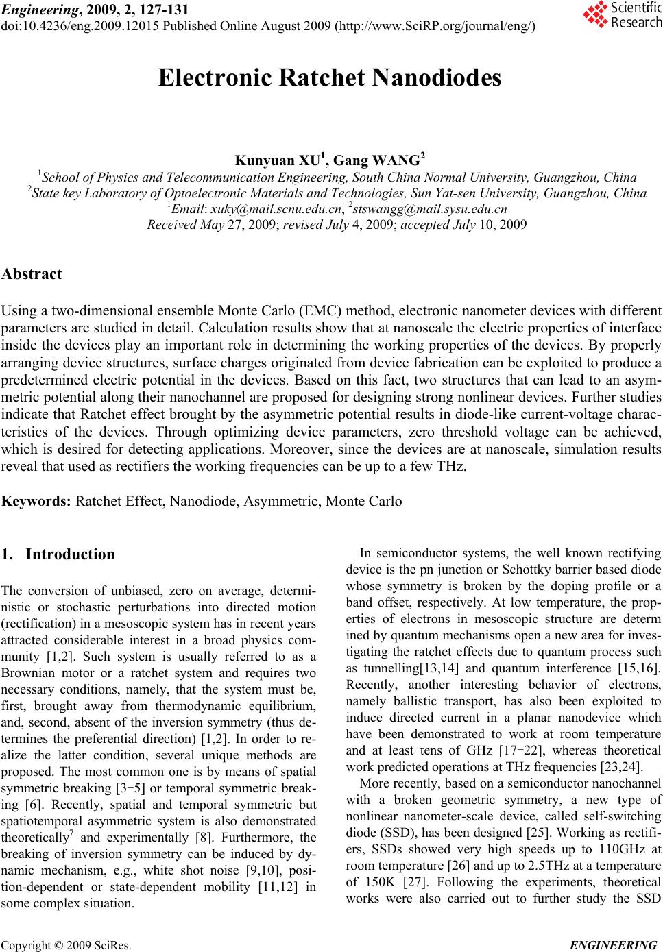 Engineering, 2009, 2, 127-131 doi:10.4236/eng.2009.12015 Published Online August 2009 (http://www.SciRP.org/journal/eng/) Copyright © 2009 SciRes. ENGINEERING Electronic Ratchet Nanodiodes Kunyuan XU1, Gang WANG2 1School of Physics and Telecommunication Engineering, South China Normal University, Guangzhou, China 2State key Laboratory of Optoelectronic Materials and Technologies, Sun Yat-sen University, Guangzhou, China 1Email: xuky@mail.scnu.edu.cn, 2stswangg@mail.sysu.edu.cn Received May 27, 2009; revised July 4, 2009; accepted July 10, 2009 Abstract Using a two-dimensional ensemble Monte Carlo (EMC) method, electronic nanometer devices with different parameters are studied in detail. Calculation results show that at nanoscale the electric properties of interface inside the devices play an important role in determining the working properties of the devices. By properly arranging device structures, surface charges originated from device fabrication can be exploited to produce a predetermined electric potential in the devices. Based on this fact, two structures that can lead to an asym- metric potential along their nanochannel are proposed for designing strong nonlinear devices. Further studies indicate that Ratchet effect brought by the asymmetric potential results in diode-like current-voltage charac- teristics of the devices. Through optimizing device parameters, zero threshold voltage can be achieved, which is desired for detecting applications. Moreover, since the devices are at nanoscale, simulation results reveal that used as rectifiers the working frequencies can be up to a few THz. Keywords: Ratchet Effect, Nanodiode, Asymmetric, Monte Carlo 1. Introduction The conversion of unbiased, zero on average, determi- nistic or stochastic perturbations into directed motion (rectification) in a mesoscopic system has in recent years attracted considerable interest in a broad physics com- munity [1,2]. Such system is usually referred to as a Brownian motor or a ratchet system and requires two necessary conditions, namely, that the system must be, first, brought away from thermodynamic equilibrium, and, second, absent of the inversion symmetry (thus de- termines the preferential direction) [1,2]. In order to re- alize the latter condition, several unique methods are proposed. The most common one is by means of spatial symmetric breaking [3-5] or temporal symmetric break- ing [6]. Recently, spatial and temporal symmetric but spatiotemporal asymmetric system is also demonstrated theoretically7 and experimentally [8]. Furthermore, the breaking of inversion symmetry can be induced by dy- namic mechanism, e.g., white shot noise [9,10], posi- tion-dependent or state-dependent mobility [11,12] in some complex situation. In semiconductor systems, the well known rectifying device is the pn junction or Schottky barrier based diode whose symmetry is broken by the doping profile or a band offset, respectively. At low temperature, the prop- erties of electrons in mesoscopic structure are determ ined by quantum mechanisms open a new area for inves- tigating the ratchet effects due to quantum process such as tunnelling[13,14] and quantum interference [15,16]. Recently, another interesting behavior of electrons, namely ballistic transport, has also been exploited to induce directed current in a planar nanodevice which have been demonstrated to work at room temperature and at least tens of GHz [17-22], whereas theoretical work predicted operations at THz frequencies [23,24]. More recently, based on a semiconductor nanochannel with a broken geometric symmetry, a new type of nonlinear nanometer-scale device, called self-switching diode (SSD), has been designed [25]. Working as rectifi- ers, SSDs showed very high speeds up to 110GHz at room temperature [26] and up to 2.5THz at a temperature of 150K [27]. Following the experiments, theoretical works were also carried out to further study the SSD 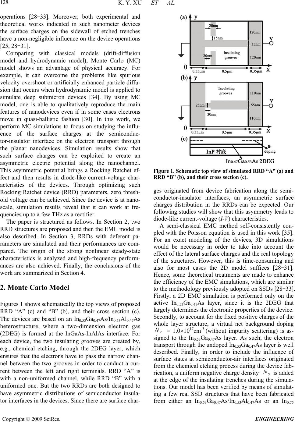 K. Y. XU ET AL. 128 operations [28-33]. Moreover, both experimental and theoretical works indicated in such nanometer devices the surface charges on the sidewall of etched trenches have a non-negligible influence on the device operations [25, 28-31]. Comparing with classical models (drift-diffusion model and hydrodynamic model), Monte Carlo (MC) model shows an advantage of physical accuracy. For example, it can overcome the problems like spurious velocity overshoot or artificially enhanced particle diffu- sion that occurs when hydrodynamic model is applied to simulate deep submicron devices [34]. By using MC model, one is able to qualitatively reproduce the main features of nanodevices even if in some cases electrons move in quasi-ballistic fashion [30]. In this work, we perform MC simulations to focus on studying the influ- ence of the surface charges at the semiconduc- tor-insulator interface on the electron transport through the planar nanodevices. Simulation results show that such surface charges can be exploited to create an asymmetric electric potential along the nanochannel. This asymmetric potential brings a Rocking Ratchet ef- fect and then results in diode-like current-voltage char- acteristics of the devices. Through optimizing such Rocking Ratchet device (RRD) parameters, zero thresh- old voltage can be achieved. Since the device is at nano- scale, simulation results reveal that it can work at fre- quencies up to a few THz as a rectifier. The paper is structured as follows. In Section 2, two RRD structures are proposed and then the EMC model is also described. In Section 3, RRDs with deferent pa- rameters are simulated and their performances are com- pared. The origin of the strong nonlinear steady-state characteristics is analyzed and high-frequency perform- ances are also achieved. Finally, the conclusions of the work are summarized in Section 4. 2. Monte Carlo Model Figures 1 shows schematically the top views of proposed RRD “A” (c) and “B” (b), and their cross section (c). The devices are based on an In0.53Ga0.47As/In0.53Al0.47As heterostructure, where a two-dimension electron gas (2DEG) is formed at the InGaAs-InAlAs interface. For each device, the two insulating grooves are created by, e.g., chemical etching, through the 2DEG layer, which ensures that the electrons have to pass the narrow chan- nel between the two grooves in order to conduct a cur- rent between the left and right terminals. RRD “A” is with a non-uniformed channel, while RRD “B” with a uniformed one. But the two RRDs are both designed to have asymmetric distributions of semiconductor insula- tor interfaces in the devices. Since there are surface char- Figure 1. Schematic top view of simulated RRD “A” (a) and RRD “B” (b), and their cross section (c). ges originated from device fabrication along the semi- conductor-insulator interfaces, an asymmetric surface charges distribution in the RRDs can be expected. Our following studies will show that this asymmetry leads to diode-like current-voltage (I-V) characteristics. A semi-classical EMC method self-consistently cou- pled with the Poisson equation is used in this work [35]. For an exact modeling of the devices, 3D simulations would be necessary in order to take into account the effect of the lateral surface charges and the real topology of the structures. However, this is time-consuming and also for most cases the 2D model suffices [28-31]. Hence, some theoretical treatments are made to enhance the efficiency of the EMC simulations, which are similar to the methodology previously adopted on SSDs [28-33]. Firstly, a 2D EMC simulation is performed only on the active In0.53Ga0.47As layer, since it is the 2DEG that largely determines the electronic properties of the device. Secondly, to account for the fixed positive charges of the whole layer structure, a virtual net background doping V N = 1.01017cm-3 (without impurity scattering) is as- signed to the In0.53Ga0.47As layer. As such, the electron transport through the undoped In0.53Ga0.47As layer is well described. Finally, in order to include the influence of surface states at semiconductor-air interfaces originated from the chemical etching process during the device fab- rication, a uniform negative charge density S N is added at the edge of the insulating trenches during the simula- tions. Our model has been verified by means of simulat- ing a few real SSD structures that have been fabricated from either an In0.53Ga0.47As/In0.53Al0.47As or an In0.75 C opyright © 2009 SciRes. ENGINEERING  K. Y. XU ET AL. Copyright © 2009 SciRes. ENGINEERING 129 Ga0.25As/InP devices and a good agreement was obtained between the simulated and measured I-V characteristics [36]. 3. Results and Discussion In this section, efforts are devoted to a deep study of RRDs, including the origin of diode-like I-V characteristics, the effect of surface charge density on the steady-state performance, and the rectification properties. During EMC simulations, the left terminal of the devices is grounded and a sweeping voltage from -1.6V to 1.6V with a step of 0.2V is added on the right terminal of the devices as shown in Figure 1(a) & (b). At each applied voltage, the simulation has been carried out for a long enough time to ensure that the devices reach a steady state. Simulation results of the steady-state I-V character- Figure 2. Current-voltage characteristics of RRD “A” and “B” showing diode-like characteristics. Figure 3. Electric potential variation along the center of the nanochannel at applied biases of V = 0.4 V, 0.2 V and 0 V. istics of the two proposed RRDs (“A” and “B”) with a negative surface charge density S N =-0.151012cm-2, are plotted in Figure 2. It can be found that for applied voltages with the same absolute value, current induced by a negative one is always larger than that by a positive one, showing asymmetric electron transport in the de- vices. As we mentioned in Section I, asymmetric transport is always relative to the absent of some inversion symmtry. Here the surface charge profile and the device geometry are both with broken symmetry. The asymmetric geome try of RRD “A” is because of the two isolated areas which unlike that of SSDs can not block the transport of electrons. Meanwhile, RRD “B” is just like two con- nected resistors. Based on the two facts, one can easily expect that the asymmetric geometry of considered RRDs makes little contribution to the asymmetric transport. Figure 4 I-V characteristics of RRD “B” with surface charge densities of Ns=-0.15×10¹²/cm2 (1), -0.20×10¹²/cm2 (2), -0.25×10¹²/cm2 (3) and -0.27×10¹²/cm2 (4). Figure 5 Frequency responses of RRD “B” with virtually zero threshold voltage, showing gradual reduce of the DC current with the frequency.  K. Y. XU ET AL. 130 In order to investigate the effect of surface charge asymmetry, the electric potential variation along the center of the devices (also the center of the nanochannel) is calculated and the results of RRD “A” at different ap- plied biases of V = 0.4 V, 0.2 V and 0 V are shown in Figure 3. Since the negative charge will produce an elec- tric field to prevent the approaching of electrons, an asymmetric electric potential barrier emerges along the nanochannel even at zero bias. The absent of this electric potential barrier will block the electrons and make it dif- ferent for them to flow through the nanochannel. By ap- plying a voltage on the right terminal of the device, one can lower this electric potential barrier so that making the electrons pass through the nanochannel easier. As shown in Figure 3, the electric potential barrier responds to not only the amplitude but also the sign of applied voltage. Obviously, a negative voltage has more effi- ciency on lowering the electric potential barrier than a positive one, which is called as Rocking Ratchet Effect [1,2]. This effect leads to a strong asymmetric electron transport through the devices resulting in diode-like I-V characteristics as shown in Figure 2. To further investigate the effect of surface charges on the device performances, RRDs with various surface charge densities are simulated. The results of RRD “B” with surface charge densities of Ns=-0.15×10¹²/cm2, -0.20×10¹²/cm2, -0.25×10¹²/cm2 and -0.27×10¹²/cm2 are shown in Figure 4. One can find that with the increase of surface charge density the current reduces while the ratio of negative current to positive one increases. The incre- ment of this current ratio indicates a growing of asym- metric transport through the device which followed re- sults in an enhancement of nonlinear I-V characteristics near zero bias. By choosing a proper surface charge den- sity N s between -0.25~0.27×10¹²/cm2, a virtually zero threshold voltage of the device can be obtained as shown in Figure 4. Virtually zero threshold voltage is desired in practical applications for not only simplifying the addi- tional circuit but also reducing the 1/f noise [37]. Al- though the surface charge density is difficult to exactly control during device fabrications, one can alternatively change the width of nanochannel to obtain a virtually zero threshold voltage. With strong nonlinearity at zero bias, RRDs are ex- pected to use as a high-speed rectifier to convert micro- wave signal to dc signal. To confirm this, a sinusoidal signal with amplitude of 0.25 V is applied to the right terminal while the left terminal is grounded. The recti- fied current is then calculated at frequencies from 100 GHz to several THz. Figure 5 shows the simulation re- sults for the RRD “B” with virtually zero threshold volt- age. Although with the increase of signal frequency, the dc output reduced gradually, the device has non-zero dc output at frequency up to 3 THz, showing a potential for THz applications. 4. Conclusions A 2D ensemble Monte Carlo simulation has been carried out to study the electric properties of RRDs, including the origin of diode-like I-V characteristics, the effect of surface charge density on the steady-state performance, and the rectification properties. Simulation results show that at nanoscale the surface charges originated from device fabrication have a strong influence on the electric potential in the device and can be exploited to produce a predetermined asymmetric electric potential barrier along the nanochannel by properly arranging the inner etched insulating grooves of the devices. Based on this asymmetric potential barrier, two RRDs with diode-like I-V characteristics are proposed and their working prin- ciple is explained in terms of Rocking Ratchet effect. Since the proposed devices possess strong nonlinear I-V characteristics, they may be useful in composing planar integrated circuits. Moreover, the above strong nonlinear feature exists even in the case of very high frequency (up to 3 THz) showing strong potential applications, such as power detectors or multipliers, in THz region. 5. Acknowledgements This work is supported by “Xiangshi” Fund of School of Physics and Telecommunication Engineering, South China Normal University, Guangzhou, China. 6. References [1] P. Reimann, “Brownian motors: Noisy transport far from equilibrium,” Physical Report, Vol. 361, pp. 57-265, 2002. [2] P. Hänggi, Fabio Marchesoni, and Franco Nori, “Brownian motors,” Annal of Physics (Leipzig), Vol. 14, pp. 51-70, 2005. [3] J. Prost, J. F. Chauwin, L. Peliti, and A. Ajdari, “Asym- metric pumping of particles,” Physical Review Letters, Vol. 72, pp. 2652-2655, 1994. [4] R. D. Astumian and M. Bier, “Fluctuation driven ratchets: Molecular motors,” Physical Review Letters, Vol. 72, pp. 1766-1769, 1994. [5] C. R. Doering, W. Horsthemke, and J. Riordan, “Non- equilibrium fluctuation-induced transport,” Physical Re- view Letters, Vol. 72, pp. 2984-2987, 1994. [6] M. I. Dykman, H. Rabitz, V. N. Smelyanskiy, and B. E. Vugmeister, “Resonant directed diffusion in nonadia- batically driven systems,” Physical Review Letters, Vol. 79, pp. 1178-1181, 1997. [7] L. Sanchez-Palencia, “Resonant directed diffusion in nonadiabatically driven systems,” Physical Review E, Vol. 70, pp. 011102-1~4, 2004. [8] P. Sjölund, S. H. H. Petra, C. M. Dion, S. Jonsell, M. Nylén, L. Sanchez-Palencia, and A. Kastberg, “Resonant C opyright © 2009 SciRes. ENGINEERING  K. Y. XU ET AL. Copyright © 2009 SciRes. ENGINEERING 131 directed diffusion in nonadiabatically driven systems,” Physical Review Letters, Vol. 96, pp. 190602-1~4, 2006. [9] P. Hänggi, R. Bartussek, P. Talkner, and J. Łuczka, “Noise-induced transport in symmetric periodic poten- tials: While shot noise versus deterministic noise,” Euro- physical Letters, Vol. 35, pp. 315-317, 1996. [10] T. Czernik and J. Łuczka, “Rectified steady flow induced by white shot noise: Diffusive and non-diffusive re- gimes,” Annal Physics (Leipzig), Vol. 9, pp. 721-734, 2000. [11] R. H. Luchsinger, “Transport in nonequilibrium systems with position-dependent mobility,” Physical Review E, Vol. 62, 272-275, 2000. [12] D. Dan, M. C. Mahato, and A. M. Jayannavar, “Motion in a rocked ratchet with spatially periodic friction,” Physical A, Vol. 296, 375-390, 2001. [13] P. Reimann, M. Grifoni, and P. Hänggi, “Quantum ratch- ets,” Physical Review Letters, Vol. 79, pp. 10-13, 1997. [14] H. Linke, T. E. Humphrey, A. Löfgren, A. O. Sushkov, R. Newbury, R. P. Taylor, and P. Omling, “Experimental tunneling ratchets,” Science, Vol. 286, 2314-2317, 1999. [15] H. Linke, W. D. Sheng, A. Löfgren, H. Q. Xu, P. Omling, and P. E. Lindelof, “A quantum dot ratchet: Experiment and theory,” Europhysical Letters, Vol. 44, pp. 341-347, 1998. [16] H. Linke, W. D. Sheng, A. Svensson, A. Löfgren, L. Christensson, H. Q. Xu, P. Omling, and P. E. Lindelof, “Asymmetric nonlinear conductance of quantum dots with broken inversion symmetry,” Physical Review B, Vol. 61, pp. 15914-15926, 2000. [17] A. M. Song, P. Omling, L. Samuelson, W. Seifert, I. Shorubalko, and H. Zirath, “Operation of In- GaAs/InP-based ballistic rectifiers at room-temperature and frequencies up to 50 GHz,” Japanese Journal of Ap- plied Physics, Part 2, Vol. 40, pp. L909-L911, 2001. [18] A. M. Song, P. Omling, L. Samuelson, W. Seifert, I. Shorubalko, and H. Zirath, “Room-temperature and 50 GHz operation of a functional nanomaterial,” Applied Physical Letters, Vol. 79, pp. 1357-1359, 2001. [19] I. Shorubalko, H. Q. Xu, and I. Maximov, “Nonlinear operation of GaInAs/InP-based three-terminal ballistic junctions,” Applied Physical Letters, Vol. 79, pp. 1384-1386, 2001. [20] I. Shorubalko, H. Q. Xu, I. Maximov, D. Nilsson, P. Omling, L. Samuelson, and W. Seifert, “A novel fre- quency-multiplication device based on three-terminal ballistic junction,” IEEE Electron Device Letters, Vol. 23, pp. 377-379, 2002. [21] L. Worschech, B. Weidner, S. Reitzenstein, and A. For- chel, “Investigation of switching effects between the drains of an electron Y-branch switch,” Applied Physical Letters, Vol. 78, pp. 3325-3327, 2001. [22] L. Worschech, H. Q. Xu, A. Forchel, and L. Samuelson, “Bias-voltage-induced asymmetry in nanoelectronic Y-branches,” Applied Physical Letters, Vol. 79, pp. 3287-3289, 2001. [23] J. Mateos, B. G. Vasallo, D. Pardo, T. González, J. S. Galloo, Y. Roelens, S. Bollaert and A. Cappy, Nano- technology 14, Vol. 117, 2003. [24] B. G. Vasallo, T. González, D. Pardo, and J. Mateos, “Monte carlo analysis of four-terminal ballistic rectifi- ers,” Nanotechnology, Vol. 15, pp. S250-S253, 2004. [25] A. M. Song, M. Missous, P. Omling, A. R. Peaker, L. Samuelson, and W. Seifert, “Unidirectional electron flow in a nanometer-scale semiconductor channel: A self- switching device,” Applied Physical Letters, Vol. 83, pp. 1881-1883, 2003. [26] C. Balocco, A. M. Song, M. Åberg, A. Forchel, T. Gon- zález, J. Mateos, I. Maximov, M. Missous, A. A. Rezazadeh, J. Saijets, L. Samuelson, D. Wallin, K. Wil- liams, L. Worschech, and H. Q. Xu, “Microwave detec- tion at 110 GHz by naonwires with broken symmetry,” Nano Letters, Vol. 5, pp. 1423-1427, 2005. [27] C. Balocco, M. Halsall, N. Q. Vinh, and A. M. Song, “THz operation of asymmetric-nanochannel devices,” Journal Physical Condensed Matter, Vol. 20, pp. 384203-1~5, 2008. [28] J. Mateos, B. G. Vasallo, D. Pardo, and T. González, “Operation and high-frequency performance of nanoscale unipolar rectifying diodes,” Applied Physical Letters, Vol. 86, pp. 212103-1~3, 2005. [29] I. Iñiguez–de-la-Torre, J. Mateos, D. Pardo, and T. Gon- zález, “Monte Carlo analysis of noise spectra in self-switching nanodiodes,” Jounal of Applied Physics, Vol. 103, 024502-1~6, 2008. [30] J. Mateos, A. M. Song, B. G. Vasallo1, D. Pardo1, and T. González1, “THz operation of self-switching nano-de- vices and nano-transistors,” Proceedings of SPIE, Vol. 5838, pp. 145-153, 2005. [31] I. Iñiguez–de-la-Torre, J. Mateos, D. Pardo, A. M. Song, and T. González, “Noise and terahertz rectification linked by geometry in planar asymmetric nanodiodes,” Applied Physical Letters, Vol. 94, pp. 093512-1~3, 2009. [32] K. Y. Xu, X. F. Lu, G. Wang, and A. M. Song, “En- hanced terahertz detection by localized surface plasma oscillations in a nanoscale unipolar diode,” Jounal of Ap- plied Physical Letters, Vol. 103, pp. 113708-1~8, 2008. [33] K. Y. Xu, X. F. Lu, A. M. Song, and G. Wang, “Tera- hertz harmonic generation using a planar nanoscale uni- polar diode at zero bias,” Applied Physical Letters, Vol. 92, 163503-1~3, 2008. [34] C. Jungemann and B. Meinerzhagen, “Hierarchical de- vice simulation: The monte-carlo perspective,” Springer, New York, 2003. [35] C. Jacoboni and P. Lugli, “The monte carlo method for semiconductor device simulation,” Springer, New York, 1989. [36] K. Y. Xu, X. F. Lu, G. Wang, and A. M. Song, “Strong spatial dependence of electron velocity, density, and in- ter-valley scattering in an asymmetric nanodevice in the nonlinear transport regime”, IEEE Transactions on Nanotechnology, Vol. 7, pp. 451, 2008. [37] S. -Y. Park, R. Yu, S. -Y. Chung, P. R. Berger, P. E. Thompson, and P. Fay, “Sensitivity of Si-based zero-bias backward diodes for microwave detection,” IEEE Elec- tronical Letters, Vol. 43, pp. 53-54, 2007. |