 Engineering, 2009, 2, 111-116 doi:10.4236/eng.2009.12013 Published Online August 2009 (http://www.SciRP.org/journal/eng/). Copyright © 2009 SciRes. ENGINEERING Fabrication of Si-PDMS Low Voltage Capillary Electrophoresis Chip Wenwen GU1,2,3,4, Zhiyu WEN1,2,3,4, Zhongquan WEN1,2,3,4, Yi XU1,2,3, Fengfei LIANG1,2,3, Xiaoguo HU1,2,3 1Key Laboratory of Fundamental Science of Micro/Nano-Device and System Technology, Chongqing, China 2National Center for International Research of Micro/Nano-System and New Material Technology, Chongqing, China 3Microsystem Research Center, Chongqing University, Chongqing, China 4College of Optoelectronic Engineering, Chongqing University, Chongqing, China Received May 11, 2009; revised July 2, 2009; accepted July 10, 2009 ABSTRACT This paper discusses the fabrication of Si-PDMS low voltage capillary electrophoresis chip (CE chip). Ar- rayed-electrode which is used to apply low separation voltage is fabricated along the sidewalls of the separa- tion channel on the silicon based bottom part. Isolation trenches, which are placed surrounding the ar- rayed-electrode, insure the insulation between the arrayed-electrode, as well as arrayed-electrode and liquid in the micro channel. Polydimethylsilicone (PDMS) is used as the cover. PDMS and silicon based bottom part are reversible sealed to attain Si-PDMS low voltage CE chip. Experiments have been done to obtain op- timum electrophoresis separation condition: separation voltage is 45V, switch time is 2s and the Phe and Lys electrophoresis separation is successful. Keywords: Low Voltage, Arrayed-Electrode, Si-PDMS, CE Chip 1. Introduction Lab on a Chip, or called Miniaturized Total Analysis System (µ-TAS [1]), which has features of miniature, fast, high performance and throughput, has become a hot research topic in analytical chemistry. Capillary Elec- trophoresis Chip (CE chip) is a highly integrated minia- ture separation and analysis device within the develop- ment of biotechnology and MEMS (Micro-Electro-Mechanic Systems) technology. It can integrate sample treatment, injection, separation and detector into a microchip which is only several square centimeters. In CE chip, micro channels form network, and controlled microfluidic runs through all the system [2]. With the development of CE chip and widely applications, many fields such as disease diagnosis, environmentent monitoring, new drug devel- opment, food safety inspection will be changed thor- oughly. Nowadays, it has already become one of the most important study subjects in chemistry, life science, MEMS, physics, micro-electronics and etc [3,4]. Taking a wide view of the related research status [5-8], working voltage which is from several hundreds to thou- sands is directly applied in the two ends of the separation channel of the CE chip. There are some shortages bought by high voltage, such as huge equipments, high thermal effect and high safety protection requirements for labo- ratory operators. High voltage also restricts the minia- turization, home application and portability for CE chip. According to the moving gradient electrical field the- ory of CE chip, the separation channel can be equivalent to series connections of several shorter ones. Using ar- rayed-electrode to apply low separation voltage section by section can obtain the demanded high separation elec- tric field. So the difficult problem brought by CE chip requiring high separation voltage has been overcome [9-12]. Based on the idea above, a new approach has been proposed to fabricate low voltage CE chip. Silicon-on- insulator (SOI) wafer is used as the substrate material of the silicon based bottom part, where there is a cross channel and arrayed-electrode. Arrayed-electrode and isolation trenches are fabricated along the micro channel 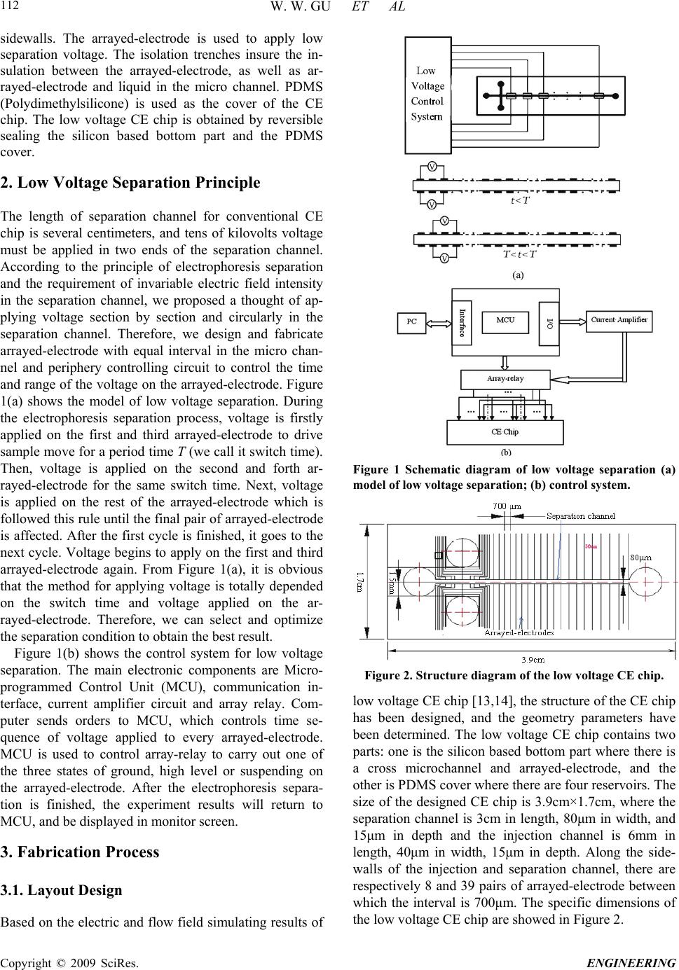 W. W. GU ET AL Copyright © 2009 SciRes. ENGINEERING 112 sidewalls. The arrayed-electrode is used to apply low separation voltage. The isolation trenches insure the in- sulation between the arrayed-electrode, as well as ar- rayed-electrode and liquid in the micro channel. PDMS (Polydimethylsilicone) is used as the cover of the CE chip. The low voltage CE chip is obtained by reversible sealing the silicon based bottom part and the PDMS cover. 2. Low Voltage Separation Principle The length of separation channel for conventional CE chip is several centimeters, and tens of kilovolts voltage must be applied in two ends of the separation channel. According to the principle of electrophoresis separation and the requirement of invariable electric field intensity in the separation channel, we proposed a thought of ap- plying voltage section by section and circularly in the separation channel. Therefore, we design and fabricate arrayed-electrode with equal interval in the micro chan- nel and periphery controlling circuit to control the time and range of the voltage on the arrayed-electrode. Figure 1(a) shows the model of low voltage separation. During the electrophoresis separation process, voltage is firstly applied on the first and third arrayed-electrode to drive sample move for a period time T (we call it switch time). Then, voltage is applied on the second and forth ar- rayed-electrode for the same switch time. Next, voltage is applied on the rest of the arrayed-electrode which is followed this rule until the final pair of arrayed-electrode is affected. After the first cycle is finished, it goes to the next cycle. Voltage begins to apply on the first and third arrayed-electrode again. From Figure 1(a), it is obvious that the method for applying voltage is totally depended on the switch time and voltage applied on the ar- rayed-electrode. Therefore, we can select and optimize the separation condition to obtain the best result. Figure 1(b) shows the control system for low voltage separation. The main electronic components are Micro- programmed Control Unit (MCU), communication in- terface, current amplifier circuit and array relay. Com- puter sends orders to MCU, which controls time se- quence of voltage applied to every arrayed-electrode. MCU is used to control array-relay to carry out one of the three states of ground, high level or suspending on the arrayed-electrode. After the electrophoresis separa- tion is finished, the experiment results will return to MCU, and be displayed in monitor screen. 3. Fabrication Process 3.1. Layout Design Based on the electric and flow field simulating results of Figure 1 Schematic diagram of low voltage separation (a) model of low voltage separation; (b) control system. Figure 2. Structure diagram of the low voltage CE chip. low voltage CE chip [13,14], the structure of the CE chip has been designed, and the geometry parameters have been determined. The low voltage CE chip contains two parts: one is the silicon based bottom part where there is a cross microchannel and arrayed-electrode, and the other is PDMS cover where there are four reservoirs. The size of the designed CE chip is 3.9cm×1.7cm, where the separation channel is 3cm in length, 80μm in width, and 15μm in depth and the injection channel is 6mm in length, 40μm in width, 15μm in depth. Along the side- walls of the injection and separation channel, there are respectively 8 and 39 pairs of arrayed-electrode between which the interval is 700μm. The specific dimensions of the low voltage CE chip are showed in Figure 2. 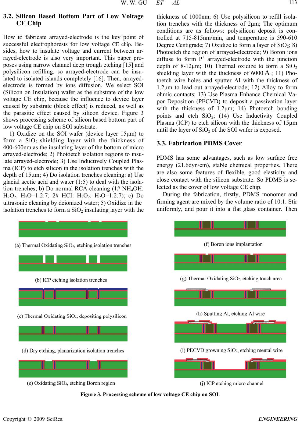 W. W. GU ET AL Copyright © 2009 SciRes. ENGINEERING 113 3.2. Silicon Based Bottom Part of Low Voltage CE Chip How to fabricate arrayed-electrode is the key point of successful electrophoresis for low voltage CE chip. Be- sides, how to insulate voltage and current between ar- rayed-electrode is also very important. This paper pro- poses using narrow channel deep trough etching [15] and polysilicon refilling, so arrayed-electrode can be insu- lated to isolated islands completely [16]. Then, arrayed- electrode is formed by ions diffusion. We select SOI (Silicon on Insulation) wafer as the substrate of the low voltage CE chip, because the influence to device layer caused by substrate (block effect) is reduced, as well as the parasitic effect caused by silicon device. Figure 3 shows processing scheme of silicon based bottom part of low voltage CE chip on SOI substrate. 1) Oxidize on the SOI wafer (device layer 15μm) to form a SiO2 shielding layer with the thickness of 400-600nm as the insulating layer of the bottom of micro arrayed-electrode; 2) Photoetch isolation regions to insu- late arrayed-electrode; 3) Use Inductively Coupled Plas- ma (ICP) to etch silicon in the isolation trenches with the depth of 15μm; 4) Do isolation trenches cleaning: a) Use glacial acetic acid and water (1:5) to deal with the isola- tion trenches; b) Do normal RCA cleaning (1# NH4OH: H2O2: H2O=1:2:7; 2# HCI: H2O2: H2O=1:2:7); c) Do ultrasonic cleaning by deionized water; 5) Oxidize in the isolation trenches to form a SiO2 insulating layer with the thickness of 1000nm; 6) Use polysilicon to refill isola- tion trenches with the thickness of 2μm; The optimum conditions are as follows: polysilicon deposit is con- trolled at 715-815nm/min, and temperature is 590-610 Degree Centigrade; 7) Oxidize to form a layer of SiO2; 8) Photoetch the region of arrayed-electrode; 9) Boron ions diffuse to form P+ arrayed-electrode with the junction depth of 8-12μm; 10) Thermal oxidize to form a SiO2 shielding layer with the thickness of 6000 ; 11) Pho- toetch wire holes and sputter Al with the thickness of 1.2μm to lead out arrayed-electrode; 12) Alloy to form ohmic contacts; 13) Use Plasma Enhance Chemical Va- por Deposition (PECVD) to deposit a passivation layer with the thickness of 1.2μm; 14) Photoetch bonding points and etch SiO2; (14) Use Inductivity Coupled Plasma (ICP) to etch silicon with the thickness of 15μm until the layer of SiO2 of the SOI wafer is exposed. 3.3. Fabrication PDMS Cover PDMS has some advantages, such as low surface free energy (21.6dyn/cm), stable chemical properties. There are also some features of flexible, good elasticity and close contact with the silicon substrate. So PDMS is se- lected as the cover of low voltage CE chip. During the fabrication, firstly, PDMS monomer and firming agent are mixed by the volume ratio of 10:1. Stir uniformly, and pour it into a flat glass container. Then Figure 3. Processing scheme of low voltage CE chip on SOI. 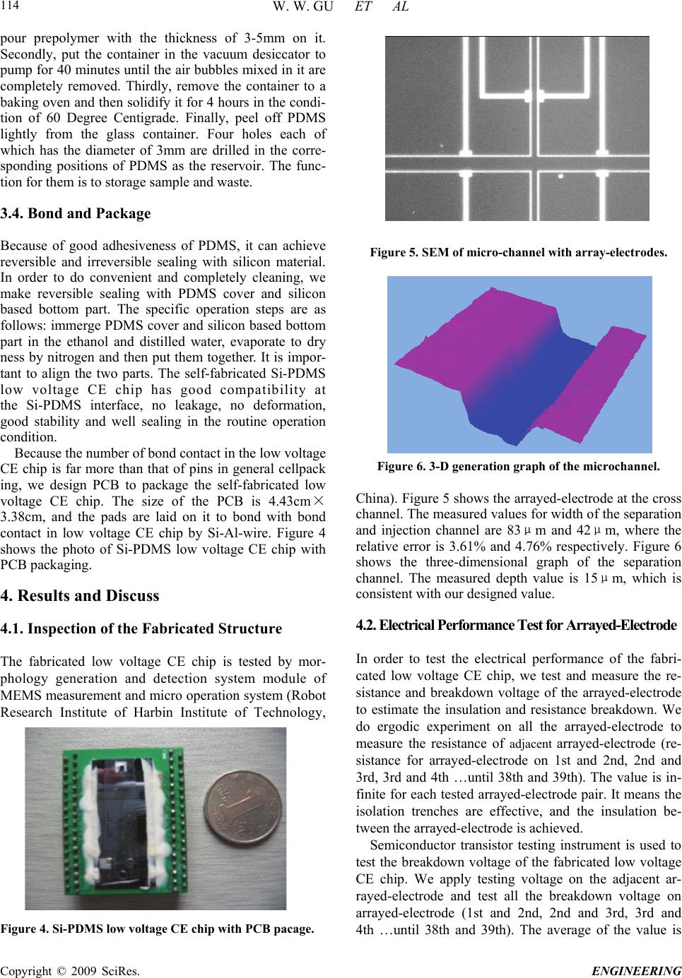 W. W. GU ET AL Copyright © 2009 SciRes. ENGINEERING 114 pour prepolymer with the thickness of 3-5mm on it. Secondly, put the container in the vacuum desiccator to pump for 40 minutes until the air bubbles mixed in it are completely removed. Thirdly, remove the container to a baking oven and then solidify it for 4 hours in the condi- tion of 60 Degree Centigrade. Finally, peel off PDMS lightly from the glass container. Four holes each of which has the diameter of 3mm are drilled in the corre- sponding positions of PDMS as the reservoir. The func- tion for them is to storage sample and waste. 3.4. Bond and Package Because of good adhesiveness of PDMS, it can achieve reversible and irreversible sealing with silicon material. In order to do convenient and completely cleaning, we make reversible sealing with PDMS cover and silicon based bottom part. The specific operation steps are as follows: immerge PDMS cover and silicon based bottom part in the ethanol and distilled water, evaporate to dry ness by nitrogen and then put them together. It is impor- tant to align the two parts. The self-fabricated Si-PDMS low voltage CE chip has good compatibility at the Si-PDMS interface, no leakage, no deformation, good stability and well sealing in the routine operation condition. Because the number of bond contact in the low voltage CE chip is far more than that of pins in general cellpack ing, we design PCB to package the self-fabricated low voltage CE chip. The size of the PCB is 4.43cm× 3.38cm, and the pads are laid on it to bond with bond contact in low voltage CE chip by Si-Al-wire. Figure 4 shows the photo of Si-PDMS low voltage CE chip with PCB packaging. 4. Results and Discuss 4.1. Inspection of the Fabricated Structure The fabricated low voltage CE chip is tested by mor- phology generation and detection system module of MEMS measurement and micro operation system (Robot Research Institute of Harbin Institute of Technology, Figure 4. Si-PDMS low voltage CE chip with PCB pacage. Figure 5. SEM of micro-channel with array-electrodes. Figure 6. 3-D generation graph of the microchannel. China). Figure 5 shows the arrayed-electrode at the cross channel. The measured values for width of the separation and injection channel are 83μm and 42μm, where the relative error is 3.61% and 4.76% respectively. Figure 6 shows the three-dimensional graph of the separation channel. The measured depth value is 15μm, which is consistent with our designed value. 4.2. Electrical Performance Test for Arrayed-Electrode In order to test the electrical performance of the fabri- cated low voltage CE chip, we test and measure the re- sistance and breakdown voltage of the arrayed-electrode to estimate the insulation and resistance breakdown. We do ergodic experiment on all the arrayed-electrode to measure the resistance of adjacent arrayed-electrode (re- sistance for arrayed-electrode on 1st and 2nd, 2nd and 3rd, 3rd and 4th …until 38th and 39th). The value is in- finite for each tested arrayed-electrode pair. It means the isolation trenches are effective, and the insulation be- tween the arrayed-electrode is achieved. Semiconductor transistor testing instrument is used to test the breakdown voltage of the fabricated low voltage CE chip. We apply testing voltage on the adjacent ar- rayed-electrode and test all the breakdown voltage on arrayed-electrode (1st and 2nd, 2nd and 3rd, 3rd and 4th …until 38th and 39th). The average of the value is 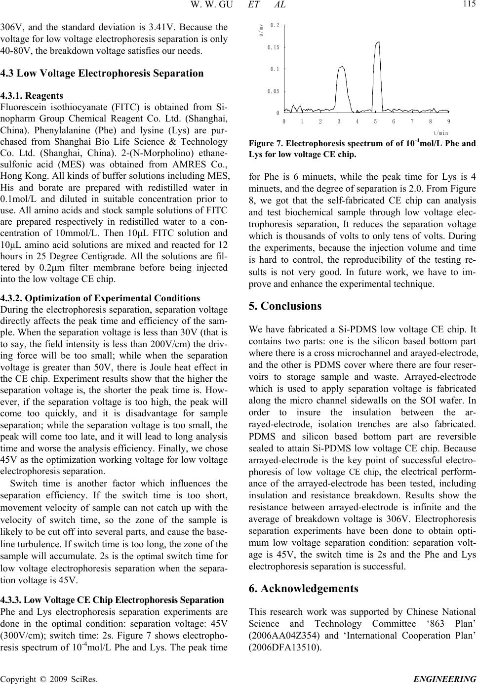 W. W. GU ET AL Copyright © 2009 SciRes. ENGINEERING 115 0 0.05 0.1 0.15 0.2 0123456789 t/min u/mv 306V, and the standard deviation is 3.41V. Because the voltage for low voltage electrophoresis separation is only 40-80V, the breakdown voltage satisfies our needs. 4.3 Low Voltage Electrophoresis Separation 4.3.1. Reagents Fluorescein isothiocyanate (FITC) is obtained from Si- nopharm Group Chemical Reagent Co. Ltd. (Shanghai, China). Phenylalanine (Phe) and lysine (Lys) are pur- chased from Shanghai Bio Life Science & Technology Co. Ltd. (Shanghai, China). 2-(N-Morpholino) ethane- sulfonic acid (MES) was obtained from AMRES Co., Hong Kong. All kinds of buffer solutions including MES, His and borate are prepared with redistilled water in 0.1mol/L and diluted in suitable concentration prior to use. All amino acids and stock sample solutions of FITC are prepared respectively in redistilled water to a con- centration of 10mmol/L. Then 10μL FITC solution and 10μL amino acid solutions are mixed and reacted for 12 hours in 25 Degree Centigrade. All the solutions are fil- tered by 0.2μm filter membrane before being injected into the low voltage CE chip. 4.3.2. Optimization of Experimental Conditions During the electrophoresis separation, separation voltage directly affects the peak time and efficiency of the sam- ple. When the separation voltage is less than 30V (that is to say, the field intensity is less than 200V/cm) the driv- ing force will be too small; while when the separation voltage is greater than 50V, there is Joule heat effect in the CE chip. Experiment results show that the higher the separation voltage is, the shorter the peak time is. How- ever, if the separation voltage is too high, the peak will come too quickly, and it is disadvantage for sample separation; while the separation voltage is too small, the peak will come too late, and it will lead to long analysis time and worse the analysis efficiency. Finally, we chose 45V as the optimization working voltage for low voltage electrophoresis separation. Switch time is another factor which influences the separation efficiency. If the switch time is too short, movement velocity of sample can not catch up with the velocity of switch time, so the zone of the sample is likely to be cut off into several parts, and cause the base- line turbulence. If switch time is too long, the zone of the sample will accumulate. 2s is the optimal switch time for low voltage electrophoresis separation when the separa- tion voltage is 45V. 4.3.3. Low Voltage CE Chip Electrophoresis Separation Phe and Lys electrophoresis separation experiments are done in the optimal condition: separation voltage: 45V (300V/cm); switch time: 2s. Figure 7 shows electropho- resis spectrum of 10-4mol/L Phe and Lys. The peak time Figure 7. Electrophoresis spectrum of of 10-4mol/L Phe and Lys for low voltage CE chip. for Phe is 6 minuets, while the peak time for Lys is 4 minuets, and the degree of separation is 2.0. From Figure 8, we got that the self-fabricated CE chip can analysis and test biochemical sample through low voltage elec- trophoresis separation, It reduces the separation voltage which is thousands of volts to only tens of volts. During the experiments, because the injection volume and time is hard to control, the reproducibility of the testing re- sults is not very good. In future work, we have to im- prove and enhance the experimental technique. 5. Conclusions We have fabricated a Si-PDMS low voltage CE chip. It contains two parts: one is the silicon based bottom part where there is a cross microchannel and arayed-electrode, and the other is PDMS cover where there are four reser- voirs to storage sample and waste. Arrayed-electrode which is used to apply separation voltage is fabricated along the micro channel sidewalls on the SOI wafer. In order to insure the insulation between the ar- rayed-electrode, isolation trenches are also fabricated. PDMS and silicon based bottom part are reversible sealed to attain Si-PDMS low voltage CE chip. Because arrayed-electrode is the key point of successful electro- phoresis of low voltage CE chip, the electrical perform- ance of the arrayed-electrode has been tested, including insulation and resistance breakdown. Results show the resistance between arrayed-electrode is infinite and the average of breakdown voltage is 306V. Electrophoresis separation experiments have been done to obtain opti- mum low voltage separation condition: separation volt- age is 45V, the switch time is 2s and the Phe and Lys electrophoresis separation is successful. 6. Acknowledgements This research work was supported by Chinese National Science and Technology Committee ‘863 Plan’ (2006AA04Z354) and ‘International Cooperation Plan’ (2006DFA13510).  W. W. GU ET AL Copyright © 2009 SciRes. ENGINEERING 116 7. References [1] A. Manz, N. Graber, and H. M. Widmer, “Miniaturized total chemical analysis systems: A novel concept for chemical sensing,” Sensors and Actuators B, Vol. 7, pp. 244-248, 1990. [2] N. A. Lacher, K. E. Garrison, and R. S. Martin, “Micro- chip capillary electrophoresis/electro-chemistry,” Elec- trophoresis, Vol. 22, pp. 2526-2536, 2001. [3] Y. Jin, G. A. Luo, and R. J. Wang, “Development of in- tegrated capillary electrophoresis chips,” Chinese Journal of Chromatography, Vol. 4, pp. 313-317, 2000. [4] C. Koppmu and A. D. Manz, “Development in technol- ogy and application of microsystems,” Current Opinion in Chemical Biology, Vol. 1, pp. 410-419, 1997. [5] J. C. Fister, S. C. Jacobson, and J. M. Ramsey, “Ultrasen- sitive crosscorrelation electrophoresis on microchip de- vices, Analytical Chemistry, Vol. 71, pp. 4460-4464, 1999. [6] J. Qian, Y. Wu, H. Yang, A. C. Michael, “An integrated decoupler for capillary electrophoresis with electrochemi- cal detection: Application to analysis of brain microdialy- sate,” Analytical Chemistry, Vol. 71, pp. 4486-4492, 1999. [7] Y. Shi, P. C. Simpon, J. R. Scherer, and D. Wexler, “Ra- dial capillary array electrophoresis microplate and scan- ner for high-performance nucleic acid analysis,” Analyti- cal Chemistry, Vol. 71, pp. 5354-5361, 1999. [8] J. Wang, M. P. Chatrathi, B. Tian, and R. Polsky, “Micro- fabricated electrophoresis chips for simultaneous bioas- says of glucose, uric acid, ascorbic acid, and acetamino- phen,” Analytical Chemistry, Vol. 72, pp. 2514-2518, 2000. [9] Y. C. Lin and W. D. Wu, “Arrayed-electrode design for moving electric field driven capillary electrophoresis chips,” Sensors and Actuators B, Vol. 73, pp. 54-62, 2001. [10] L. M. Fu and R. J. Yang, “Low-voltage driven control in electrophoresis microchips by traveling electric field,” Electrophoresis, Vol. 24, pp. 1253-1260, 2003. [11] X. Li, Z. Y. Wen, and H. X. Li, “Low voltage separation model and its control system for electrophoresis chip,” Micronanoelectronic Technology, Vol. 7/8, pp. 344-346, 2003. [12] Y. Wu, Z. Y. Wen, and Z. P. Jiang, “Low voltage separa- tion model and discussion for electrophoresis chip,” Opto-Electronic Engineering, Vol. 29, pp. 27-33, 2002. [13] Z. Y. Wen, Y. Xu, and X. Li, “Electric field simulation of separation mode on low voltage electrophoresis chip,” Optoelectronic Engineering, Vol. 9, pp. 35-41, 2006. [14] Y. Xu, Z. Y. Wen, and X. Li, “Fluidic field simulation of separation mode on low voltage electrophoresis chip by ConventerWare,” Chinese Journal of Sensors and Actua- tors, Vol. 8, pp. 1070-1075, 2007. [15] Z. Y. Zhang, S. L. Xu, and Y. K. Liu, “A Study on silicon deep etching technology,” Microelectronics, Vol. 2, pp. 519-521, 2004. [16] Y. Wu, Y. Q. Jiang, and Z. Y. Wen, “Development of polycrystalline silicon micro-electrode array on silicon substrate,” Semiconductor Optoelectronics, Vol. 4, pp. 317-319, 2005.
|