Ef fect of Annealing on Structural, Morphological, Electrical and Optical Studies of Nickel Oxide Thin Fil ms
Copyright © 2011 SciRes. JSEMAT
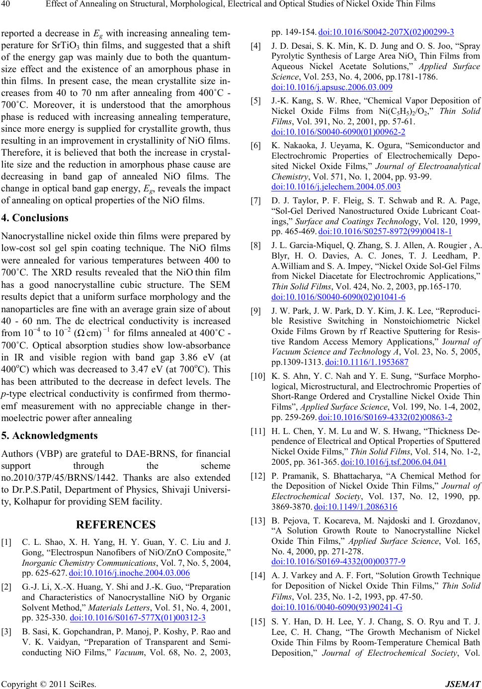
reported a decrease in Eg with increasing annealing tem-
perature for SrTiO3 thin films, and suggested that a shift
of the energy gap was mainly due to both the quantum-
size effect and the existence of an amorphous phase in
thin films. In present case, the mean crystallite size in-
creases from 40 to 70 nm after annealing from 400˚C -
700˚C. Moreover, it is understood that the amorphous
phase is reduced with increasing annealing temperature,
since more energ y is supplied for cr ystallite growth, thus
resul ti n g i n an i mpr o ve me nt i n crysta llinit y o f N iO fi l ms .
Therefore, it is believed that both the increase in crystal-
lite size and the reduction in amorphous phase cause are
decreasing in band gap of annealed NiO films. The
change in optical band gap energy, Eg, reveals the impact
of annealing on optical properties of the NiO films.
4. Conclusions
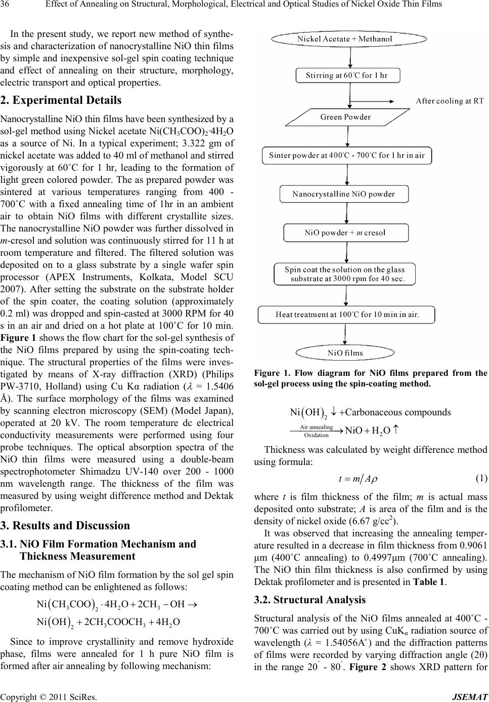
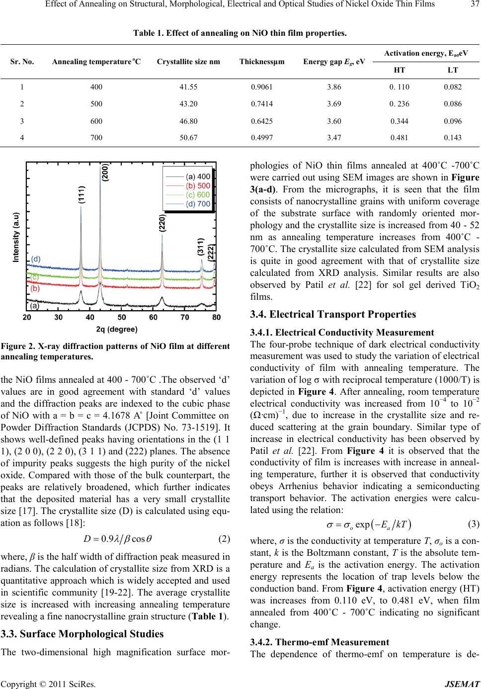
Nanocrystalline nickel oxide thin films were prepared by
low-cost sol gel spin coating technique. The NiO films
were annealed for various temperatures between 400 to
700˚C. The XRD results revealed that the NiO thin film
has a good nanocrystalline cubic structure. The SEM
results depict that a uniform surface morphology and the
nanopar ticles are fine with an average grain size of about
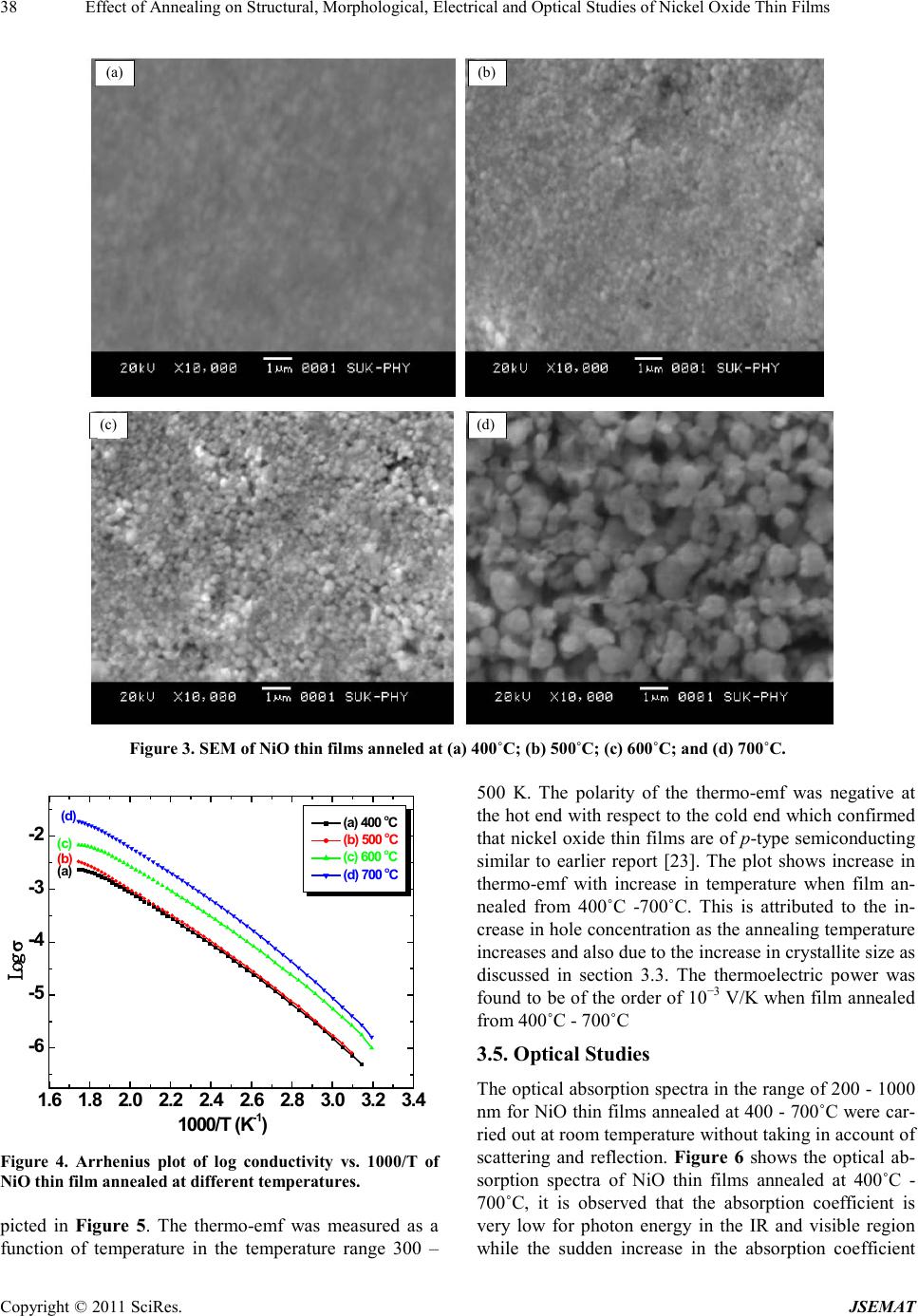
40 - 60 nm. The dc electrical conductivity is increased
fro m 10−4 to 10−2 (Ω·cm) −1 for films annealed at 400˚C -
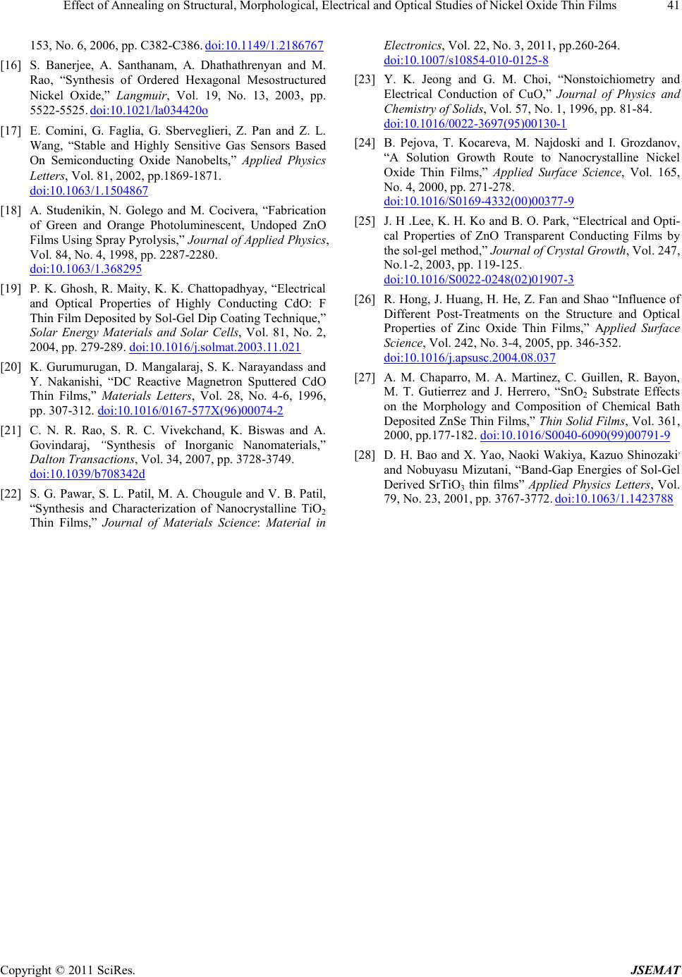
700˚C. Optical absorption studies show low-absorbance
in IR and visible region with band gap 3.86 eV (at
400oC) which was decreased to 3.47 eV (at 700oC). T his
has been attributed to the decrease in defect levels. The
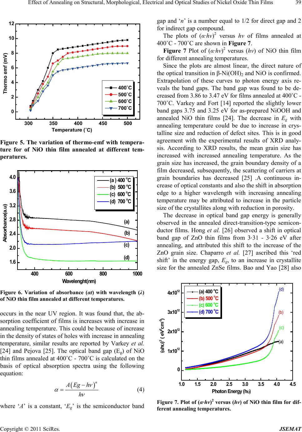
p-type electrical conductivity is confirmed from thermo-
emf measurement with no appreciable change in ther-
moelectric power after a nnealing
5. Acknowledgments
Authors (VBP) are grateful to DAE-BRNS, for financial
support through the scheme
no.2010/37P/45/BRNS/1442. Thanks are also extended
to Dr.P.S.Patil, Department of Physics, Shivaji Universi-
ty, Kolhapur fo r providi ng S EM fa cility.
REFERENCES
[1] C. L. Shao, X. H. Yang, H. Y. Guan, Y. C. Liu and J.
Gong, “Electrospun Nanofibers of NiO/ZnO Composite,”
Inorganic Chemistry Communications, Vol. 7, No. 5, 2004,
pp. 625-627. doi:10.1016/j.inoche.2004.03.006
[2] G.-J. Li , X .-X. Huang, Y. Shi and J.-K. Guo, “Preparation
and Charact er istics of Nanocrystalline NiO by Organic
Solvent Method,” Materials Letters, Vol. 51 , No . 4, 2001,
pp. 325-330. doi:10.1016/S0167-577X(01)00312-3
[3] B. Sasi, K. Gopchandran, P. Manoj, P. Koshy, P. Rao and
V. K. Vaidyan, “Preparation of Transparent and Semi-
conducting NiO Films,” Vacuum, Vol. 68, No. 2, 2003,
pp. 149-154. doi:10.1016/S0042-207X(02)00299-3
[4] J. D. Desai, S. K. Min, K. D. Ju ng and O. S. Joo, “Spray
Pyrolytic Synthesis of Large Area NiOx Thin Films from
Aqueous Nickel Acetate Solutions,” Applied Surface
Scien ce, Vol. 253, No. 4, 2006, pp.1781-1786.
doi:10.1016/j.apsusc.2006.03.009
[5] J.-K. Kang, S. W. Rhee, “Chemical Vapor Deposition of
Nickel Oxide Films from Ni(C5H5)2/O2,” Thin Solid
Films, Vol. 391, No. 2, 20 01 , pp. 57-61.
doi:10.1016/S0040-6090(01)00962-2
[6] K. Nakaoka, J. Ueyama, K. Ogura, “Semiconductor and
Electrochromic Properties of Electrochemically Depo-
sited Nickel Oxide Films,” Journal of Electroanalytical
Chemistry, Vol. 571, No. 1, 2004, pp. 93-99.
doi:10.1016/j.jelechem.2004.05.003
[7] D. J. Taylor, P. F. Fleig, S. T. Schwab and R. A. Page,
“Sol-Ge l Derived Nanostructured Oxide Lubricant Coat-
ings,” Surface and Coatings Technol ogy, Vol. 120, 1999,
pp. 465-469. doi:10.1016/S0257-8972(99)00418-1
[8] J. L. Garcia-Miquel, Q. Zhang, S. J. Allen, A. Rougier , A.
Blyr, H. O. Davies, A. C. Jones, T. J. Leedham, P.
A.William and S. A. Impey, “Nickel Oxide Sol-Gel Films
from Nickel Diacetate for Electrochromic Applications,”
Thin Solid Films, Vol. 424, No. 2, 2003, pp.165-170.
doi:10.1016/S0040-6090(02)01041-6
[9] J. W. Park, J. W. Park, D. Y. Kim, J. K. Lee, “Repr od uci-
ble Resistive Switching in Nonstoichiometric Nickel
Oxide Films Grown by rf Reactive Sputtering for Resis-
tive Random Access Memory Applications,” Journal of
Vacuum Science and Technology A, V ol. 23, No . 5, 2005,
pp.1309-1313. doi:10.1116/1.1953687
[10] K. S. Ahn, Y. C. Nah and Y. E. Sung, “Su rface Morpho-
logical, Micro structu ral, and E lectrochr omic Prop erties of
Short-Range Ordered and Crystalline Nickel Oxide Thin
Films”, Applied Surface S cience, Vol. 199, No. 1 -4, 2002,
pp. 259-269. doi:10.1016/S0169-4332(02)00863-2
[11] H. L. Chen, Y. M. Lu and W. S. Hwang, “Thicknes s De-
pendence of Electri cal and Optical Properties of Spu ttered
Nickel Oxide Films,” Thin Solid Films, Vol. 514, No. 1-2,
2005, p p. 361 -365. doi:10.1016/j.tsf.2006.04.041
[12] P. Pramanik, S. Bhattacharya, “A Chemical Method for
the Deposition of Nickel Oxide Thin Films,” Journal of
Electrochemical Society, Vol. 137, No. 12, 1990, pp.
3869-3870. doi:10.1149/1.2086316
[13] B. Pejova, T. Kocareva, M. Najdoski and I. Grozdanov,
“A Solution Growth Route to Nanocrystalline Nickel
Oxide Thin Films,” Applied Surface Scien ce, Vol. 165,
No. 4, 2000, pp. 271-278.
doi:10.1016/S0169-4332(00)00377-9
[14] A. J. V arke y and A. F. Fort, “Solution Growth Technique
for Deposition of Nickel Oxide Thin Films,” Thin Solid
Films, Vol. 235, No. 1-2, 1993, pp. 47-50.
doi:10.1016/0040-6090(93)90241-G
[15] S. Y. Han, D. H. Lee, Y. J. Chang, S. O. Ryu and T. J.
Lee, C. H. Chang, “The Growth Mechanism of Nickel
Oxide Thin Films by Room-Temperature Chemical Bath
Deposition,” Journal of Electrochem ical Society, Vol.