Journal of Electromagnetic Analysis and Applications
Vol.07 No.03(2015), Article ID:54993,10 pages
10.4236/jemaa.2015.73011
Design of Integrated Triple Band Notched for Ultra-Wide Band Microstrip Antenna
Yahya S. H. Khraisat, Ahmad Bataineh, Malak Angor
Electrical and Electronics Department, Al-Balqa’ Applied University/Al-Huson University College, Irbid, Jordan
Email: Yahya_khr@bau.edu.jo, a_bataineh75@bau.edu.jo, dr.angormalak@bau.edu.jo
Copyright © 2015 by authors and Scientific Research Publishing Inc.
This work is licensed under the Creative Commons Attribution International License (CC BY).
http://creativecommons.org/licenses/by/4.0/


Received 28 January 2015; accepted 22 March 2015; published 25 March 2015
ABSTRACT
Ultra-wideband (UWB) is one of the recent topics that received a great concern from academia and industry. However, UWB found many difficulties to be standardized due to the overlay working that made UWB an important potential interference source to many licensed and unlicensed spectrum throughout the band 3.1 to 10.6 GHz. This paper demonstrates the design of integrated triple band notched for UWB Microstrip antenna. We simulated UWB short range systems which require low power and these are built using inexpensive digital components. We proposed a compact triple band notched CPW (Co-planar Waveguide) fed Micro strip Antenna (MSA) for UWB. This band-notched antenna has rejection characteristics at 3.2 GHz (for Wi-MAX band 3.16 to 3.32 GHz), at 5.5 GHz (for WLAN 2 band―5.3 to 5.72 GHz) and at 7.9 GHz (for ITU band 7.72 GHz to 8.13 GHz). The simulation was done using IE3D simulator.
Keywords:
Ultra Wide Band Antenna, Microstrip Antenna, Partial Ground Plane, Band-Notched

1. Introduction
In 2002, the Federal Communications Commission (FCC) allocated the ultra-wideband (UWB) frequency range from 3.1 - 10.6 GHz for unlicensed UWB applications. The limitation of equivalent isotropically radiated power (EIRP) in band emission does not exceed −41.3 dBm/MHz for extremely wide impedance bandwidth [1] . Printed planar monopole antennas have been designed to operate in UWB systems [2] . There are some wireless communication applications which have already occupied frequencies in the UWB band such as the wireless local area network (WLAN) a.k.a. IEEE 802.11 a/g and HIPERLAN/2 WLAN which operate at 5.15 - 5.35 GHz and 5.725 - 5.825 GHz, respectively and IEEE 802.16 (3.3 - 3.8 GHz) [3] . In addition, the worldwide interoperability for microwave access (WiMAX) has also operated covering the frequency from 5.25 - 5.85 GHz in some countries [4] . One way to suppress these interfering signals is to use a spatial filter such as a frequency selective surface above the antenna. However, this approach requires too much space and is expensive [5] . To disband this problem, the UWB antenna with build-in frequency notch structure is often chosen. A lot of functions have been used for frequency rejection in UWB antenna designs. The most popular technique to provide this character is embedded a slot on the patch or ground plane [6] . However, in order to achieve monopole antenna designing, a large ground plane is required, which could not be suitable for compact wireless devices. Some techniques are used to reject undesired frequencies, for examples, placing the parasitic strips on the opposite side of the radiating element [7] , inserting two strips in the printed slot antenna to create two rejection bands [8] , and embedding a C-shaped slit into the fed element with a parasitic strip in slot antenna [9] . However, the antennas have more complicated structures to implement than others. In [10] , the band-notched slot antennas were studied, in which two types of narrow slits on the exciting stubs were used for two antennas, and two parasitic strips were placed in the rectangular slot for another one [11] . Although, the antenna design is capable of undesired frequency rejection, the parasitic strips lead to more complex structure.
2. Antenna Design
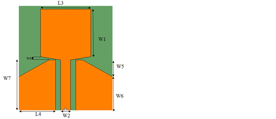
First a Primitive antenna is taken. This antenna consists of a beveled rectangular radiating patch and a CPW (co- planar waveguide) type feed structure Figure 1. The essence of this design strategy is that three notching elements are embedded onto the primitive patch antenna to produce band-stop filtering function at those above mentioned frequencies. Notch elements are meticulously selected and embedded onto the antenna [12] .
The band notches are introduced in order to stop the function of the antenna in that particular frequency range. By this the interference between the UWB system and the narrow band system is reduced to a great extent. Introduction of the band notches helps us to avoid the use of the band stop filters and hence reducing the cost and complexity of the antenna. Now-a-days demand is for miniaturized technology and MSA helps us in achieving that.
2.1. Primitive Antenna
Antenna Description
Measurements of the primitive antenna are shown in Table 1.
Primitive antenna consists of a rectangular patch (trimmed) and trimmed ground plane to enhance the antenna’s broadband performance and also this arrangement increases the flow of surface current through the feed- line and concentrates the surface current around the bottom of the radiating patch. First a rectangular patch is designed using simulation program IE3D and then it is trimmed by removing triangular shaped parts using the extrude feature. Triangular shaped parts are also removed from the rectangular shaped ground plane in order to smooth the surface current flow. Radiating patch is made using PEC (Perfect Electrical Conductor) material.
Figure 1. Geometry of CPW fed planar antenna.
・ Dielectric material used here has relative permittivity = 4.4.
・ Thickness of substrate = 1.6 mm.
・ Length of substrate = 28 mm.
・ Width of substrate = 31 mm.
・ Tangent Loss = 0.003 [8] .
2.2. Antenna with C-Slot (for Band-Notch at 3.2 GHz)
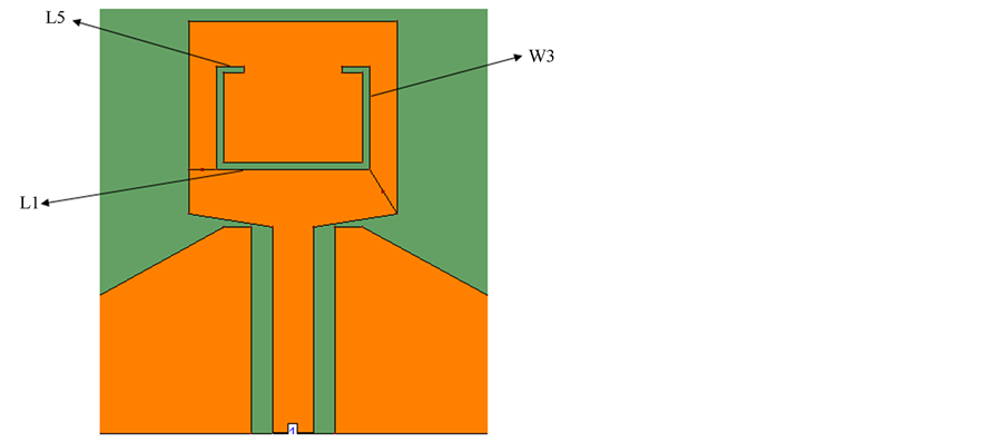
Figure 2 shows the antenna design with C?slot to produce band?notched at 3.2 GHz.
Antenna Description:
Measurements of the C-shaped slot at 3.5GHz is shown in Table 2.
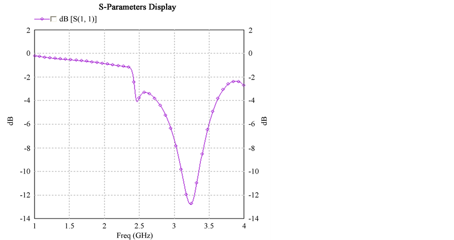
FCC (Federal Communication Commission) approved and authorized the 3.1 GHz to 10.6 GHz band as the UWB. But Wi-MAX operates in the range of 3.16 GHz to 3.32 GHz and interferes with UWB devices. So instead of using a band-stop filter at the receiver antenna we have etched a C-shaped slot on the radiating patch in order to facilitate band-rejection facility around 3.2 GHz, so that the interference is minimized. The S?para- meters of this design is shown in Figure 3.
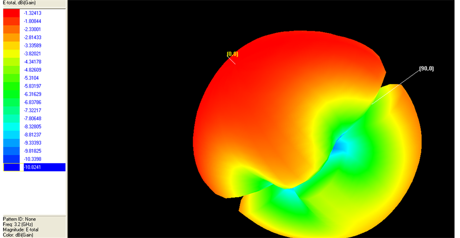
The 3-D radiation pattern is shown in Figure 4.
2.3. Antenna with C-Slot (for Band-Notch at 5.5 GHz)
Table 1. Measurements of the primitive antenna (without any slots).
Figure 2. Geometry of antenna with C-slot to produce band-notch at 3.2 GHz.
Table 2. Measurements of the C-shaped slot (band notch at 3.5 GHz).
Figure 3. Band-notch at 3.2 GHz return loss.
Figure 4. 3D radiation pattern for 3.2GHz with max gain 3.28.
Antenna Description:
Measurements of the C-shaped slot at 5.5 GHz is shown below in Table 3.
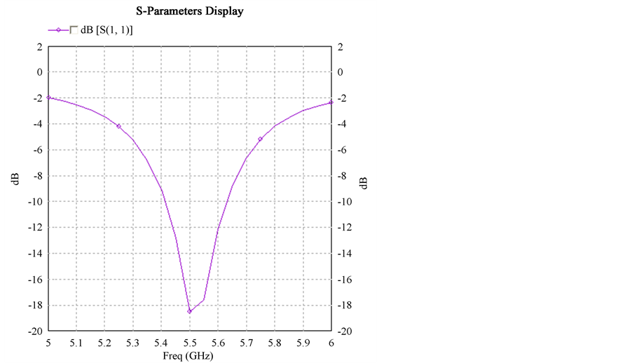
WLAN 2 operates from 5.3 GHz to 5.72 GHz, interferes with the UWB systems. In order to minimize the interference we have etched a C-shaped slot on the radiating patch to create a notch around 5.5 GHz.
The S-parameters of this design is shown in Figure 6.
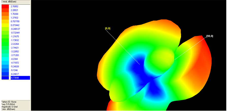
The 3-D radiation pattern is shown in Figure 7.
2.4. Antenna with Two CSRRs
Antenna Description:
Measurements of the two CSRRs at 7.9 GHz is shown in Table 4.
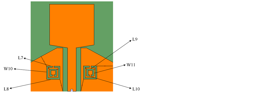
ITU band operates in the range of 7.72 GHz to 8.13 GHz and possess a threat to UWB systems. By etching 2 CSRRs on the ground plane we have created the required band notch in the ITU band.
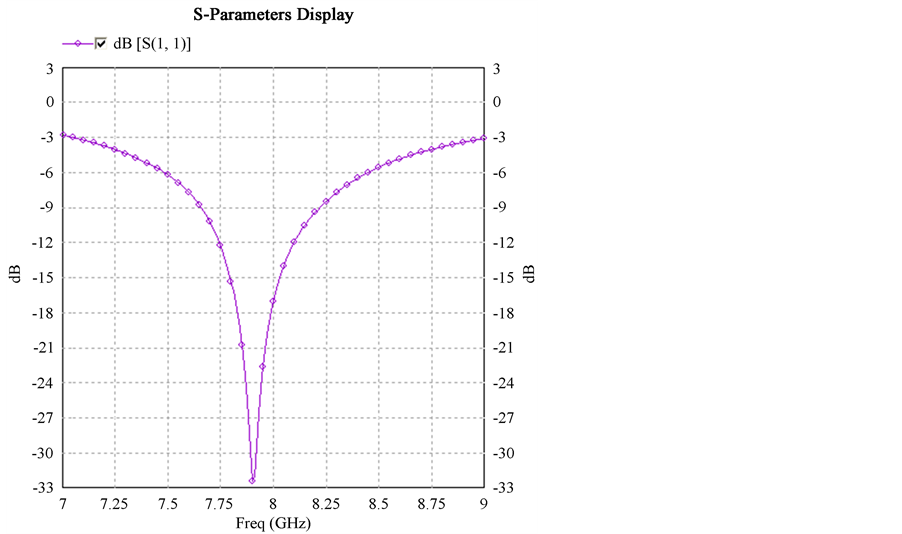
The S-parameters of this design is shown in Figure 9.
The 3-D radiation pattern is sown in Figure 10.
2.5. Antenna with Triple Band-Notch Features
Antenna Description:
To achieve band notch controllability we have taken following steps:
1) Assigning a distinct rejection band for each notching element.
2) Controlling the shape of each element and their optimized positions in order to minimize coupling.
3) Combination of each notch element on the primitive UWB antenna is aimed for providing triple band rejection function at Wi-MAX (3.16 - 3.32 GHz), WLAN 2 (5.3 - 5.72 GHz) and ITU 8 GHz (7.72 - 8.13 GHz).
Figure 5. Geometry of antenna with C-slot to produce band-notch at 5.5 GHz.
Table 3. Measurements of the C-shaped slot (band notch at 5.5 GHz).
Figure 6. Band-notch at 5.5 GHz return loss.
Figure 7. 3D radiation pattern for 5.5 GHz with max gain 2.76 dB.
Design Details:
The measurements of the antenna as well as the measurements of the two C-shaped slots and pair of CSRRs is shown below in Table 5.
The band notch operations are achieved by etching 2 C-shaped slot in the rectangular metal radiating patch and by etching a pair of CSRRs in the ground plane (as shown in the Figure 11). It is found that by adjusting the total length of the C-shaped slot to be approximately half wavelength of the desired notched frequency, a destructive interference can take place, causing the antenna to be non responsive at that particular frequency. It is very easy to tune the notch centre frequency with the change in the total length of the C-shaped slot. More experiments were carried out on the length of the C-shaped slot using the simulation program IE3D.
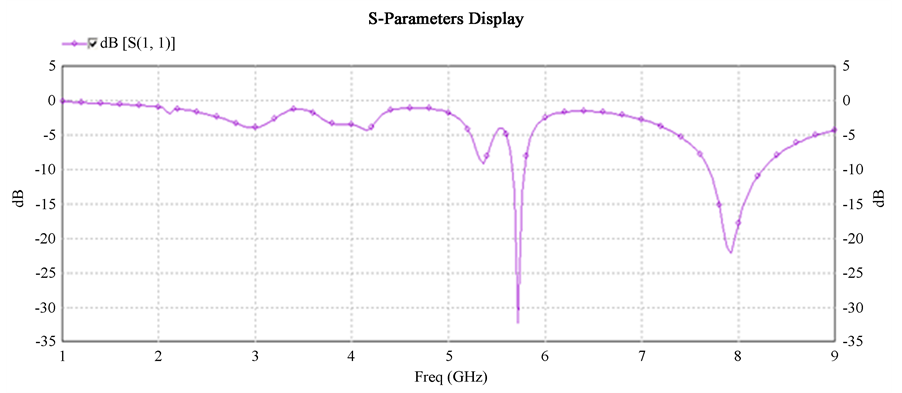
Figure 12 shows the return loss for triple band notched antenna.
Table 4. Measurements of the 2 CSRRs (Complementary Split Ring Resonator) providing us with a band notch at 7.9 GHz.
Figure 8. Geometry of antenna with a pair of CSRRs (notch at 7.9 GHz).
Figure 9. Pair of CSRRs (notch at 7.9 GHz) return loss.
Figure 10. 3D radiation pattern for 7.9 GHz with max gain 4.51 dB.
Figure 11. Geometry of antenna with triple band notch.
This Return Loss graph belongs to the triple band notch antenna, with the band notches at 3.2 GHz, 5.5 GHz and 7.9 GHz. The band notches at the frequency 3.2 GHz and 7.9 GHz is small because of the cross coupling caused due to the integration of all the 3 slots at a time in one antenna.
The 3-D radiation pattern for 3.2GHz is shown in Figure 13.
The 3-D radiation pattern for 5.5 GHz is shown in Figure 14.
The 3-D radiation pattern for 7.9GHz is shown below in Figure 15.
Summary of triple band notched for UWB MSA is shown below in Table 6.
3. Conclusions
This paper proposed design of simple rectangular microstrip antenna for UWB applications. The antenna is capable of achieving multi notched-band. The following points summarized our design:
Table 5. the above table gives us the measurements of the antenna as well as the measurements of the 2 C-shaped slots and a pair of CSRRs.
Figure 12. Return loss for triple band notched antenna.
Table 6. Summary for triple band notched for UWB MSA.
Figure 13. Return loss for triple band notched antenna.
Figure 14. Return loss for triple band notched antenna.
1) To minimize the potential interferences between the UWB system and the narrow band systems, a compact CPW-fed planar UWB antenna with triple band rejection features was designed. First on the basic antenna individual notches are designed and their band-notch properties are studied. Then all the three notches are embedded onto the primitive antenna. While integrating all the notch elements utmost care has been taken to minimize the
Figure 15. 3D radiation pattern for 7.9 GHz with max gain 5.11 dB.
cross-coupling among them; so that their operation doesn’t get hampered by the presence of other notch elements.
2) Antenna operates in the specified 3.1 - 10.6 GHz range and the notches are at 3.2 GHz, 5.5 GHz and 7.9 GHz.
References
- Commission, F.C. (2002) Revision of Part 15 of the Commission’s Rules Regarding Ultra-Wideband Transmission Systems, First Report and Order. ET Docket 98-153, FCC 02-48, 100-118.
- Liang, J., Chiau, C.C., Chen, X. and Parini, C.G. (2004) Printed Circular Disc Monopole Antenna for Ultra-Wideband Applications. Electronics Letters, 40, 1246-1247. http://dx.doi.org/10.1049/el:20045966
- Latré, B., Braem, B., Moerman, I., Blondia, C. and Demeester, P. (2011) A Survey on Wireless Body Area Networks. Wireless Networks, 17, 1-18. http://dx.doi.org/10.1007/s11276-010-0252-4
- Choi, S.H., Park, J.K., Kim, S.K. and Park, J.Y. (2004) A New Ultra-Wideband Antenna for UWB Applications. Microwave and Optical Technology Letters, 40, 399-401. http://dx.doi.org/10.1002/mop.11392
- Mardani, H., Ghobadi, C. and Nourinia, J. (2010) A Simple Compact Monopole Antenna with Variable Single- and Double-Filtering Function for UWB Applications. IEEE Antennas and Wireless Propagation Letters, 9, 1076-1079. http://dx.doi.org/10.1109/LAWP.2010.2091391
- Li, W.-M., Ni, T., Zhang, S.-M., Huang, J. and Jiao, Y.-C. (2011) UWB Printed Slot Antenna with Dual Band-Notched Characteristic. Progress in Electromagnetics Research Letters, 25, 143-151. http://dx.doi.org/10.2528/PIERL11061702
- Dong, Y.D., Hong, W., Kuai, Z.Q. and Chen, J.X. (2009) Analysis of Planar Ultrawideband Antennas with On-Ground Slot Band-Notched Structures. IEEE Transactions on Antennas and Propagation, 57, 1886-1893. http://dx.doi.org/10.1109/TAP.2009.2021910
- Zhang, M., Yin, Y.-Z., Ma, J., Wang, Y., Xiao, W.-C. and Liu, X.-J. (2010) A Racket-Shaped Slot UWB Antennacoupled with Parasitic Strips for Band-Notched Application. Progress In Electromagnetics Research Letters, 16, 35- 44. http://dx.doi.org/10.2528/PIERL10060910
- Chen, W.-S. and Ku, K.-Y. (2008) Band-Rejected Design of the Printed Open Slot Antenna for WLAN/WiMAX Operation. IEEE Transactions on Antennas and Propagation, 56, 1163-1169. http://dx.doi.org/10.1109/TAP.2008.919192
- Gao, G.-P., Mei, Z.-L. and Li, B.-N. (2010) Novel Circular Slot UWB Antenna with Dual Band-Notched Characteristic. Progress in Electromagnetics Research C, 15, 49-63. http://dx.doi.org/10.2528/PIERC10032703
- Lin, Y.-C. and Hung, K.-J. (2006) Compact Ultrawideband Rectangular Aperture Antenna and Band-Notched Designs. IEEE Transactions on Antennas and Propagation, 54, 3075-3081. http://dx.doi.org/10.1109/TAP.2006.883982
- Pandavand, D. and Sethi, S. (2013) Design of Compact Plannar Ultra-Wide Band Antenna with Band-Notched Characteristic. Thesis.


