Journal of Electromagnetic Analysis and Applications
Vol.5 No.4(2013), Article ID:29666,9 pages DOI:10.4236/jemaa.2013.54027
Effective Size Reduction Technique for Microstrip Filters
![]()
1ECE Department, Maharaja Agrasen Instititute of Technology, Delhi, India; 2NIT, Patna, India.
Email: dhirendra_007@rediffmail.com, asok.de@gmail.com
Copyright © 2013 Dhirendra Kumar, Asok De. This is an open access article distributed under the Creative Commons Attribution License, which permits unrestricted use, distribution, and reproduction in any medium, provided the original work is properly cited.
Received January 21st, 2013; revised February 20th, 2013; accepted March 6th, 2013
Keywords: Band Stop Filter; Fractal Structures; Kotch Curve; Low Pass Filters; Open Stub; Step Impedance Network
ABSTRACT
In this paper an effective size reduction technique using fractal structure is suggested. The proposed technique has been applied on a band stop and a low pass filter separately. This technique provides 42% reduction of size for the band stop filter and about 26% for the low pass counterpart. Both the designed structures are fabricated and the measured results are compared with the simulated results. The proposed technique does not require any recalculation or optimization of dimensions of the filter, and is straightforward to implement. The band stop filter is designed for the center frequency of 3 GHz where as the cut-off frequency for low pass filter is 2.5 GHz. A good agreement between the simulated and measured results is observed. A comprehensible explanation of the proposed technique is also provided.
1. Introduction
Filters are a very important component in the microwave and RF communication systems. In the advanced communication systems, a compact filter circuit with better performance is a basic requirement these days. In this paper the band stop and low pass filters are considered to demonstrate the proposed technique. To remove the unwanted frequency bands from the microwave and radio frequency signals a band stop filter (BSF) plays a very important role in wireless communication systems. Thus the BSF have been widely used in several wireless circuits and systems. The low pass filters are the indispensable components in any microwave communication system especially at the receiving end. There are various BSF structures developed using planar substrates to achieve a compact circuit size. A wide band stop filter is proposed by using single quarter wave length resonator with one section of anti-coupled lines with shorted ant other end [1]. Few structures of band stop filter have also been presented using the defective ground with the aim of a compact size of the filter. Defected ground plane with mushroom structures is proposed in [2], where a multilayer structure has been used to achieve a compact structure. Another compact mictrostrip band stop filter based on defective ground structure (DGS) is designed; these DGS units are considered building blocks of the BSF to achieve the band rejection [3]. A small-size Electromagnetic Band Gap (EBG) microstrip structure with triple EBG structures is designed, this EBG structure is based on the main EBG microstrip line with rectangular patches periodically inserted in the line [4]. The spiral resonators also are used to design a band stop filter. This microstrip band stop filter based on spiral resonators can be implemented with small size because of the subwavelength effect of the resonators [5]. In [6], a parallel coupled band stop filter using a double negative coupled transmission line is designed. It requires a shorter coupling to achieve a compact size. A compact band stop filter is also presented using a meander spur line and a pair of capacitive loaded stubs [7].
Using the microstrip line with open end stubs separated with quarter wavelength lines at the center frequency of stop band is one of the most widely used method to design a wide band stop filter [8-10]. This technique is one of the conventional and more widely used methods. These quarter wave length connecting lines are used as unit elements. Since the unit elements of this type of band stop filter are redundant, and their filtering properties are not well utilized, the resultant band stop filter is not an optimum one. For band stop filters the unit elements can be made nearly as effective as the open-circuited stubs. Therefore, by incorporating the unit elements in the design, significantly steeper attenuation characteristics can be obtained for the same number of stubs as is possible for filters designed with redundant unit elements. Also, a specified filter characteristic can be met with a more compact configuration using fewer stubs if the filter is designed by an optimum method [11,12]. This optimum method is used in this paper to design the band stop filter and then the fractal structure [13] is applied on the connecting lines of the open ended stubs.
Similar technique of size reduction is applied on the low pass microstrip filter. The fractal curve has been applied on the high impedance line of the stepped impedance microstrip low pass filter. Using microstrip structure the low pass filter is designed by using either open stub or stepped impedance technique [8,9]. The stepped impedance technique is more common because of its simpler design methodology. The low pass filter design using this technique occupies larger area. To achieve the compact structure several efforts have been made. A compact low pass filter has been designed using slow wave resonators [14], whereas a compact semi lumped low pass filter is proposed in [15]. However the lumped elements raised fabrication difficulties and lumped elements have stray capacitive and inductive effects which affects the desired results. In [16], a low pass filter using a single microstrip stepped impedance hairpin resonator with direct-connected feed lines is proposed, which has the advantage of extending the stop band between the first and second resonant frequency because of the effect of loading capacitance. In [17], a low pass filter using coupled lines is proposed, which has two attenuation poles in the stop band. However, the use of coupled lines reduces the varieties of filter configurations, and then reduces applications of the type of filter. The utilization of microstrip open-loop resonators allows various filter configurations including those of elliptic or quasi-elliptic function response to be realized [18]. In this paper a Chebyshev low pass prototype of order five and pass band ripple is 0.1 dB are considered to design a low pass filter using stepped impedance technique. For the designs, band stop as well as low pass filter, the dielectric constant and height of the substrate considered in this paper is taken as 3.2 and 0.762 mm respectively.
2. Design of Fractal Structure Using Kotch Curve
The basic structure of 1-D, 90˚ angles Kotch curve [13] is taken into consideration for the proposed designs. This fractal curve is shown in Figure 1 up to two iterations. The first iteration is shown in Figure 1(b) and the second iteration is shown in Figure 1(c).
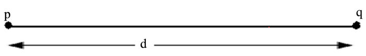
The length of the line that is the distance between the two end points p and q is considered as d which is shown in Figure 1(a). For first iteration the length of the unit section line becomes d/8 which makes the distance between p and q shorter by half that is d/2 in order to make
 (a)
(a)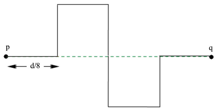 (b)
(b)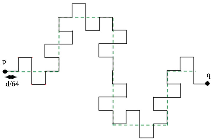 (c)
(c)
Figure 1. Basic structure of the Kotch curve: (a) Zero iteration; (b) First iteration; (c) Second iteration.
the physical length of the line unchanged as shown in Figure 1(b). In similar fashion the distance between p and q becomes d/4 for the second iteration as the length of the unit section line becomes d/64 as shown in Figure 1(c). The structures shown in Figure 1 may be utilized to reduce the lengths of the microstrip filters where long thin microstrip lines are used. It has been applied on two different structures in the presented work where a considerable reduction in lengths has been observed. In both the designs, only first iteration is utilized to avoid the complexity in fabrication.
3. BSF Design Using Fractal Curve
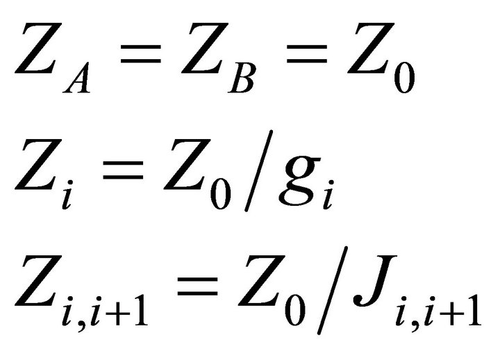
The basic structure of the proposed band stop filter is based on the open circuited transmission line stub network as depicted in Figure 2. Filtering characteristics of this filter entirely depend on the design of characteristic impedances Zi for the open-circuited stubs, and characteristic impedances Zi,i+1 for the unit elements, as well as two terminating impedances ZA and ZB [8,9].
The synthesis of the above shown ladder network
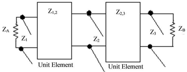
Figure 2. Transmission line network representation of open stub band stop filter.
shown in Figure 2 is based on following transfer function given in Equation (1).
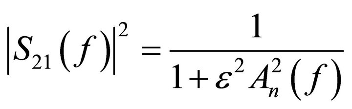 (1)
(1)
where ε is the pass band ripple constant and An is the filtering function represented by the following function
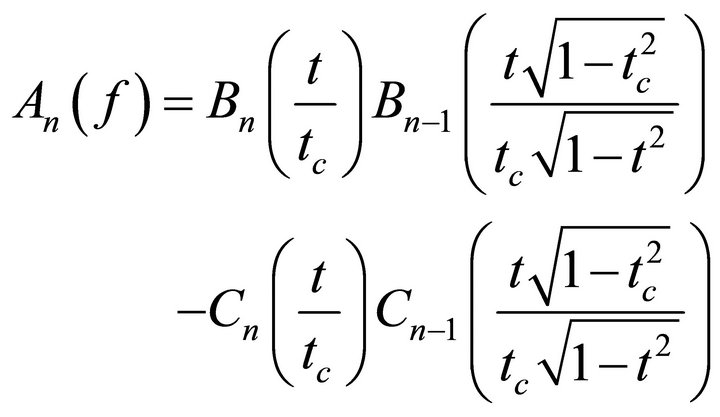 (2)
(2)
where t is the Richards’ transform variable which is given by
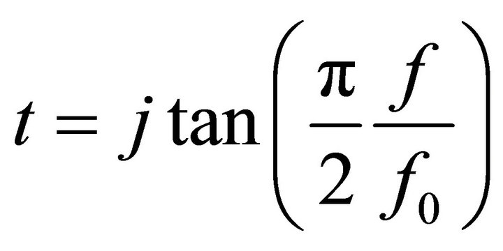 (3)
(3)
 (4)
(4)
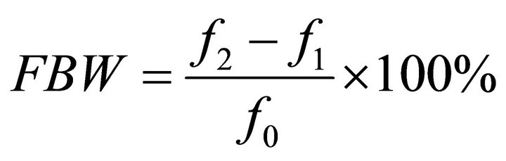 (5)
(5)
where f0 is the mid-band frequency of the band-stop filter and FBW is the fractional bandwidth.  and
and  are the Chebysheve functions of the first and second kinds of order n:
 (6)
(6)
 (7)
(7)
The elemental values are normalized admittances, and for a reference Impedance Z0 = 50 ohm, the impedances are determined by the set of Equation (8).
 (8)
(8)
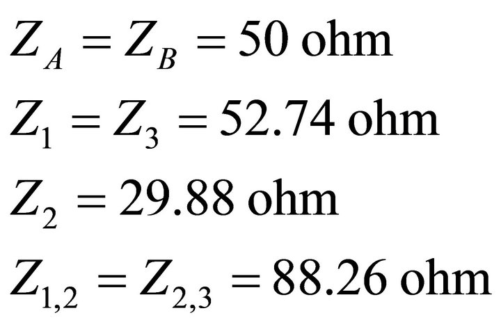
An optimum microstrip band-stop filter with three open-circuited stubs and a fractional bandwidth FBW = 100% at a mid-band frequency  is designed. By considering a pass band return loss of 20 dB, which corresponds to a ripple constant ε = 0.1005. For optimized filter the normalized element values are taken from [9] which are
 , and the impedance inverters as
 . The filter is designed to match 50 ohm terminations. Therefore Z0 = 50 ohm, and from Equation (8) we determine the electrical design parameters for the desired filter network as given below:
The lengths and widths of the corresponding microstrip line open stub filter are determined. The microstrip BSF of such design with their dimensions is shown in Figure 3. The microstrip filter depicted in Figure 3 takes into account the open end and T-junction effects. The width of the microstrip lines connected with two open end stubs are 0.45 mm and width of the 50 ohm microstrip line is 1.82 mm.
The fractal structure shown in Figure 1(b) is now applied in the structure shown in Figure 3. The thin microstrip line is modified using the fractal curve. The proposed filter is depicted in Figure 4. In the modified filter
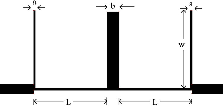
Figure 3. Microstrip BSF with optimum design with a = 0.3 mm, b = 2.3 mm, W = 15.15 mm, L = 15.5 mm.
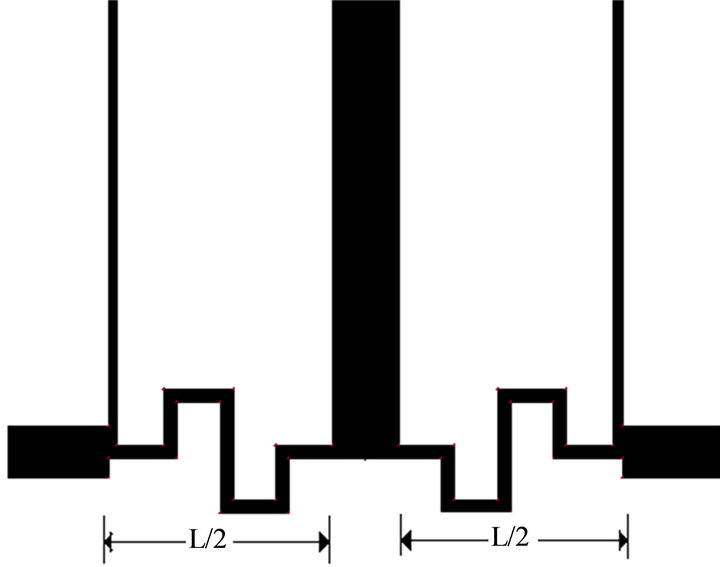
Figure 4. Band stop filter with fractal lines.
there are no change in the dimensions, only the structure of connecting lines are changed. With the application of Kotch fractal the distance between the two open end stubs becomes half. The total length reduction of L = 15.5 mm is achieved.
The simulated results of the modified BSF with fractal structure are compared with the filter without modification. Figure 5 gives the comparison of the S11 parameters of the filter structures shown in Figure 3 and 4. In this result it can be clearly observed that the return loss is very much similar in both the cases. The S21 parameters are also compared for the filters with and without the fractal implementation which is shown in Figure 6. The insertion loss is also similar for both the structures. The proposed design is fabricated using photolithographic technique. The fabricated structure is shown in Figure 7. The S11 and S21 parameters of the fabricated structure are measured using vector network analyzer. Figures 8 and 9 compare the measured values of S11 and S21 respectively of the fabricated structure with the simulated parameters of the structure shown in Figure 4. A very good agreement has been observed between the simulated and tested results as evident from the S-parameters.
Thus the band stop filter using open stubs can be designed in a compact size with no change in the design equations given in [9], only a structural change of fractal curve on the connecting lines are required. From the Figures 5 and 6, it is clear that with a considerable size reduction same response of the band stop filter can be obtained.
4. Low Pass Filter with Fractal Curve
In this section a compact microstrip low pass filter is designed using the fractal structure discussed in Section 2. To design a microstrip low pass filter stepped impedance technique is used in which higher and lower impedances are used to get the effects of inductive and capacitive impedances respectively from the distributive structures. In a microstrip as the impedance of the line increases the width of the line become thinner and vice-versa. So to get the appropriate values of the inductances and capacitances in microstrip
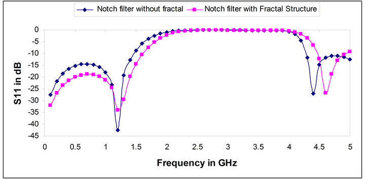
Figure 5. Comparison of S11 parameters of notch filter with and without fractal structure.
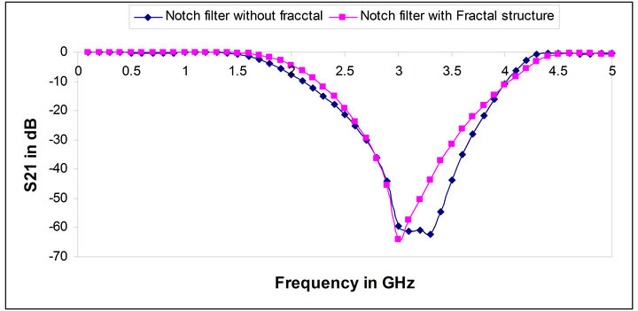
Figure 6. Comparison of S21 parameters of notch filter with and without fractal structure.
the ratio of higher to lower impedance value of lines 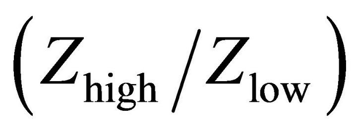 should be as high as possible (where Zhigh and Zlow are the higher and lower impedances of the microstrip lines), but limited by the practical values that can be fabricated on a printed circuit board because very thin line is impractical to fabricate. The typical values are Zhigh = 100 W to 150 W and Zlow = 15 W to 25 W. Since a typical low-pass filter consists of alternating series inductors and shunt capacitors in a ladder configuration, we can implement the filter on a printed circuit board by using alternating high and low characteristic impedance section transmission lines. In this design we have selected Zlow = 24 Ω and Zhigh = 100 Ω. For the filter specification given above following calculations are made. For these low and high impedances the width of the microstrip line is determined as 6.35 mm and 0.48 mm respectively. Also for Z0 = 50 Ω, the width of the transmission line obtained is w = 1.82 mm. The relationship of inductance and capacitance to the transmission line length at the cut-off frequency wc are:

Figure 7. Fabricated structure of proposed band stop filter.

Figure 8. Comparison of measured and simulated values of S11 parameters.
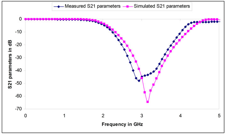
Figure 9. Comparison of measured and simulated values of S21 parameters.
 (9)
(9)
 (10)
(10)
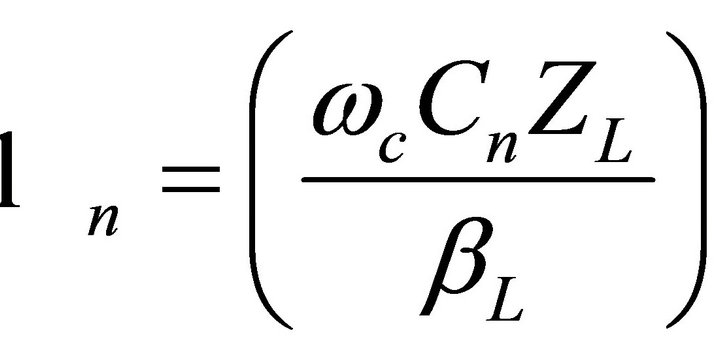
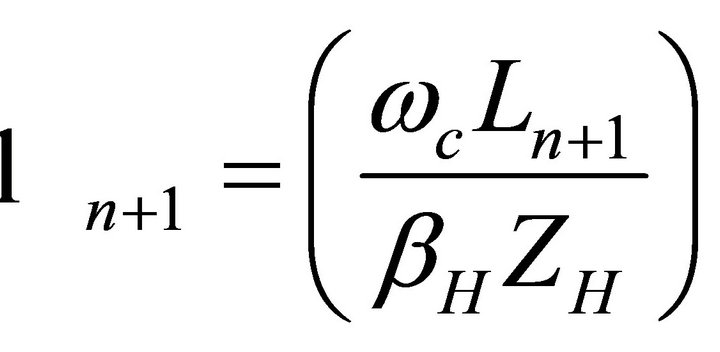
where  and
and  are the physical lengths. Using the design Equations (9) and (10) and the lumped parameter values obtained above, the lengths of the inductive and capacitive lines are determined as below which have been depicted in Figure 10.

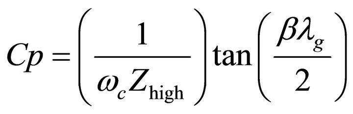
There are stray capacitive and inductive effects produced by high impedance and low impedance lines respectively. By minimizing these effects the circuit size can be made compact [9]. From the Figures 11 and 12 this phenomenon of stray capacitance and inductance can be understand. These effects are minimized by solving the Equations (11) and (12).

Figure 10. Layout of Chebyshev LPF using stepped impedance technique.

Figure 11. Stray capacitance (Cp) in high impedance line.
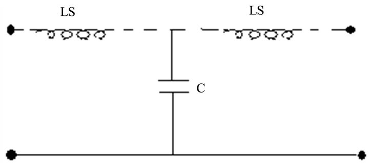
Figure 12. Stray inductance (Ls) in low impedance line.
 (11)
(11)
 (12)
(12)
where Cp and Ls are the stray capacitances and inductances, β is the phase constant, and λg is the wave length of the respective lines. Minimizing the stray capacitance and inductance effects requires a lengthy calculation since it requires number of mathematical iterations and then the lengths of the resonators are needed to be optimized by using the simulation software.
In the proposed method, to reduce the complexity of the design process fractal structure has been applied to the inductive lines of the stepped impedance structure. It has been investigated that by using first iteration and 1/8th order of Kotch curve, the size of filter reduces by more than 26%. By using the fractal shape there is no need to recalculate the dimensions of high and low impedance lines. Using this method there is no need to go for any consideration of end effect or T-junction effects. The designed low pass filter using fractal lines reduces the length of the overall structure by l2 = l4. The proposed structure is shown in Figure 15.
The simulated values of S11 and S21 of the low pass filter with and without fractal structure are shown in Figures 13 and 14. From these S11 and S21 parameters it can be clearly observed that there is no considerable deviation between the values with and without fractal structures. Moreover the pass band characteristics using the fractal structure are slightly improved. The fabricated structure of the proposed design is shown in Figure 16. To provide the close comparison between the tested and simulated results the S11 and S21 parameters are shown in Figures 17 and 18 respectively. From these results it has been observed that there is a good match between simulated and measured values and a slight mismatch is due to the imperfection in fabrication.
5. Conclusion
The proposed method is an effective and efficient size reduction technique with simplicity. This technique of size reduction may be applied on most of the line based microstrip circuits. In the presented work more than 46.5% reduction of the size has been observed without change in the response over the conventional optimized band stop filter. In the case of low pass filter the proposed technique is effective to achieve the compact size with the same response as the conventional low pass filter. The size reduction in the case of low pass filter is more than 26%. This method does not require lengthy calculations or optimization. The proposed technique is
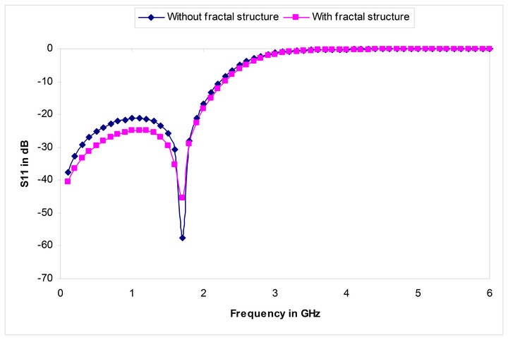
Figure 13. S11 parameters of low pass filter with and without fractal structure.
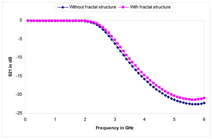
Figure 14. S21 parameters of low pass filter with and without fractal structure.
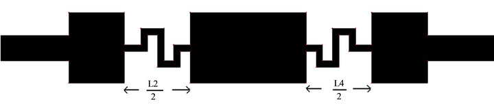
Figure 15. low pass filter with and without fractal structure.

Figure 16. Top view of fabricated structure.
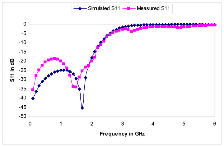
Figure 17. S11 parameters of simulated and measured values of the proposed filter.
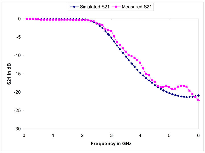
Figure 18. S21 parameters of simulated and measured values of the proposed filter.
verified by comparing the measured results with the simulated results giving good agreement between the two.
REFERENCES
- M.-Y. Hsieh and S.-M. Wang, “Compact and Wideband Microstrip Bandstop Filter,” IEEE Microwave and Wireless Components Letters, Vol. 15, No. 7, 2005.
- Y.-H. Hsu, C.-H. Tsai and T.-L. Wu, “A New Bandstop Filter Using Artificial Defected Ground Structures with Compact Size and Low Radiation” 2010 IEEE 19th Conference on Electrical Performance of Electronic Packaging and Systems (EPEPS), 25-27 October 2010, pp. 89- 92.
- S. U. Rehman, A. F. Sheta and M. Alkanhal, “Compact Bandstop Filter Using Defected Ground Structure (DGS),” 2011 Saudi International Electronics, Communications and Photonics Conference (SIECPC), 24-26 April 2011, pp. 1-4.
- S. Y. Huang and Y. H. Lee, “A Tapered Small-Size EBG Microstrip Bandstop Filter Design with Triple EBG Structures,” Microwave and Optical Technology Letters, Vol. 46, No. 2, 2005, pp. 154-158.
- H. Lim, J.-H. Lee, S.-H. Lim, D.-H. Shin and N.-H. Myung, “A Novel Compact Microstrip Bandstop Filter Based on Spiral Resonators,” Proceedings of Asia-Pacific Microwave Conference 2007, pp. 2221-2224.
- J.-G. Lee and J.-H. Lee, “Parallel Coupled Bandstop Filter Using Double Negative Coupled Transmission Line,” IEEE Microwave and Wireless Components Letters, Vol. 17, No. 4, 2007, pp. 283-285. doi:10.1109/LMWC.2007.892973
- H. W. Liu, R. H. Knoechel and K. F. Schuenemann, “Miniaturized Bandstop Filter Using Meander Spur Line and Capacititively Loaded Stubs,” ETRI Journal, Vol. 29, No. 5, 2007.
- D. M. Pozar, “Microwave Engineering,” 3rd Edition, Wiley, New York.
- J.-S. Hong and M. J. Lancaster, “Microstrip Filters for RF/Microwave Applications,” John Wiley & Sons, Inc, Lancaster RF/Microwave Filter Design, Lancaster, 2001
- B. M. Schiffman and G. L. Matthaei, “Exact Design of Band-Stop Microwave Filters,” IEEE Transactions on MTT-12, 1964, pp. 6-15.
- M. C. Horton and R. J. Menzel, “General Theory and Design of Optimum Quarter Wave TEM Filters,” IEEE Transactions on MTT-13, 1965, pp. 316-327.
- M. C. Horton and R. J. Menzel, “The Effectiveness of Component Elements in Commensurate Line Length Filters,” IEEE Transactions on MTT-16, 1968, pp. 555-557.
- http://en.wikipedia.org/wiki/kotch_snowflake
- C. Jianxin, Y. Mengxia, X. Jun and X. Quan, “Compact Microstrip low pass Filter,” Electronics Letters, Vol. 40, No. 11, 2004, pp. 674-675. doi:10.1049/el:20040481
- J.-W. Sheen, “A Compact Semi-Lumped Low-Pass Filter for Harmonics and Spurious Suppression,” IEEE Microwave and Guided Wave Letter, Vol. 10, No. 3, 2000, pp. 92-93. doi:10.1109/75.845707
- L.-H. Hsieh and K. Chang, “Compact Low Pass Filter Using Stepped Impedance Hairpin Resonator,” Electronics Letters, Vol. 37, No. 14, 2001, pp. 899-900. doi:10.1049/el:20010600
- D. H. Lee, Y. W. Lee, J. S. Park, D. Ahn, H. S. Kim and K. Y. Kang, “A Design of the Novel Coupled Line LowPass Filter with Attenuation Poles,” IEEE MTT-S International Microwave Symposium Digest, Anaheim, 13-19 June 1999, pp. 1127-1130.
- J.-S. Hong and M. J. Lancaster, “Theory and Experiment of Novel Microstrip Slow-Wave Open-Loop Resonator Filters,” IEEE Transactions on Microwave Theory and Techniques, Vol. 45, 1997, pp. 2358-2365.