Engineering
Vol. 4 No. 7 (2012) , Article ID: 20535 , 4 pages DOI:10.4236/eng.2012.47049
Steady State Temperature Study on RF LDMOS with Structure Modification
1National ASIC System Engineering Center, Southeast University, Nanjing, China
2Key Laboratory of Modern Acoustics, Institute of Acoustics, Nanjing University, Nanjing, China
3Department of Electronic System, The Royal Institute of Technology-KTH, Stockholm, Sweden
Email: zixuan19861002@126.com
Received April 19, 2012; revised May 30, 2012; accepted June 7, 2012
Keywords: RF LDMOS; 3D Steady-State Temperature; Die Thickness; Pitch S Length; Finger Width
ABSTRACT
This paper is devoted to temperature analysis on power RF LDMOS with different feature parameters of die thickness, pitch S length and finger width. The significance of these three parameters is determined from temperature comparison obtained by 3D Silvaco-Atlas device simulator. The first three simulations focus on temperature variation with the three factors at different output power density respectively. The results indicate that both the thinner die thickness and the broaden pitch S length have distinct advantages over the shorter finger width. The device, at the same time, exhibits higher temperature at a larger output power density. Simulations are further carried out on structure with combination of different pitch s length and die thickness at a large 1 W/mm output power density and the temperature reduction reaches as high as 55%.
1. Introduction
RF LDMOS has become the most popular RF power technology for base station applications. However, as demand for much higher power level, device temperature increases due to self-heating effects taking place inside the active area. Thus, the electrical characteristics such as reliability and linearity are strongly affected [1,2]. As a result, treatment for thermal effect are mainly from circuit view with compensation network such as adaptive bias [3], predistortion linearizers [4], and multistage RC network [5]. While, in essence, process improvement with structure modification directing to reduce the temperature is a priority to guarantee the performance. A 40 μm ultra-thin RF LDMOS was first reported in [6], which gives a verification of junction temperature reduction. Other structure modification is also tried in today’s device design. The objective of the presented work is a thermal study to compare the significance of changes on die thickness, pitch s length and finger width.
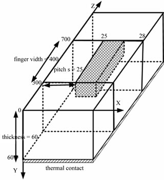
2. Structure Description
A typical structure is illustrated in Figure 1. The active device is located in the middle of z direction from 300 μm to 700 μm. For RF LDMOS, the drift region determines most part of on-resistance and most power consumption generates in this place. Thus, the gridding area in the figure, corresponding to the LDD region, is defined as heat source. The rest area of LDMOS including the p+ sinker, n+ source, gate and drain are all considered as non-heat source area [7].
A half-structure is used to study the temperature distribution for the device symmetry. The feature parameters are as follows: finger width = 400 μm, die thickness = 60 μm, pitch s length = 25 μm and LDD length = 2.5 μm.
Boundary conditions definition is important in thermal simulation [8]. Assume all sides of the structure are insulated except the bottom. This is also reasonable for the middle finger when a multi-finger device under operation is studied. The top surface is adiabatic because the heat dissipation is blocked by the package [9]. The bottom surface, differently, is set to be 300 K corresponding to the heat sinker.
3. Simulation Results
The junction temperature description with electrothermal model is shown as [10]:
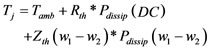 (1)
(1)
The instantaneous dissipated power determines the instantaneous rate of heat that is applied to the transistor. Thermal resistance describes the steady state temperature
 (a)
(a) (b)
(b)
Figure 1. (a) Typical 3D structure used for thermal simulation; (b) Typical cross section of LDMOS used for thermal simulation.
and thermal capacitance expresses the dynamic behavior. The dynamic behavior only needs to be accounted for small tone spacing. The steady character related to the thermal resistance is determined by the device structure.
3D thermal distribution simulation is implemented in Silvaco-Atlas. The steady-state lattice heat diffusion is given as:
 (2)
(2)
where T represents the steady-state temperature, k represents the thermal conductivity and q represents the power generation per unit volume in the heat source.
The thermal conductivity is generally temperature dependent and can be described by:
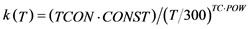 (3)
(3)
TCON.CONST is set to be 1.55 and TC.NPOW is –1.33. Atlas affords an accurate numerical simulation to predict the temperature distribution in a 3D structure. The typical LDMOS has an output power of 0.7 W per mm of gate width. Assume the device efficiency is 60%, the heat source is easily computed to be 0.1867W for the 400 μm finger width device.
Simulation results of the temperature distribution across the top surface are shown in Figure 2(a). From the z direction view, the middle locations have obviously higher temperature over other places. The highest temperature reaches 311 K while it decreases slowly close to 300 K at edges. The highest temperature comes nearly to the drain and it can be clearly observed in Figure 2(b) which gives a temperature distribution of cross section located at z = 500 μm. In this figure, the temperature drops quickly and reaches 300 K at the bottom.
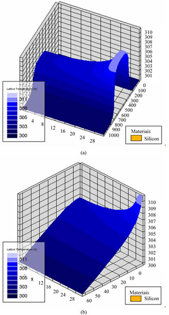
Figure 2. (a) Temperature distribution of top surface; (b) Temperature distribution of cross section.
A 9-finger device model is further simulated for thermal distribution research. Each finger represents the two adjacent LDD regions which mean the thermal source area. The space between each finger is mainly pitch s area.
A bell-like temperature distribution is obviously appeared in the device, show in Figure 3. For the finger in the middle location, a higher temperature can be observed which attribute to the superposition effect in the middle place.
4. Structure Modification and Discussion
To make the temperature rolling down, structure modification can be an option way to improve the device thermal performance. In our research work, the structure is
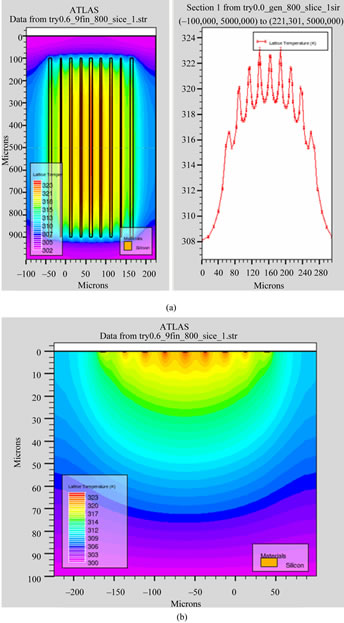
Figure 3. (a) Top surface temperature distribution of a 9- finger device; (b) Cross section temperature distribution of a 9-finger device.
modified with different die thickness, pitch S length and finger width. According to the present process level, output power density is assumed to change from 0.6 W/mm to 1 W/mm, with a step of 0.1 W/mm. We trace the highest temperature changes with all these structure modifications and the results are shown in Figures 4-6.
Figure 3 shows die thickness influence on thermal. Due to the technology at the moment, the thinnest die thickness is confined to 40 μm. The die thickness in this simulation decreased from 100 μm to 40 μm with a step of 20 μm while the finger width and the pitch area are set to be the typical values. Thickness reduction can effectively reduce the temperature especially at high output power density. For the 1 W/mm device, the highest temperature of the 100 μm device is 322.44 K while the 40 μm device is 312.46 K. The reduction is as large as 9.98 K, which reduces 44% heat. Even for the 0.6 W/mm device, the difference is 5.77 K, also reducing the temperature nearly 44%. Making a thinner die is a good way to reduce temperature. Meanwhile, it doesn’t require more surface area. Thus, the whole output power can remain the same.
Figure 5 plots temperature changes with different
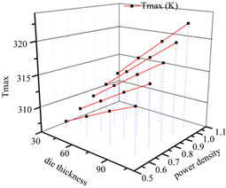
Figure 4. Temperature variation with die thickness and power density.
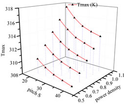
Figure 5. Temperature variation with pitch s length and power density.
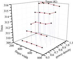
Figure 6. Temperature variation with different finger width and power density.
pitch S length. The trend follows a reasonable way that large S area has a lower temperature. This can be easily understood for the large area of heat dissipation and thermal contact. Increasing the pitch length causes the device occupying a larger area and it’s not benefit for circuit designers. In our study, the longest pitch S is considered to be 40 μm. Variation is changed from 25 μm to 40 μm with a step of 5 μm and the die thickness and finger width remain at the typical value. The highest temperature reaches up to 317.55 K and it can be reduced by 3.88 K with an increase of 15 μm on pitch s length. For the 0.6 W/mm device considered, the highest temperature 310.33 K can also be reduced by 2.33 K, accounting for 22%. This ratio is almost the same as in the 1 W/mm device. Increasing the pitch S area is another optional approach to reduce the temperature. Besides, it’s much easier for technology processing.
Increasing the finger width may introduce more parasitic capacity, but at the same time, it can afford more power output. So, the study of temperature change with different finger width is also important. Figure 6 gives a description of finger width changes from 400 μm to 800 μm with a step of 100 μm. Die thickness and pitch S are fixed to typical dimensions. From the figure, we can hardly find any temperature change with finger width, even for the largest output power of 1 W/mm device. So, finger width adjustment is no useful when temperature is the only factor concerned.
The above three structure study has found the thinner die thickness and larger pitch area have benefit for thermal especially at high output power density. To further figure out these two factors affection, we study the simulation with different combinations. A 1 W/mm device is selected to complete the temperature variation. A more obvious temperature change appears in Figure 7. With a 100 μm die thickness and 20 μm pitch S length, the device temperature grows up to 325.47 K. Combination with 40 μm die and 40 μm pitch S, this temperature drops to 311.45 K, reducing by 55%.
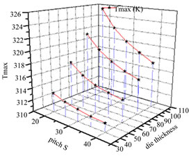
Figure 7. Temperature variation under 1 W/mm output power density.
5. Conclusion
To give instructions for device designer, a temperature study on LDMOS with different die thickness, pitch S length and finger width is presented in this work. Temperature distribution is obtained with the numerical me thod integrated in Silvaco. The simulation results indicate a 44% and 22% temperature reduction with modifycation on die thickness and pitch S length respectively. Increasing the finger width, on contrast, has no advantage for cooling down the temperature. For a device with 1 W/mm output power density, the most effective combination with 40 μm die thickness and 40 μm pitch S length, the highest temperature drops by 55%.
6. Acknowledgements
This work was supported by the IEB ES 64330 for Thermo-Electric Generator, funded by Vinnova FFI program.
REFERENCES
- M. A. Belaid, K. Ketata, K. Mourgues, H. Maamame, M. Masmoudi and J. Marcon, “Comparative Analysis of Accelerated Ageing Effects on Power RF LDMOS Reliability,” Proceedings of the 16th European Symposium on Reliability of Electron Devices, Failure Physics and Analysis, September-November 2005, pp. 1732-1737.
- M. A. Belaid, K. Ketata, K. Mourgues, M. Gares, M Masmoudi and J. Marcon, “Reliability Study of Power RF LDMOS Device under Thermal Stress,” Microelectronics Journal, Vol. 38, No. 2, 2007, pp. 164-170. doi:10.1016/j.mejo.2006.08.004
- S. Y. Chen and J. S. Yuan, “Adaptive Gate Bias for Power Amplifier Temperature Compensation,” IEEE Transactions on Device and Materials Reliability, Vol. 11, No. 3, 2011, pp. 442-448. doi:10.1109/TDMR.2011.2160264
- S. Boumaiza, “Thermal Memory Effects Modeling and Compensation in RF Power Amplifiers and Predistortion Lineaizers,” IEEE Transactions on Microwave Theory and Techniques, Vol. 51, No. 12, 2003, pp. 2427-2433. doi:10.1109/TMTT.2003.820157
- Y. Takahashi, R. Ishikawa and K. Honjo, “Precise Modeling of Thermal Memory Effect for Power Amplifier Using Multi-Stage Thermal RC-Ladder Network,” Asia Pacific Microwave Conference, 12-15 December 2006, pp. 287-290.
- J. A. Herbsommer, H. Safar, W. Brown, P. Gammel, O. Lopez and G. Terefenko, “Improved Electrical and Thermal Performance of Ultra-Thin RF LDMOS Power Transistors,” Microwave Symposium Digest, 2003 IEEE MTT-S International, 8-13 June 2003, pp. 213-216.
- J. Roig, D. Flores, J Urresti, S Hidalgo and J Rebollo, “Modeling of Non-Uniform Heat Generation in LDMOS Transistors,” Solid State Electronics, Vol. 49, No. 1, 2005, pp. 77-85. doi:10.1016/j.sse.2004.06.016
- Y. C. Gerstenmaier, A. Castellzzi and G. K. M. Wachutka, “Electrothermal Simulation of Multichip Modules with Novel Transient Thermal Model and Time-Dependent Boundary Conditions,” IEEE Transactions on Power Electronics, Vol. 21, No. 1, 2006, pp. 45-55. doi:10.1109/TPEL.2005.861116
- A. Ramman, D. G. Waller and T. S. Fisher, “Simulation of Nonequilibrium Thermal Effects in Power LDMOS Transistors,” Solid State Electronics, Vol. 47, No. 8, 2003, pp. 1265-1273. doi:10.1016/S0038-1101(03)00066-2
- J. H. K. Vuolevi, T. Rahkonen and J. P. A. Mannien, “Measurement Technique for Characterizing Memory Effects in RF Power Amplifiers,” IEEE Transactions on Microwave Theory and Techniques, Vol. 49, No. 8, 2001, pp. 1383-1389. doi:10.1109/22.939917