Materials Sciences and Applications
Vol.4 No.12(2013), Article ID:40537,8 pages DOI:10.4236/msa.2013.412101
Conduction Mechanism Analysis of Inversion Current in MOS Tunnel Diodes
![]()
Department of Physics, Yildiz Technical University, Istanbul, Turkey.
Email: *ozdemir@yildiz.edu.tr
Copyright © 2013 Ayşe Evrim Saatci et al. This is an open access article distributed under the Creative Commons Attribution License, which permits unrestricted use, distribution, and reproduction in any medium, provided the original work is properly cited.
Received October 14, 2013; revised November 16, 2013; accepted November 30, 2013
Keywords: Excess Capacitance; MOS; Selfly Inverted Region; Tunneling Based Inversion Currents
ABSTRACT
Self inversion issue and excess capacitance phenomenon were observed for the first time in relatively thick silicon dioxide (SiO2) in the form of MOS (metal(Al)/SiO2/p type crystalline silicon) structure. Both phenomena were based on minority carriers (electrons in this case) and studied through DC current-applied bias voltage (I-V) and AC admittance measurements in dark/light condition as a function of ambient temperature (295 - 380 K). Either of the cases was the departure of traditional MOS analysis, manifesting themselves in the inversion regime of MOS diode. Increase in frequency/temperature/light intensity within dark and light conditions led to weaken the maxima of hump in C-V curves and finally turned into deep depletion mode after exceeding threshold value of frequency/temperature/light intensity. In resumed conditions, supplementary I-V measurements were carried out to describe the generation and conduction mechanism(s) for minority carriers (electrons).
1. Introduction
Electrical properties of Metal-Oxide-Semiconductor (MOS) tunnel diodes, MOSTD, have been attractive due to technological and fundamental physical viewpoints. Though the scaling down of c-MOS integrated circuits leads to significant tunneling current and is a major concern, it also provides an opportunity to study transport phenomena in order to be utilized in light emitting diodes (LED) [1,2] photodetectors [3] and solar cells [4-6].
Inversion region is composed of minority carriers and measured inversion current of MOS diodes could be originated through band to bulk trap and/or band to band tunnelling, and interface state tunnelling [7,8]. Self inversion in MOS structure beyond the gate electrode is a last minority carrier generation model [9-13]. Usually, tunnelling rate and/or generation rate of minority carriers determine the amount of current flowing in MOSTD’s where the semiconductor surface is inverted near zero bias [14,15]. As the applied reverse bias increases, inversion regime becomes strong and hence tunneling current increases abruptly. In the forward direction, the semiconductor goes first from inversion to depletion and then depletion to accumulation regimes as applied bias is scanned from negative to positive bias side. The transition of defined regimes for MOS structure appears as a hump in current-bias voltage (I-V) curves and marks the semiconductor limited to tunnel limited behavior. This kind of hump in I-V curves is also observed in hydrogenated amorphous silicon (a-Si:H)/c-Si [16], micro c-Si/ c-Si [17], and silicon quantum dots embedded in SiO2 insulator film/Si [18,19] structure.
Recently, Lin et al. [20] discussed the generation rate of electron-hole (e-h) pairs in Aluminum(Al)-SiO2- p/p+/p++-c-Si MOSTD’s where p+/p++ represents high doping concentrations of c-Si (above 1018 cm−3). Their observations show that the generation rate of e-h pairs is mainly limited via band to traps tunneling and band to band tunneling rather than conventional Schockley-ReadHall (SRH) statistic model [21,22]. Noteworthy, the transition of band to bulk trap tunneling in depletion layer of c-Si into band to band tunneling through interface traps also exhibits a hump in both computed and experimentally determined I-V curves. Furthermore, band to traps and band to band tunneling models are identified by determining the value of activation energy (EA) as well as their dependences on temperature/light illumination.
Correponding to the hump in I-V curves, theoretical as well as experimental analysis of MOSTD’s indicates similar hump behavior in capacitance-voltage (C-V) curves [7,8,14,15] in minority carrier devices. The onsets and breaking off of hump in capacitance correspond to the transition from semiconductor-limited to tunnel-limited behavior as in I-V curves. Moreover, it is explored that hump has both frequency and work function dependent on chosen metal as electrodes since metals having a low work function like magnesium (Mg) invert the insulator/semiconductor interface at zero bias [7,8,14, 15].
This work discusses the self inversion issue and excess capacitance phenomenon observed for the first time in relatively thick insulator film within MOS structure. In self inversion, minority carriers pile up at SiO2/p-c-Si interface without applying external bias voltage. Those pre-existent electrons could be originated from either ion migration along the surface of insulator during application of prolonged bias voltage or proton diffusion adjacent to insulator/semiconductor interface within a moisture ambient. Due to the electrons, surface bands are bent, creating inversion regime without external bias voltage. Drastic influence takes place especially in this regime of MOS structure such that quasi-static C-V curve is observed for a huge ac modulation frequency (above 100 kHz). This kind of C-V behavior manifests itself as conductivity modulation in I-V measurement and getting such behavior is owing to the injection of minority carrier into the depletion region of junction. Consequently, an extra hole should be supplied to conserve the neutrality conditions, leading to change of the resistivity of diode. Such findings appear as conductivity modulation in I-V measurement and excess capacitance in C-V measurement. Within this context, integrated self inversion issue and excess capacitance phenomenon are considered to interprete anormal C-V feature in inversion regime of MOS structure at hand.
2. Film Fabrication and Experimental Tools
Boron doped and (100) oriented silicon (p-Si) wafer, grown by Czochralski method with 1 - 3 W cm resistivity and 400 µm thicknesses was cleaned chemically via RCA cleaning procedure prior to oxidation. SiO2 insulator film was grown thermally at 1000˚C with dry oxygen (O2) which flew with a constant rate of 600 sccm for 120 min. Backside was coated with Al when the system was pumped down to 10−6 Torr. Then, wafer was annealed to have ohmic contact at 590˚C under N2 ambient for 15 min. Finally, gate (front) electrode of the diodes was formed directly by evaporating Al through copper masks of diameter around 0.1 cm to obtain MOS structure.
For electrical analysis, I-V measurement was performed as a function of temperature in the range between 295 K and 380 K in dark/light condition by Keithley 6517A multimeter. Light illumination was carried out by tungsten lamp. In resumed conditions, capacitance (C) and conductance/frequency (G/ω) as a function of dc gate bias voltage (VG) and its ac voltage modulation frequency (ω) were performed by HP4192A Impedance Analyzer (400 Hz to 1 MHz). Computer controlled LABWIEW program was facilitated to conduct measurements.
3. Results and Discussion
3.1. Dark/Light Current-Voltage Measurement at Room Temperature
Figure 1(a) depicts the I-V variation of Al/SiO2/p-cSi/Ohmic Al MOS tunnel diode in dark and different intensity of light exposure at room temperature. The characteristic with Al as gate electrode demonstrates a consistent minority carrier behavior under small forward and reverse biases [7,8,14,15]. As clear from Figure 1(a), three distinctly different conduction mechanisms are eventual under positively applied gate bias region: under low bias region where V is less than 1 V, sharp increase in current with applied voltage is observed. For the intermediate bias voltage region, 1 < V < 2.5 V, rate in increase reduces and becomes sharp again when V exceeds 3.5 V, exhibiting the onset of last conductive region. These regions illustrate the variation of transport mechanisms in dark I-V curve. Under weak (15 mW/cm2) and strong light illumination (100 mW/cm2), current in negative applied bias shows no drastic change. For the positive side, on the other hand, transition of one to another mechanism becomes smoother and subsequently light insensitive regions comes up around 7.5 V under dark/illuminated condition.In brief, temperature dependent I-V characteristics are required to determine governing generation/conduction mechanisms.
3.2. Temperature Dependent Current-Voltage Measurement
Figure 1(b) shows the small forwad dark I-V-T characteristics within the studied temperature interval of 295 - 385 K. In junction limited case, measured current follows the diode equation:
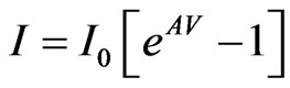 with
with 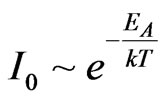 (1)
(1)
where I0 = saturation current, A = temperature (in) dependent factor, k = Boltzman constant. Through fitting of I-V curves, I0 and A are extracted and results are given in Table 1. Insignificant A variations with temperature are obvious. Moreover, Arrhenius plot of I0 versus q/kT
Table 1. Extraction of I0 and A parameters under small forward and reverse bias voltages to deduce the conduction mechanisms and activation energy.
leads EA as 0.63 eV. Furthermore, from the temperature insensitive of A(=q/nkT), ideality factor (n) is determined around 11, designating large amount of interface states in SiO2/p-c-Si structure [23]. Dark IR-VR characteristic with temperature as parameter is given in Figures 1(c) and (d). In there, conductive regions become more clear than in Figure 1(a) where jump in measured current is eventual. For the first and second bias regions, I0 vs q/kT leads EA as 0.68 and 0.25 eV, respectively. For the last region where V > 4V, the relation of I and V is described as
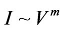 (2)
(2)
where m depends on density of states. Such a characteristic behavior proposes space-charge-limited-current (SCLC) mechanism [24]. Indeed, as given in Figure 1(d), m is extracted from log-log plot of IR-VR characteristic and it alters from 7 to 4 as T changes from 295 to 378 K. Determined EA is also in agreement with that of the published work by Lin et al. for Al-SiO2-p-c-Si MOSTD’s. Retrieved EA by Lin et al. is bias independent in reverse side of dark I-V measurement but it decreases under different illuminations; from nearly half of the c-Si band gap (0.640 eV) to lower values (0.136 eV) [20]. That is the inversion current is comprised of thermal generating current and photo-generated current originated through interface traps and the traps in deep depletion region. Keep in mind that these mechanisms are competing under illumination and temperature dependence becomes insignificant when illumination intensity increases.
Similar observations are made by us on relatively thick SiO2 insulator film where film thickness is determined around 100 nm by high frequency C-V measurement on the Al/SiO2/p-c-Si/Ohmic Al MOS structure. Two competing mechanisms for electron/hole generation processes are observed under low illumination (15 mW/cm2). Moreover, through Arrhenius analysis, EA is obtained around 1 eV from the low bias voltage side under illumination. However, once illumination intensity becomes strong (100 mW/cm2), minority carriers due to light exposure becomes dominant and temperature increase within such condition is surpassed to create e-h pairs. The experimental findings as electron generating mechanisms as well as tunneling process at SiO2/p-c-Si interface are schematically illustrated in Figure 2. In dark, electrons are generated either through a bulk trap within depletion region by process A or over interface traps denoted as process B in Figure 2. Determined EA reveals that minority carrier generation takes place through the process A. In reverse bias, emerged electrons are directed towards SiO2 and then flow by tunneling. In strong inversion, band to band tunneling occurs as proposed by Lin et al. Under light exposure, since EA is found around 1 eV, electrons seem to be excited to the conduction band directly. As inferred from dark/light illuminated I-V-T analysis, current transport mechanisms are unveiled that is nothing but predicted conduction paths in Figure 2. As a consequence of that described conduction paths yield excess capacitance issue in C-V measurement. Therefore, the subsequent section is devoted to debate C-V measurement within resumed condition to complete the analysis.
3.3. Characterization in Dark/Illuminated Condition
Figure 3(a) displays dark capacitance-gate bias (C-VG) variation as a function of modulation frequency (0.7 kHz-1 MHz) of the present diode at room temperature. The insets of Figure 3(a) displays “low” and high frequency C-VG variations. As gate bias is scanned from more negative to more positive side, frequency/bias independent saturated capacitance begins to decrease. Without frequency dependent, saturated capacitance and its reduction in value as gate bias grows towards more positive side is well known: the former corresponds to oxide capacitance, Cox(=eoxA/dox) while decrease in its value is interpreted as the expansion of depletion layer. However, two minimum in inversion capacitance together with hump behavior at high frequency and quasi-static C-V feature as well as excess capacitance at “low” frequency (around 1 kHz) can not be explained as to conventional MOS theory.
 (a)
(a)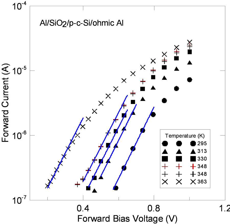 (b)
(b)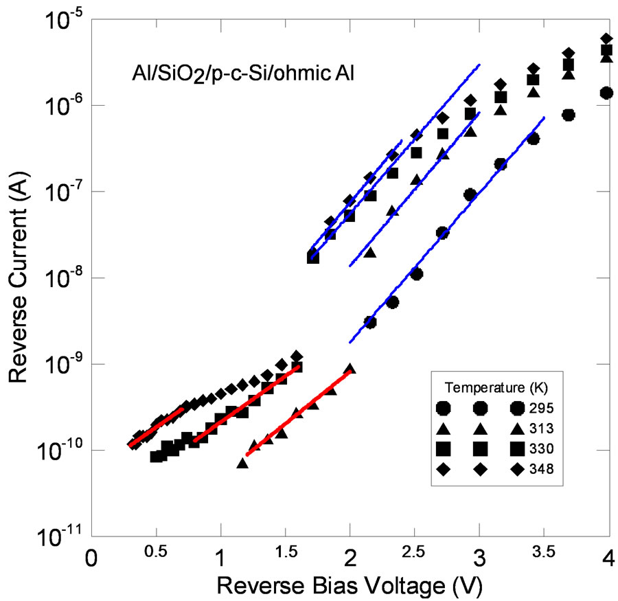 (c)
(c)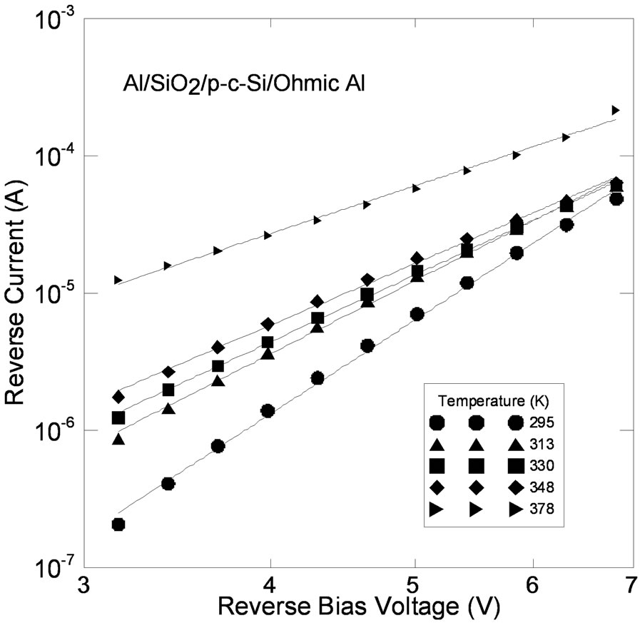 (d)
(d)
Figure 1. (a) Current-applied gate bias variation of Al/SiO2/p-c-Si/Ohmic Al MOS structure in dark and different intensity of light exposure at room temperature. (b) Dark current-bias voltage variation as a function of temperature in between 295 K and 380 K. Solid lines are fitted to experimental data and indicate temperature invariant factor, denoted as A in the body of the work. (c) Dark reverse current-reverse bias characteristic with temperature as parameter. Variation of conduction mechanisms appear as jump in the curves. Also note that fits to experimental data (solid lines) are temperature invariant. (d) Log-log plot of current-bias voltage characteristics within studied temperature interval for VR > 4 V. All fits (solid lines) showed a constant bias power (m) with greater than 2.
Room temperature C-V characteristics under high frequency are consistent with the published work on MOSTD’s. Both hump behavior in C-V and inversion regime under zero bias are expected and experimentally observed on Al/SiO2/p-c-Si MOS minority carrier device. The former demonstrated the transition of semiconductor-limited to tunnel-limited behavior while the latter occurs because of low work function which inverts the interface of SiO2/Si structure. Additionally, frequency dispersion of the hump is also a characterictic feature in MOSTD’s.
Self inversion issue is capable of explaining quasistatic C-V feature under high frequency in present diodes [10,21,22] and MOS diodes featuring silicon nanocrystals in SiO2 matrix [18-19]. In brief, self inversion is a coupling of internal and external inversion layers, respectively: the former is owing to applied inverting gate biases beneath the gate electrode and the latter is formed
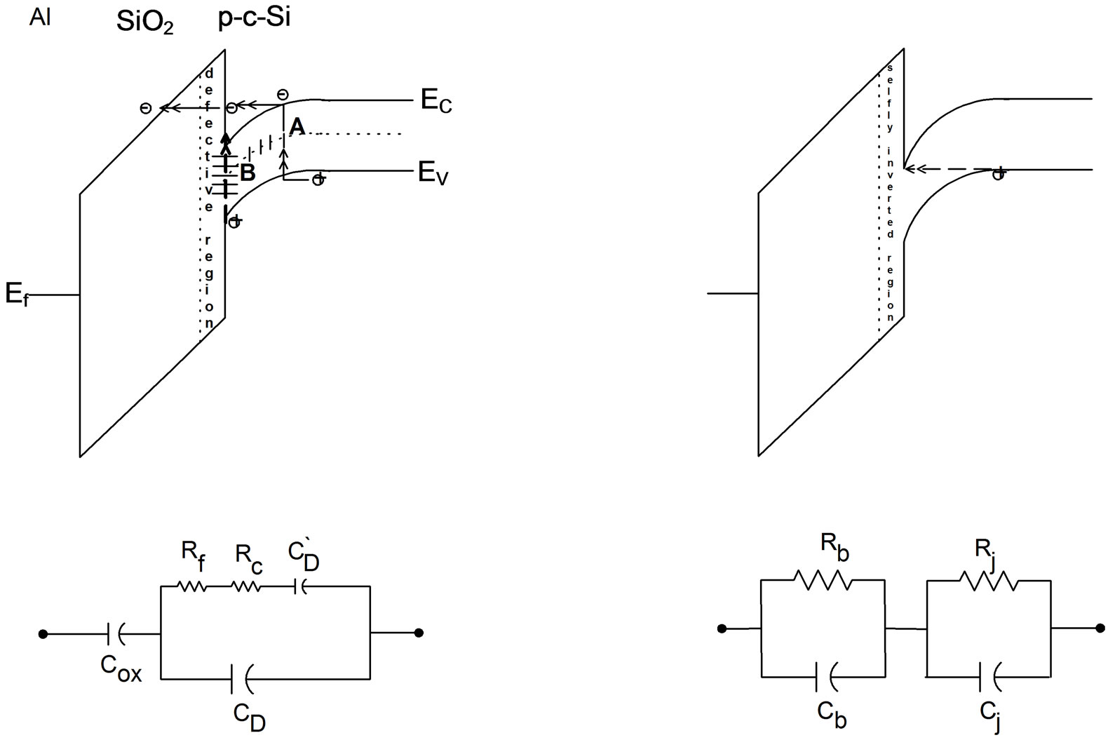
Figure 2. Schematic illustration of minority carrier conduction path, denoted as A through bulk trap in depletion region and B via interface traps. Equivalent circuits display self inversion in MOSTD’s and excess capacitance for n-p junction. Note also that Rc and Rf represent internal/external inversion layers.
beyond the gate electrode and it is originated due to ion migration along the surface of insulator during application of prolonged bias voltage [10,21,22] and/or proton diffusion adjacent to insulator/semiconductor interface [25] within a moisture ambient. Consequently, gate electrode area fictitously is enhanced enormously, enlarging the capacity beyond the gate electrode, CD’. Since measured capacitance is in series combination of Cox and CD + CD’ [9-13], Cox is determined in C-V measurements. On the other side, this channel formation enhances the response time of minority carriers and hence the cutoff frequency of the channel becomes considerably higher than that for minority carriers under equilibrium. In other words, since the relaxation time (τ) of minority carriers would be the product of equivalent resistance and capacitance (τ = RC), minority carriers are in this case able to follow high frequency excitation (more than 50 Hz). As clear from Figure 3(a), this issue resolve only the first frequency dependent portion of the C-V curves in which capacitance rises at most Cox. Nevertheless, the capacitance exceeding Cox is abnormal in terms of MOS analysis and reported only by us as far as we know on MOSTD’s. This kind of C-V behavior is reported in metal/semiconductor Schottky and p-n junctions in which semiconductor could be either crystalline or amorphous [26] phases.
Provided that selfly inverted layer, MOS structure at hand can be considered as n/n+-p junction in which n/n+ layer represent conducting channel at the vicinity of SiO2/Si interface connected in series to a bulk SiO2 insulator film with an huge resistor. Within this frame, the picture matches with the case of intrinsic (i) a-Si:H/p-cSi junction where (i) a-Si:H is slightly n-type doped with 109 Ω cm resistivity. [26]. As bias changes from reverse to forward direction, diffusion capacitance makes a significant contribution over the depletion capacitance of the junction. In other words, diffusion capacitance is in parallel connection with depletion capacitance of the junction. Consequently, measured capacitance begins to increase in value due to the diffusion. As the applied bias increases towards a specific value so does the corresponding capacitance. At the proximity of the specific bias, the measured capacitance is in maxima; for further bias voltage, the capacitance starts to decline. Fall in capacitance from maxima marks the resistive part of a film where SCLC current mechanism is the governing conduction mechanism. Equivalent capacitance and conductance in junction limited case are described as
 (3)
(3)
 (4)
(4)
where Rj(Rb) is junction (bulk) resistance and Cj(Cb) is junction (bulk) capacitance, respectively. In bulk limited case where SCLC current mechanism dominate the carrier conduction, decay in capacitance from maximum can be represented with the relation below:
 (5)
(5)
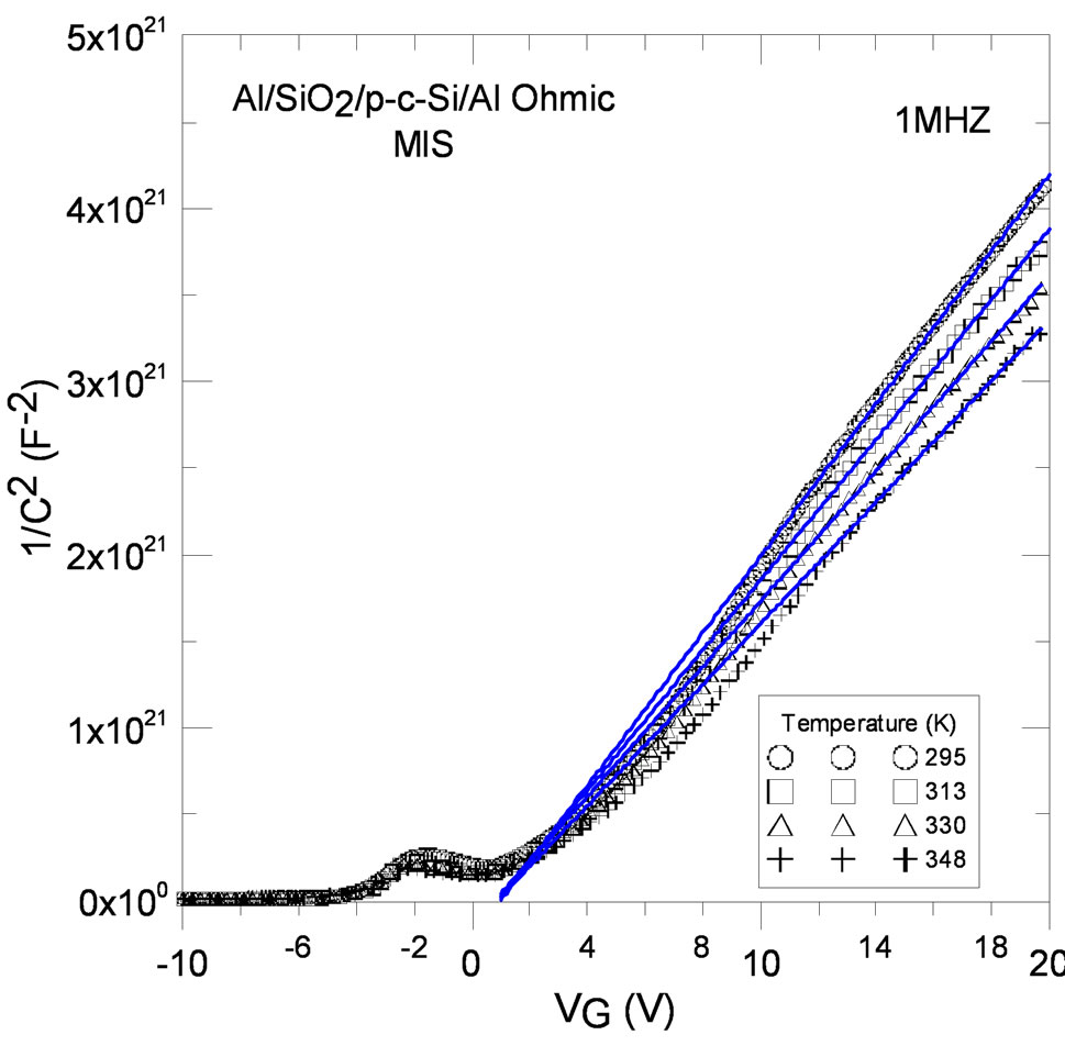
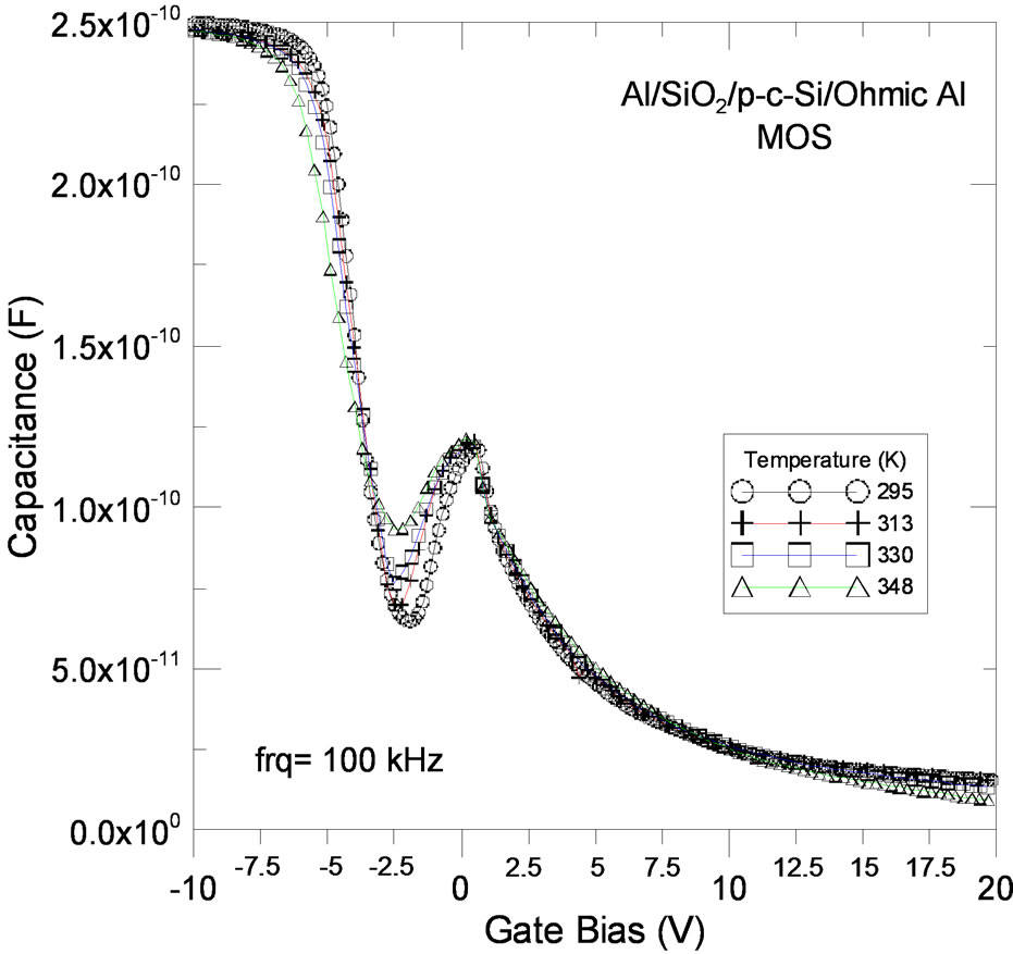
In other words, since depletion width becomes insignificant compared to film thickness in which bulk capacitance is ignored and bulk region is considered purely resistive. In turn, junction limited behavior switches into bulk limited one. The maxima of the hump around 0.9 V might represents either the barrier height of back Al metal electrode for electrons or band bending of SiO2/ c-Si interface. 1/C2-VG curves (given in Figure 3(b)) point both depleting type C-V character and temperature independent built in voltage. Hence, surface band bending should be in maxima. Furthermore, decay in capacitance from maxima corresponds to a well defined bias region (VG > 4 V) where SCLC mechanism is eventual (see Figure 3(b)). As clearly seen in Figure 4, the hump has also temperature/light intensity dependent as in modulation frequency. As ambient temperature/illumination intensity increases, the maxima occurs in lower capacitance valueswhile deep depletion regime in C-VG curves are formed. Within this context, excess capacitance issue, appears as hump in C-V curves under high frequency, is clearly related with current conduction mechanisms or electron generating mechanisms. Electrons due to illumination becomes pile up at the interface and forced to inject into SiO2 film and reach to front electrode through SCLC mechanism. Furthermore, electrons are generated through band to band transition under illumination that is further verified by detemining EA (1.1 eV) through I-V-T measuments in light illuminations (see Figure 2). In admittance counterpart, since the trap loose its charge due to illumination, the electric field is terminated by the charges at the edge of depletion layer and hence deep depletion occurs solely in strong illumination. In dark condition, on the other hand, since the interface is inverted in both beneath and beyond of the gate electrode, the increase in gate bias in positive side do not change the amount of electron concentration but it would be counterbalanced by ionized dopant charges within the depletion layer and hence depletion region becomes widened. As it is widened, depletion capacitance decreases as does measured capacitance.
4. Conclusion
Anamolous C-V behavior at the inverting bias voltage on Al/SiO2/p-c-Si/Ohmic Al MOS tunnel diode was discussed in terms of self-inversion and excess capacitance issues for the first time. These phenomena were capable of exploring unusual C-V features at inverting bias region in which inversion tunneling current in dark ambient was dominated by the thermal generation rate of
 (a)
(a)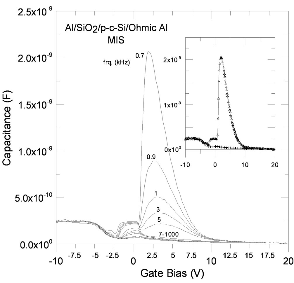 (b)
(b)
Figure 3. (a) Dark C-V characteristic as a function of modulation frequency. The inset of figure display “low” and high frequency C-V characteristics. Note that main frequency dependent regions correspond to self inversion issue and excess capacitance phenomenon, respectively. Except this departures, present diode indicates a traditional MOS regimes; accumulation, depletion, inversion and deep depletion. (b) Dark C−2 versus V variation as a function of ambient temperature at 1 MHz.
 (a)
(a)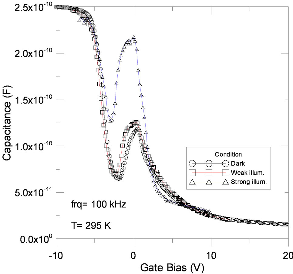 (b)
(b)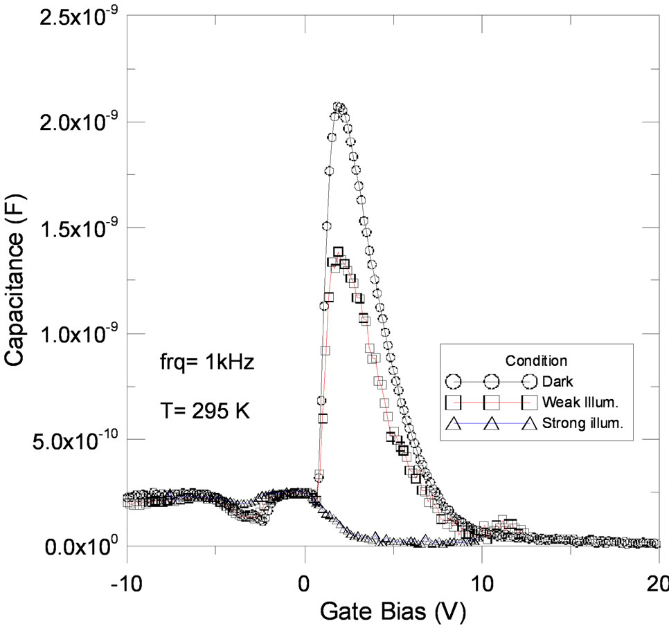 (c)
(c)
Figure 4. C-V variation as a function of temperature in dark (a) and (b) various light intensities under constant frequency (100 kHz). In (c), “low” C-V variation as in (b).
electron-hole couple through interface traps and bulk traps, lying in the depletion region of p type crystalline silicon.
5. Acknowledgements
This work is financially supported by Yildiz Technical University projects under a contract of 2012-01-01- DOP04 and 2011-01-01-KAP03.
REFERENCES
- C.W. Liu, M. H. Lee, M.-J. Chen, I. C. Lin and C.-F. Lin, “Room Temperature Electroluminescence from ElecronHole Plasmas in the Metal Oxide Silicon Tunneling Diodes,” Applied Physics Letters, Vol. 76, No. 12, 2000, pp. 1516-1518. http://dx.doi.org/10.1063/1.126081
- C. W. Liu, M. H. Lee, M.-J. Chen, C.-F. Lin and M. Y. Chern, “Roughness-Enhanced Electroluminescence from Metal Oxide Silicon Tunneling Diodes,” IEEE Electron Device Letters, Vol. 21, No. 12, 2000, pp. 601-603. http://dx.doi.org/10.1109/55.887479
- C. W. Liu, W. T. Liu, M. H. Lee, W. S. Kuo and B. C. Hsu, “A Novel Photodetector Using MOS Tunneling Structures,” IEEE Electron Device Letters, Vol. 21, No. 6, 2000, pp. 307-309. http://dx.doi.org/10.1109/55.843159
- B. Kuhlmann, A. G. Aberle, R. Hezel and G. Heiser, “Simulation and Optimization of Metal-Insulator-Semiconductor Inversion-LayerSilicon Solar Cells,” IEEE Transactions on Electron Devices, Vol. 47, No. 11, 2000, pp. 2167-2178. http://dx.doi.org/10.1109/16.877180
- O. M. Nielsen, “Current Mechanism of Tunnel m.i.s, Solar Cells,” IEEPROC, Vol. 127, No. 6, 1980, Part I.
- O. M. Nielsen, “Current Mechanism of Tunnel MIS Solar Cell,” PROC, Vol. 129, Pt. I, No. 4, A UGUST1982.
- M. A. Green, F. D. King and J. Shewchun, “Minority Carrier MIS Tunnel Diodes and Their Application to Electronand Photo-Voltaic Energy Conversion-I. Theory,” Solid-State Electronics, Vol. 17, No. 6, 1974, pp. 551-561. http://dx.doi.org/10.1016/0038-1101(74)90172-5
- J. Shewchun, M. A. Green and F. D. King, “Minority Carrier MIS Tunnel Diodes and Their Application to Electronand Photo-Voltaic Energy Conversion-II. Experiment,” Solid-State Electronics, Vol. 17, No. 6, 1974, pp. 563-572. http://dx.doi.org/10.1016/0038-1101(74)90173-7
- S. R. Hofstein, K. H. Zaininger and G. Warfield, “Frequency Response of the Surface Inversion Layer in Silicon,” Proceedings of IEEE, Vol. 52, 1964, pp. 971- 972.
- E. H. Nicollian and A. Goetzberger, “Lateral AC Current Flow Model for Metal-Insulator-Semiconductor Capacitors,” IEEE Transactions on Electron Devices, Vol. 12, No. 3, 1965, p. 108. http://dx.doi.org/10.1109/T-ED.1965.15465
- O. Özdemir, I. Atilgan and B. katircioğlu, “Abnormal Frequency Dispersion of the Admittance Associated with a Chromiumplasma Deposited a-SiNx:Hp-Si Structure,” Journal of Non-Crystalline Solids, Vol. 353, 2007, pp. 2751-2757.
- O. Özdemir, I. Atılgan, B. Akaoğlu, K. Sel and B. Katircioğlu, “Frequency Dependence of Conductivity in Intrinsic Amorphous Silicon Carbide Film, Assessed through Admittance Measurement of Metal İnsulator Semiconductor Structure,” Thin Solid Films, Vol. 497, 2006, pp. 149-156. http://dx.doi.org/10.1016/j.tsf.2005.10.065
- O. Özdemir, M. Anutgan, T. Aliyeva-Anutgan, I. Atılgan and B. Katırcioğlu, “Electrical Transport Mechanism in Boron Nitride Thin Film,” Journal of Non-Crystalline Solids, Vol. 355, 2009, pp. 851-859. http://dx.doi.org/10.1016/j.jnoncrysol.2009.04.034
- J. Shewchun and M. A. Green, “Temperature Dependence of Current Flows in Nondegenarate MIS Tunnel Diodes,” Journal of Applied Physics, Vol. 46, No. 12, 1975, pp. 5179-5184. http://dx.doi.org/10.1063/1.322195
- M. A. Green and J. Shewchun, “Capacitance Properties of MIS Tunnel Diodes,” Journal of Applied Physics, Vol. 46, No. 12, 1975, pp. 5185-5190. http://dx.doi.org/10.1063/1.321583
- H. Matsuura, T. Okuno, H. Okushi and K. Tanaka, “Electrical Properties of n-Amorphous/p-Crystalline Silicon Heterojunctions,” Journal of Applied Physics, Vol. 55, No. 4, 1984, pp. 1012-1019. http://dx.doi.org/10.1063/1.333193
- Y. J. Song, M. R. Park, E. Guliants and W. A. Anderson, “Influence of Defects and Band Offsets on Carrier Transport Mechanisms in Amorphous Silicon/Crystalline Heterojunction Solar Cells,” Solar Energy Materials & Solar Cells, Vol. 64, 2000, pp. 225-240. http://dx.doi.org/10.1016/S0927-0248(00)00222-1
- S. Park, E. Cho, D.n Song, G. Conibeer and M. A. Green, “n-Type Silicon Quantum Dots and p-Type Crystalline Silicon Heteroface Solar Cells,” Solar Energy Materials & Solar Cells, Vol. 93, No. 6-7, 2009, pp. 684-690. http://dx.doi.org/10.1016/j.solmat.2008.09.032
- C. Flyn, D. König, I. Perez-Wurfl, G. Conibeer and M. A. Green, “Capacitance and Conductance Characteristics of Silicon Nanocrystal Metal-Insulator-Semiconductor Devices,” Solid-State Electronics, Vol. 53, 2009, pp. 530- 539. http://dx.doi.org/10.1016/j.sse.2009.03.001
- C.-H. Lin, B.-C. Hsu, M. H. Lee and C. W. Liu, “A Comprehensive Study of İnversion Current in MOS Tunneling Diodes,” IEEE Transactions on Electron Devices, Vol. 48, No. 9, 2001, pp. 2125-2130. http://dx.doi.org/10.1109/16.944205
- S. M. Sze, “Physics of Semiconductor Devices”, WileyInterscience, John Wiley & Sons, 1969.
- E. H. Nicollian and J. R. Brews, “MOS (Metal Oxide Semiconductor) Physics and Technology,” John Wiley & Sons, New York, 1982.
- A. E. Saatci and O. Özdemir, “Comparison of Sequentıal and Simultaneous High-Low Frequency Capacitance Voltage Method on MOS Structure,” Balkan Physics Letter, Vol. 18, 2010, pp. 360-367.
- M. A. Lambert, “ Current Injection in Solids,” Academic Press, New York, 1970.
- A. E. Saatci and O. Özdemir, “The Cause of Frequency Response at 100 kHz for the Inversion Regime of MOS Structure,” Proceeding ICCE 2010.
- K. Jerzy “Amorphous and Microcrystalline Semiconductor Devices II Materials and Device Physics,” Artech House, Boston, 1992.
NOTES
*Corresponding author.