Circuits and Systems
Vol.4 No.4(2013), Article ID:35769,17 pages DOI:10.4236/cs.2013.44050
Auto-Scale Factor Circuit Realisation for MIMO Hardware Simulator
Institute of Electronics and Telecommunications of Rennes (IETR), Rennes, France
Email: bachir.habib@insa-rennes.fr
Copyright © 2013 Bachir Habib et al. This is an open access article distributed under the Creative Commons Attribution License, which permits unrestricted use, distribution, and reproduction in any medium, provided the original work is properly cited.
Received April 23, 2013; revised May 23, 2013; accepted June 1, 2013
Keywords: Hardware Simulator; FPGA; MIMO Radio Channel; 802.11ac; LTE
ABSTRACT
A hardware simulator reproduces the behavior of the radio propagation channel, thus making it possible to test “on table” the mobile radio equipments. The simulator can be used for LTE and WLAN 802.11ac applications, in indoor and outdoor environments. In this paper, the input signals parameters and the relative power of the impulse responses are related to the relative error and SNR of the output signals. After analyzing the influence of these parameters on the output error and SNR, an algorithm based on an Auto-Scale Factor (ASF) is analyzed in details to improve the precision of the output signals of the hardware simulator digital block architecture. Moreover, the circuit needed for the validation of this algorithm has been introduced, verified and realized. It is shown that this solution increases the output SNR if the relative powers of the impulse responses are attenuated. The new architecture of the digital block is presented and implemented on a Xilinx Virtex-IV FPGA. The occupation on the FPGA and the accuracy of the architecture are analyzed.
1. Introduction
Tests of a radio communication system, conducted under actual conditions are difficult, because tests taking place on outdoor, for instance, are affected by random movements or even by the weather. Thus, to evaluate the performance of the recent communication systems, a channel hardware simulator is considered. With hardware simulators, it is possible to very freely simulate desired types of radio channels. Moreover, it provides the necessary processing speed and real time performance, as well as the possibility to repeat the tests for any Multiple-Input Multiple-Output (MIMO) system.
Over the past few decades, efforts have resulted in several designs and implementation of real time simulators. Early efforts were based on analog components [1-4]. The development of real time simulator starts in 1973 when in [1] they developed the first Rayleigh based channel simulator. The simulator used Zener diode to generate Gaussian random variable.
However, with the advent of digital computers, fast Analog-Digital Convertors (ADC) and Digital-Analog Convertors (DAC), the analog components were replaced by digital thereby increasing the reliability and flexibility of simulators. In [5], they first used discrete digital logic in its simulator. With the development of Digital Signal Processing (DSP), the DSP based simulators were developed. In [6], they used 16 bit fixed point DSP for implementation and simulated the Gaussian quadrature components along with the log-normally distributed Line-Of-Sight (LOS) component. In [7], they used DSP chips for the development of a narrow-band simulator. In [8], they reported a frequency selective simulator using DSP and integrated circuits. It had a baseband bandwidth of 10 MHz and maximum Doppler frequency of 100 Hz. In [9], they developed 6 taps wide-band channel simulator having maximum signal bandwidth of 20 MHz. It used two 32 bit DSP floating point processors. In [10], they used a hybrid DSP FPGA architecture to build a wide-band channel simulator. It was capable of simulating 12 delay taps and had a baseband bandwidth of 5 MHz. Satellite channel simulator has been developed in [11] using DSP platform. In [12], they developed a narrow-band fast and accurate simulator. In [13], they developed a 5 MHz 12 taps wide-band simulator using 12 DSPs (1 for each tap) for the generation of complex coefficients. A narrow-band DSP based channel simulator has also been developed in [14].
Over the last decade, the use of Field Programmable Gate Arrays (FPGA) in DSP applications has become quite common. With continuing increase of the FPGA capacity, entire baseband systems can be mapped onto faster FPGAs for more efficient prototyping, testing and verification. Larger and faster FPGAs permit the integration of a channel simulator along with the receiver noise simulator and the signal processing blocks for rapid and cost-effective prototyping and design verification. As shown in [15], the FPGAs provide the greatest design flexibility and the visibility of resource utilization. Thus, the FPGA based simulators have also been developed and their implementations have been described [16-23].
Some hardware simulators are proposed by industrial companies like Spirent (VR5) [24] and Elektrobit (Propsim F8) [25]. The commercially available channel simulators may not offer the user enough flexibility when configuring the wireless channel parameters to test the system under different environmental conditions. Moreover, those simulators are often too expensive and therefore prohibitive for communications laboratory. A low cost channel simulator is therefore required that present different environments and provide the user flexibility to measure the performance of the wireless system under real environmental conditions.
MIMO technology has attracted attention in wireless communications, because it offers significant increases in data throughput and link range without additional bandwidth or increased transmit power. It achieves this goal by spreading the same total transmitter power over the antennas to achieve an array gain that improves the spectral efficiency (more bits per second per hertz of bandwidth) and/or to achieve a diversity gain that improves the link reliability (reduced fading). Because of these properties, MIMO is an important part of modern wireless communication standards such as Wireless Local Area Network (WLAN) 802.11ac and Long Term Evolution (LTE). Thus, a 2 × 2 MIMO channel is considered in this paper.
The objective of our work concerns the channel models and the digital block of the simulator. The design of the RF blocks was completed in a previous project [17,26].
The channel models can be obtained from standard channel models, as the TGn IEEE 802.11n [27] and the 3GPP-LTE models [28], or from real measurements conducted with the MIMO channel sounder designed and realized at IETR [29]. In the MIMO context, little experimental results have been obtained regarding timevariations, partly due to limitations in channel sounding equipment [30]. However, theoretical models of impulse responses of time-varying channels can be obtained using Rayleigh fading [31,32].
The MIMO hardware simulator realized at IETR is reconfigurable with sample frequencies not exceeding 200 MHz, which is the maximum value for FPGA Virtex-IV. The 802.11ac signal provides a sample frequency of 200 MHz. Thus, it is compatible with the FPGA Virtex-IV. However, in order to exceed 200 MHz for the sample frequency, more performing FPGA as Virtex-VII can be used [33]. At IETR, several architectures of the digital block of a hardware simulator have been studied, in both time and frequency domains [34,35]. Typically, wireless channels are commonly simulated using finite impulse response (FIR) filters, as in [21,36,37]. The FIR filter output signal is a convolution between a channel impulse response and a fed signal in such a manner that the signal delayed by different delays is weighted by the channel coefficients, i.e. tap coefficients, and the weighted signal components are summed up. The channel coefficients are periodically modified to reflect the behavior of an actual channel. Nowadays, different approaches have been widely used in filtering, such as distributed arithmetic (DA) and canonical signed digits (CSDs) [20].
Using FIR filter in a channel simulator has however a limitation. With a FPGA Virtex-IV, it is impossible to implement a FIR filter with more than 192 multipliers (impulse response with more than 192 taps). To simulate an impulse response with more than 192 taps, the Fast Fourier Transform (FFT) module can be used. With a FPGA Vitrex-IV, the size NF of the FFT module can reach 65536 samples. Thus, several frequency architectures have been considered and tested [20]. However, their disadvantages are high latency and high occupation on FPGA. Moreover, the considered frequency architectures operate correctly for signals not exceeding the FFT size. Thus, new frequency architecture avoiding this limitation has been presented and tested in [38]. In this paper, the number of taps is limited to 18 for each SISO channel, thus, to 18 × 4 taps for the 2 × 2 MIMO channel. Therefore, the time domain architecture is considered because the total number of taps does not exceed 192.
In this paper, the input signals parameters and the relative power of the impulse responses has been related to the relative error and SNR of the output signals. After analyzing the influence of these parameters on the output error and SNR, an improvement algorithm based on an Auto-Scale Factor (ASF) has been proposed and analyzed in details. In fact, to decrease the error at the simulator output signals, it is better to consider a large number of bits in the architecture for the input signal and for the impulse responses. In the context of mobile radio, the input signal and the impulse responses cannot be predicted and they can undergo fading and be strongly attenuated. If they are low, they will not be quantified on a sufficient number of bits. Thus, the error of the output signals of the channel simulator will increase widely. The proposed solution consists on multiplying the input signal and the impulse responses by an ASF that increases the output signals and makes it possible to quantify them on a higher number of bits in order to decrease the error at the output. Moreover, the received signal is divided by the correct ASF to obtain the correct output. Thus, a circuit is introduced which control the input and output signals powers for each sample. The circuit are presented, designed and tested.
Tests are made with input signal that respects the bandwidth chosen between [Ä, B + Ä] and by considering 2 × 2 MIMO architecture. In fact, the channel impulse responses can be presented in baseband with its complex values, or as real signals with limited bandwidth B between fc − B/2 and fc + B/2, where fc is the carrier frequency. In this paper, to eliminate the complex multiplication and the fc, the hardware simulation operates between Ä and B + Ä, where Ä depends on the band-pass filters (RF and IF). The value Ä is introduced to prevent spectrum aliasing. In addition, the use of a real impulse response allows the reduction by 50% of the size of the FIR filters and by 4 the number of multipliers. Thus, within the same FPGA, larger MIMO channels can be simulated.
The rest of this paper is organized as follows. Section 2 presents the channel models used for the test. Section 3 describes the simple and the ASF-based time domain architecture of the simulator digital block. In Section 4, the accuracy of the output signals of the architecture are analyzed in term of occupation on the FPGA and precision of the output signals. Lastly, Section 5 gives concluding remarks and prospects.
2. Channel Description
A MIMO propagation channel is composed of several time variant correlated SISO channels. For MIMO 2 × 2 channel, the received signals yj(t,τ) can be calculated using a convolution :
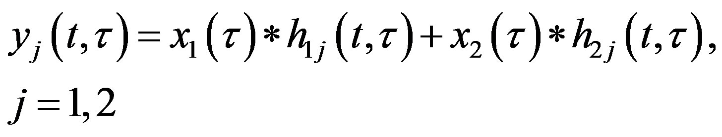 (1)
(1)
The associated spectrum is calculated by the Fourier transform (using FFT modules):
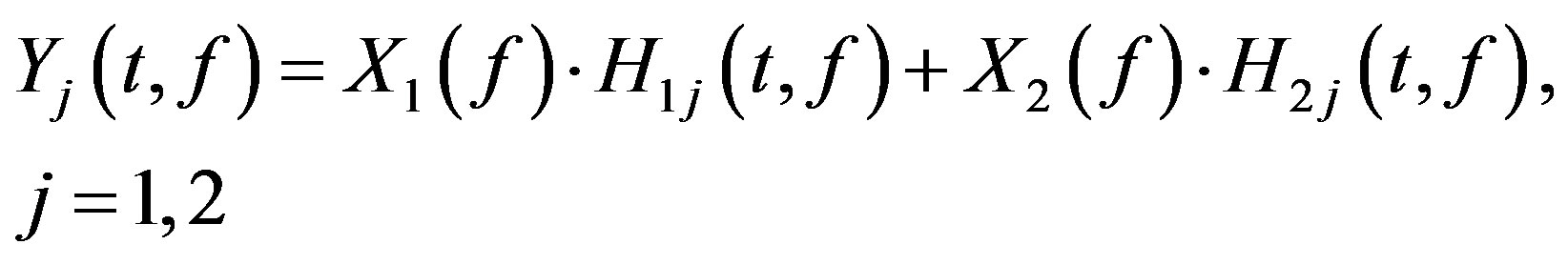 (2)
(2)
The development of the digital block of a channel hardware simulator requires a good knowledge of the propagation channel. The different models of channels presented in literature used to apprehend as faithfully as possible the behavior of the channel.
Two channel models are considered to cover indoor and outdoor environments: the TGn channel models (indoor) and the 3GPP-LTE channel models (outdoor). Moreover, using the channel sounder realized at IETR, measured impulse responses are obtained for specific environments: shipboard, outdoor-to-indoor.
2.1. TGn Channel Models
TGn channel models [27] have a set of 6 profiles, labeled A to F, which cover all the scenarios. Each model has a number of clusters. For example, model E has four clusters. Each cluster corresponds to specific tap delays, which overlaps each other in certain cases. Reference [27] summaries the relative power of the impulse responses for TGn channel model E by taking the LOS impulse response as reference. According to the standard (WLAN 802.11ac) and its bandwidth, the sampling frequency is fs = 165 MHz and the sampling period is Ts = 1/fs.
2.2. 3GPP-LTE Channel Models
3GPP-LTE channel models are used for mobile wireless applications. A set of 3 channel models is used to simulate the multipath fading propagation conditions. A detailed description is presented in [28]. For LTE signals, fs = 50 MHz.
2.3. Time-Varying Channels
In this section, we present the method used to obtain a model of a time variant channel, using Rayleigh fading [39] and based on Kronecker model [40]. The Doppler frequency fd is equal to:
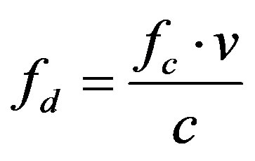 (3)
(3)
where c is the celerity and v is the environmental speed. We have chosen a refresh frequency fref > 2fd to respect the Nyquist-Shannon sampling theorem.
For an indoor environment (TGn model E for example), at fc = 5 GHz and v = 4 km/h, fd = 18.51 Hz. Thus, we have chosen fref = 40 Hz. For an outdoor environment (3GPP-LTE model EVA for example), at fc = 1.8 GHz and v = 80 km/h, fd = 133.27 Hz. Thus, we have chosen fref = 300 Hz.
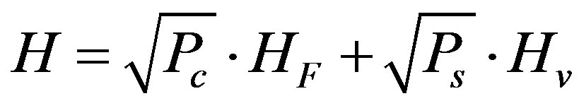
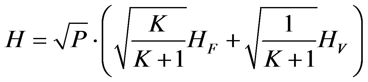
The MIMO channel matrix H can be characterized by two parameters:
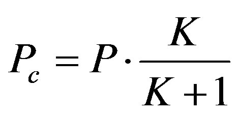
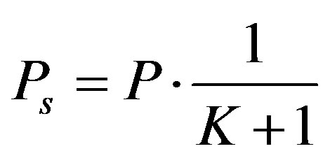
1) The relative power Pc of constant channel components which corresponds to the LOS. 2) The relative power Ps of the channel scattering components which corresponds to the Non-Line-Of-Sight (NLOS).The ratio Pc/Ps is called Ricean K-factor. Assuming that all the elements of the MIMO channel matrix H are Rice distributed, it can be expressed for each tap by:
 (4)
(4)
where HF and HV are the constant and the scattered channel matrices respectively.
The total relative received power P = Pc + Ps. Therefore:
 (5)
(5)
 (6)
(6)
If we combine (5) and (6) in (4) we obtain:
 (7)
(7)
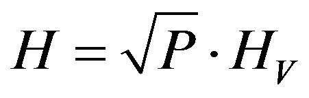
To obtain a Rayleigh fading channel, K is equal to zero, so H can be written as:
 (8)
(8)
P is derived from [27,28] for each tap of the considered impulse response. For 2 transmit and 2 receive antennas:
 (9)
(9)
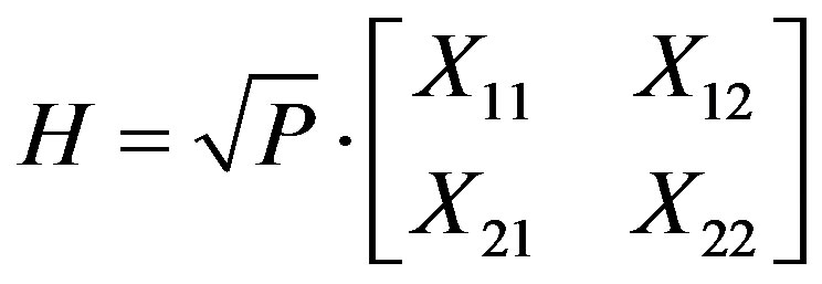
where Xij (i-th receiving and j-th transmitting antenna) are correlated zero-mean, unit variance, complex Gaussian random variables as coefficients of the variable NLOS (Rayleigh) matrix HV.
To obtain correlated Xij elements, a product-based model is used [40]. This model assumes that the correlation coefficients are independently derived at each end of the link:
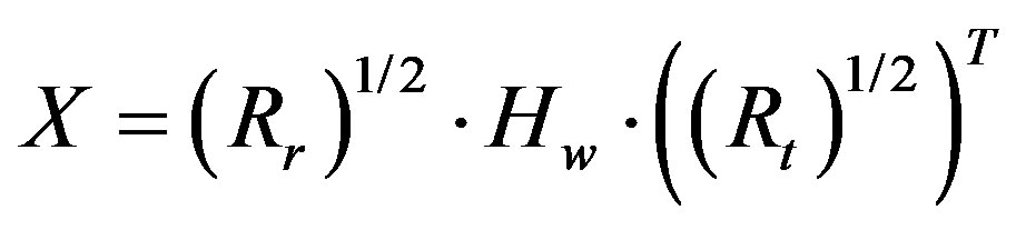 (10)
(10)
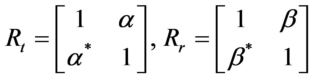
Hw is a matrix of independent zero means, unit variance, complex Gaussian random variables. Rr and Rt are the receive and transmit correlation matrices. They can be written by:
 (11)
(11)
where  is the correlation between channels at two receives antennas, but originating from the same transmit antenna (SIMO). In other words, it is the correlation between the received power of channels that have the same Angle of Departure (AoD).
  is the correlation coefficient between channels at two transmit antennas that have the same receive antenna (MISO).
The use of this model has two conditions:
1) The correlations between channels at two receive (resp. transmit) antennas are independent from the Rx (resp. Tx) antenna.
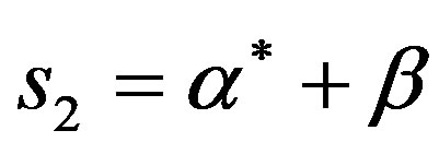
2) If s1, s2 are the cross-correlation between antennas of the same side of the link, then:
• 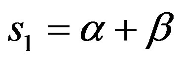 .
.
•  .
.
For the uniform linear array, the complex correlation coefficients  and
and  are expressed by
  :
:
 (12)
(12)
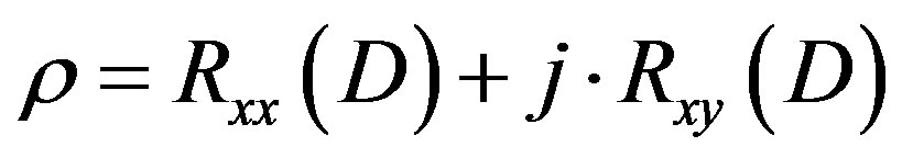
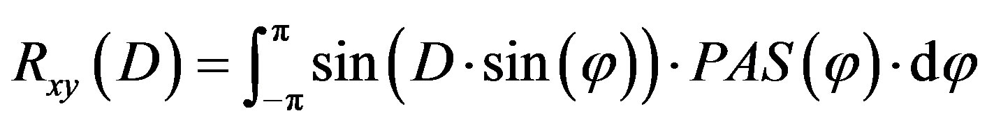
where D = 2πd/λ, d = 0.5λ is the distance between two successive antennas, λ is the wavelength and Rxx and Rxy are the real and imaginary parts of the cross-correlation function of the considered correlated angles:
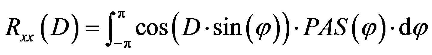 (13)
(13)
 (14)
(14)
The Power Angular Spectrum (PAS) closely matchs the Laplacian distribution [41,42]:
 (15)
(15)
where σ is the standard deviation of the PAS (which corresponds to the numerical value of AS).
3. Digital Block Architecture
In this section, the architecture of the digital block of the hardware simulator is presented. First, the simple time domain architecture is described, and then the ASF-based architecture is presented and analyzed.
3.1. Simple Time Domain Architecture
We simulate 2 × 2 MIMO channel. Therefore, four FIR filters are considered to present the four SISO channels. For each channel, the FIR width and the number of used multipliers are determined by the taps of each channel. 4 FIR filters with 18 multipliers each are considered. Figure 1 presents two SISO channels of the time domain architecture based on FIR 147 filter with 18 multipliers.
We have developed our own FIR filter instead of using Xilinx MAC FIR filter to make it possible to reload the FIR filter coefficients. The general formula for a FIR filter with 18 multipliers is:
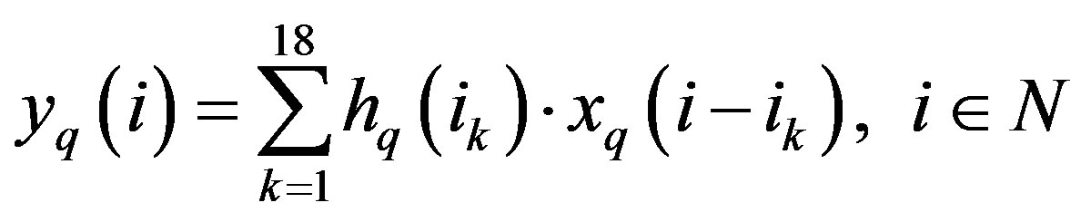 (16)
(16)
In this relation, the index q suggests the use of quantified samples and hq(ik) is the attenuation of the kth path with the delay ikTs.
The truncation block is located at the output of the final digital adder. It is necessary to reduce the number of bits to 14 bits. Thus, these samples can be accepted by the digital-to-analog converter (DAC), while maintaining the highest accuracy. The immediate solution is to keep the first 14 bits. It is a “brutal” truncation (BT). This truncation decreases the real value of the quantified output
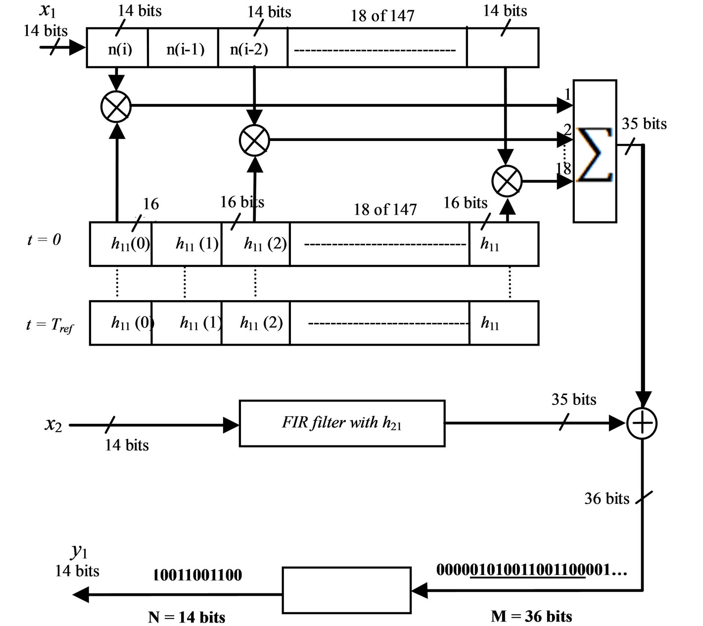
Figure 1. FIR 147 with 23 multipliers for one h11 and h21.
sample. Moreover, 36 − 14 = 22 bits will be eliminated. Thus, instead of an output sample y, we obtain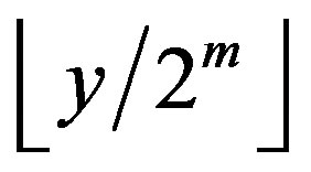 , where
  is the biggest integer number smaller or equal to u.
However, for low voltages, the brutal truncation generates zeros to the input of the DAC. Therefore, a better solution is the sliding truncation (ST) presented in Figure 1 which uses the 14 most significant bits. This solution modifies the output sample values. Therefore, the use of a reconfigurable amplifier after the DAC must be used to restore the correct output value. It must be divided by the corresponding sliding factor.
3.2. ASF-Based Time Domain Architecture
3.2.1. Why Using an ASF-Based Architecture?
To present the cause of using ASF-based time domain architecture, we related the input signals parameters and the relative power of the impulse responses to the relative error and SNR of the output signals. After analyzing the influence of these parameters on the output error and SNR, an improvement algorithm based on an Auto-Scale Factor ASF is proposed and analyzed in details.
In order to determine the accuracy of the digital block, a comparison is made between the theoretical/Xilinx output signals. An input Gaussian signal x(t) is considered for the two inputs of the 2 × 2 MIMO simulator. To simplify the calculation, we consider x(t) = x1(t) = x2(t):
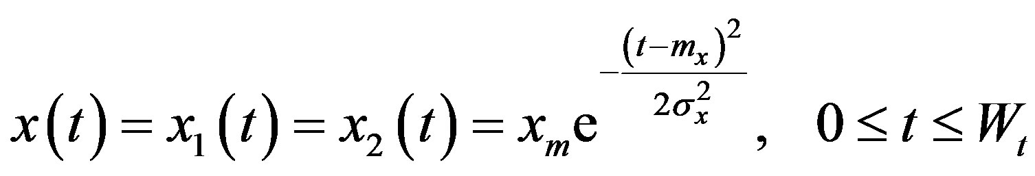 (17)
(17)
In fact, the FT of a Gaussian signal is also Gaussian signal, and to obtain a signal x(t) that respect the bandwidth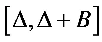 , the following steps are considered:
In frequency domain, the Gaussian input signal  is computed by:
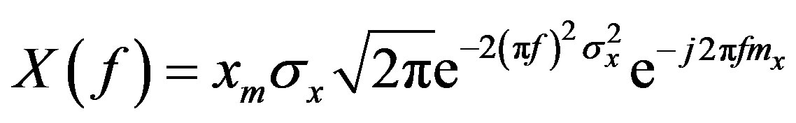 (18)
(18)
with
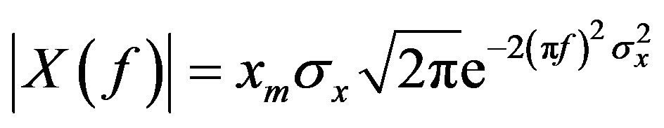 (19)
(19)
This signal spectrum is limited between  and
and 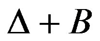 if:
if:
 (20)
(20)
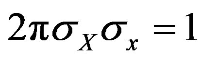
where  is the standard deviation of
 . Comparing the first and the third equation, we obtain:
 (21)
(21)
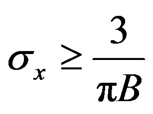
Thus,  that corresponds to the considered band of the standard used, is obtained:
 (22)
(22)
To obtain x(t) centered between , it must be multiplied by:
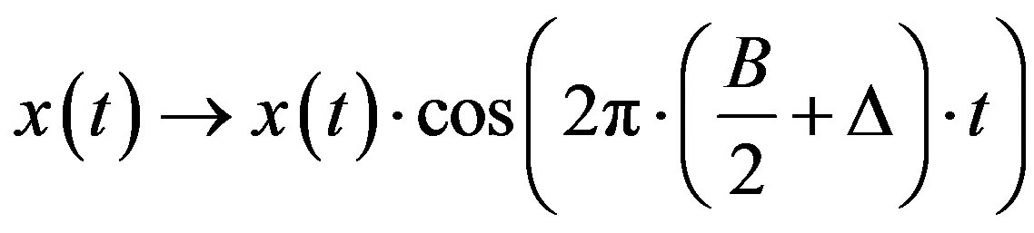 (23)
(23)
In our work, we considered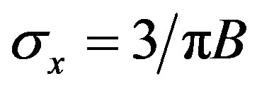 . mx is chosen equal to
 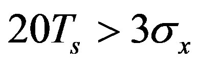 for both WLAN 802.11ac and LTE signals. Moreover,
  is chosen equal 2 MHz. These values are small enough to show the effect of each tap on the output signal. The ADC and DAC converters of the development board have a full scale [−Vm,Vm]with Vm = 1 V. For the simulations, we consider xm = Vm/2.
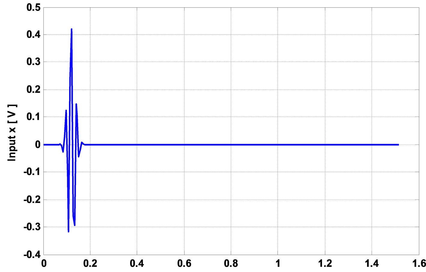
For WLAN 802.11ac, B = 80 MHz and Ts = 1/fs = 6 ns. Thus, we obtain 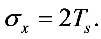 This signal is named xWLAN(t) and is presented in Figure 2.
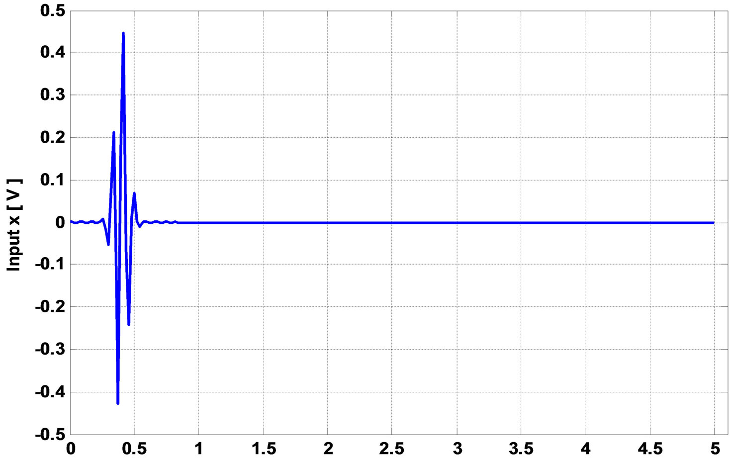
For LTE, B = 20 MHz and Ts = 1/fs = 20 ns. Thus, we obtain  = 2.5Ts. This signal is named xLTE(t) and is presented in Figure 3.
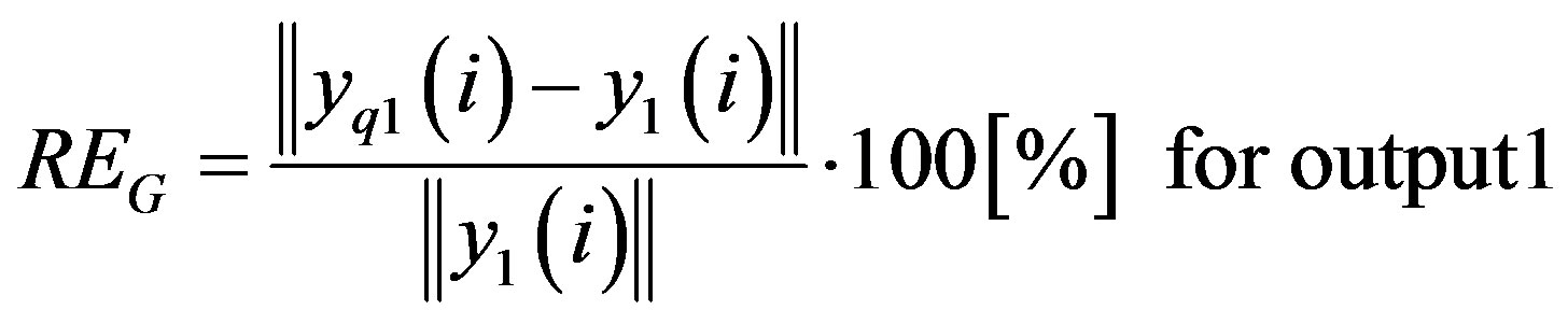
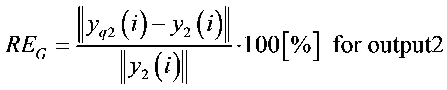
The global output SNR can be affected by the input signal and the impulse response. The output global SNR of the first output is calculated by:
 Time [μs]
Figure 2. Input signal for WLAN 802.11ac for the 2 × 2 time domain architecture.
 Time [μs]
Figure 3. Input signal for LTE for the 2 × 2 time domain architecture.
 (24)
(24)
and for the second output by:
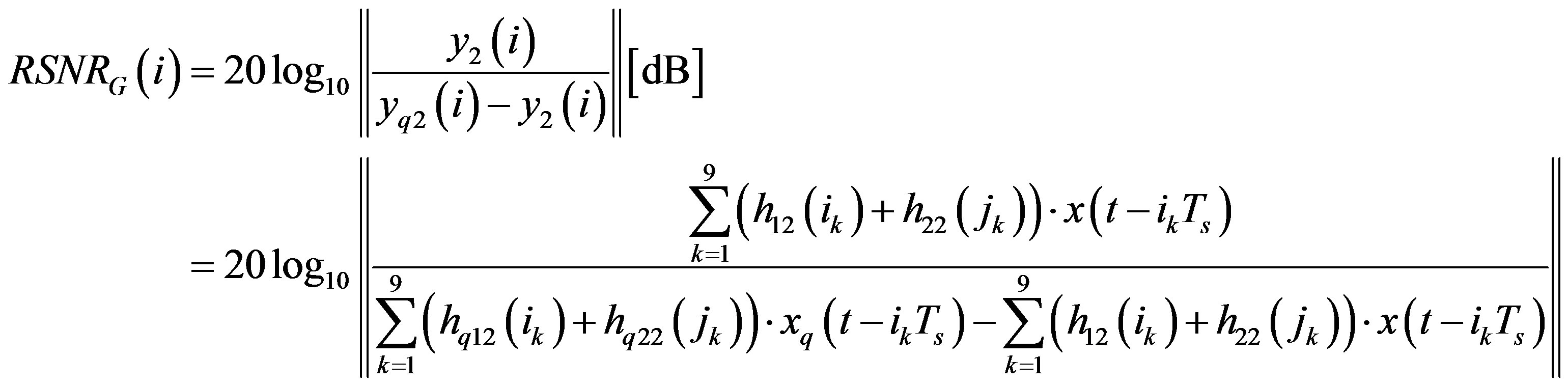 (25)
(25)
where hq and xq are the quantified impulse responses and input signal respectively.
The parameters of the input signal that have an impact on the output global SNR are: xm,  , Wt and nx, where nx is the number of bits of the input signal. However, nx is fixed by the ADC by 14 bits. Thus, it won’t be considered in the study.
If xm decreases, then  decreases. Thus, x will be quantified on lower number of bits. Therefore, the global SNR decreases. Figure 4 presents the global output SNR versus xm for the TGn model E and for 3GPP-LTE model EVA respectively.
If  decreases, then more samples of the input signal x will be quantified on lower number of bits. Therefore, the global SNR decreases. The amount of the low values of x is related to
  and Wt.
Figure 5 presents the global output SNR versus  for the TGn model E and for 3GPP-LTE model EVA respectively.
After a simple calculation, we notice that  and Wt are linear related, as presented in Figure 6.
Thus, we define a factor  equal to the null part of x:
 (26)
(26)
If Wt increases or/and  decreases, Fx increases which leads to a large interval of small values of x. Thus, the global SNR decreases. Figure 7 presents the global output SNR versus Fx.
The number of bits of the impulse response (h) has an impact on the output SNR. In fact, quantifying h on lower number of bits decreases the global output SNR. Figure 8 presents the output global SNR versus nh, where nh is the number of bits of h.
3.2.2. ASF-Based Architecture Description
After analyzing the global relative SNR, we conclude that it is high only for high values of the input signals
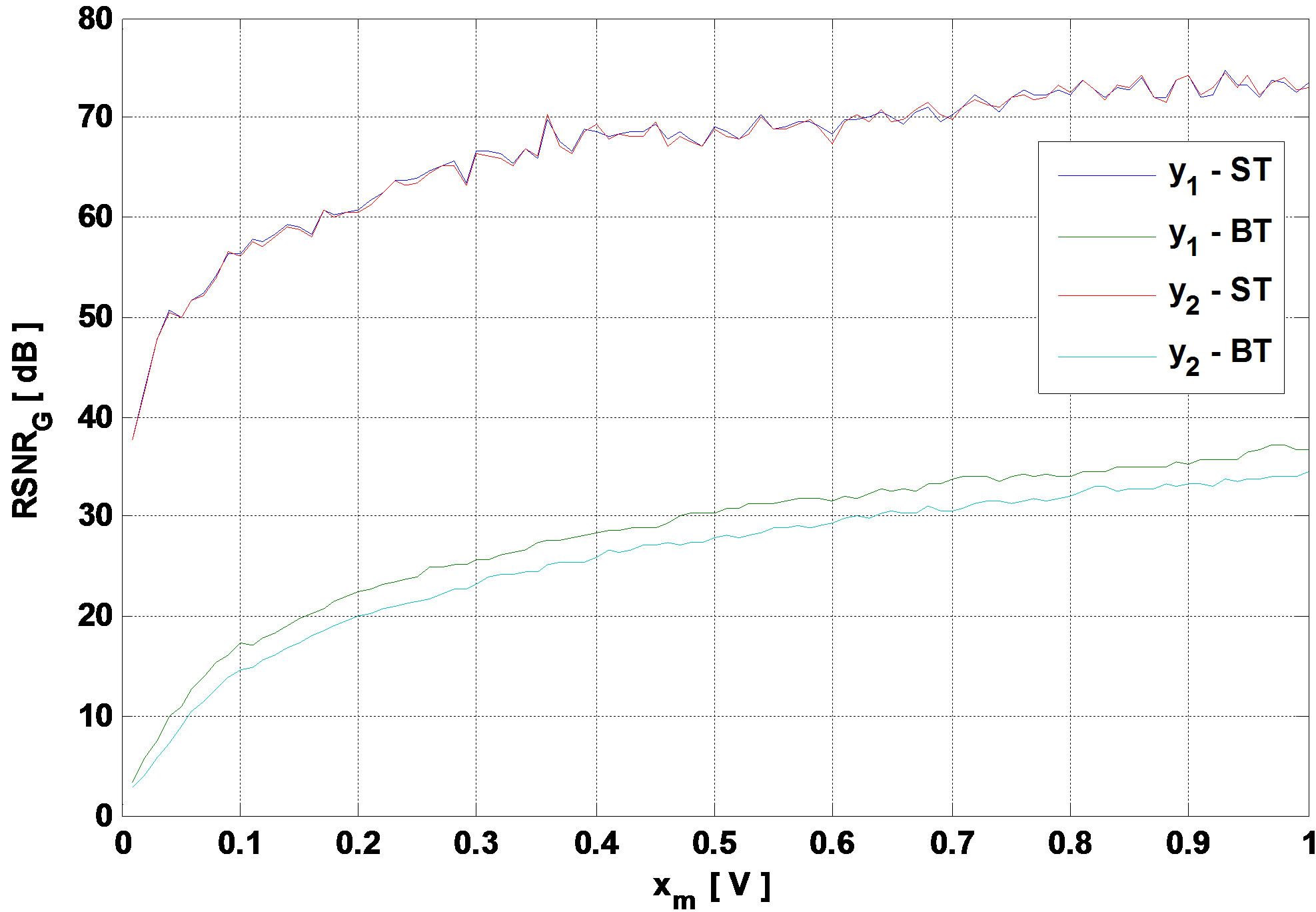
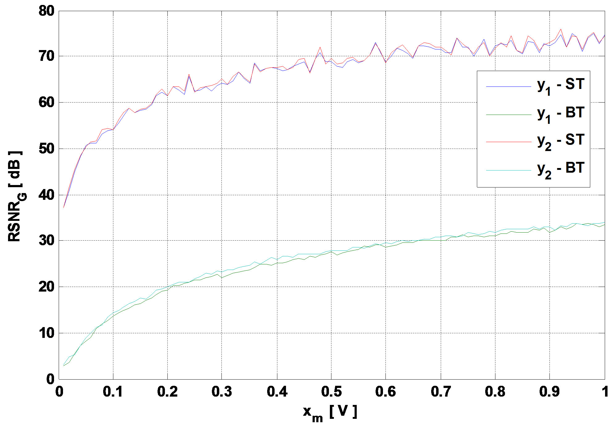
Figure 4. Global SNR versus xm for TGn model E and 3GPP-LTE model EVA respectively.
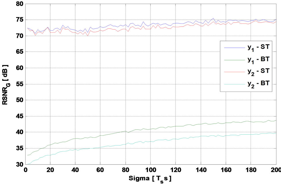
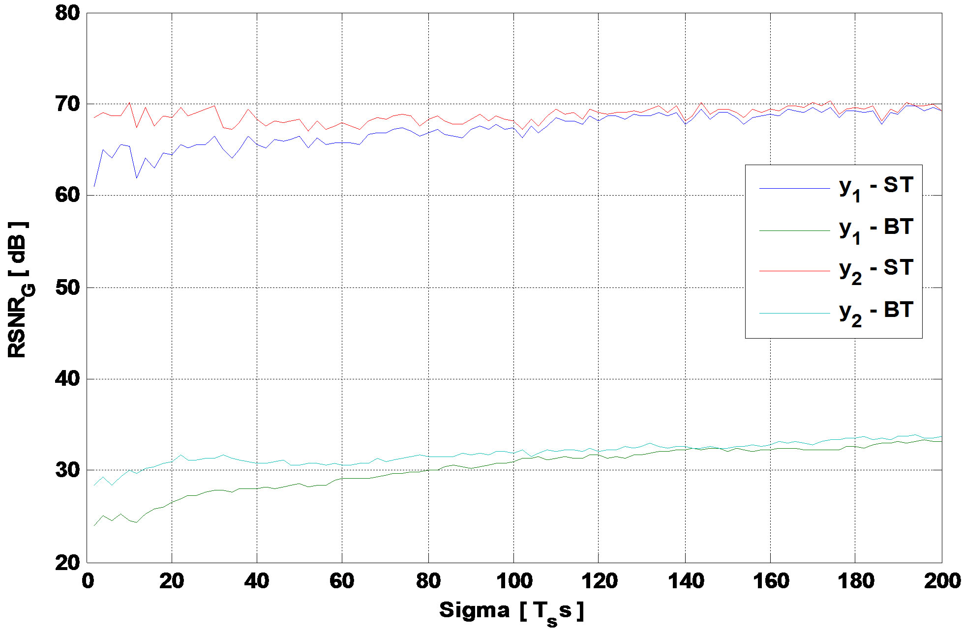
Figure 5. Global SNR versus σ for TGn model E and 3GPP-LTE model EVA respectively.
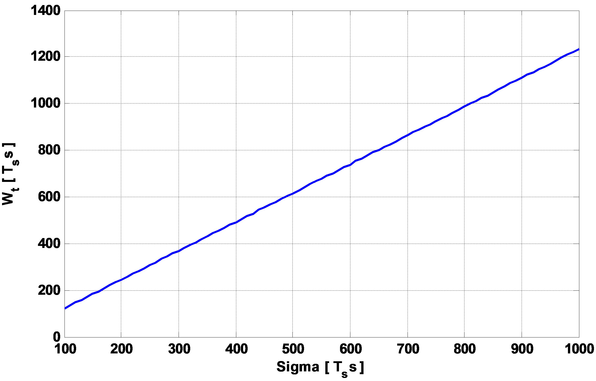
Figure 6. Wt versus σ for the input signal.
Figure 7. Global output SNR versus Fx for TGn model E and 3GPP-LTE model EVA respectively.
and the impulse response. Therefore, to decrease the error at the simulator output signals, it is better to consider a large number of bits in the architecture for the input signals and for the impulse response.
In the context of mobile radio, the input signals and the impulse response cannot be predicted and they can undergo fading and be strongly attenuated. If the signal is low, it will not be quantified on a sufficient number of bits. Thus, the error of the output signals of the channel simulator will increase widely. The proposed solution consists on multiplying the input signals and the impulse response by an ASF that increases the output signals and makes it possible to quantify them on a higher number of bits in order to decrease the error at the output. Moreover, the received signal is divided by the correct ASF to obtain the correct output.
Figure 9 presents the global ASF diagram. This diagram will be described and analyzed in details. The new 2 × 2 MIMO ASF-based architecture is presented in Figure 10.
The two signals x1(t) and x2(t) are the input signals of the 2 × 2 MIMO channel, and the two signals y1(t) and y2(t) are the output signals.
The colored large block is the programmable digital part (Virtex-IV) of the hardware simulator. “I” stands for Input and “O” for Output.
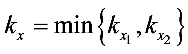
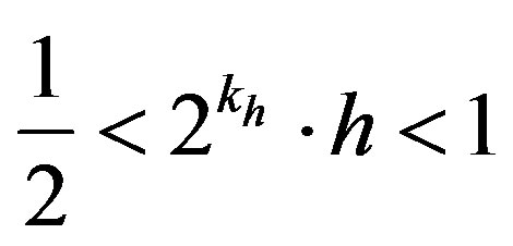
The maximum voltage supported by the ADC is 1 V. If x1 < 0.25 V, it is multiplied by  where
where  is the integer verifying:
 (27)
(27)
with
 (28)
(28)
In the same way, If x2 < 0.25 V, it is multiplied by  where
where  is the integer verifying:
 (29)
(29)
with
 (30)
(30)
The input signal cannot exceed 1 V. Thus, we define  by:
by:
 (31)
(31)
In fact, we cannot provide the digital input by the signals  and
and . Otherwise, the ASF calculated and provided to the digital output will be unknown.
If , it is multiplied by
 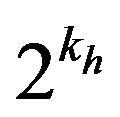 where:
 (32)
(32)
with
 (33)
(33)
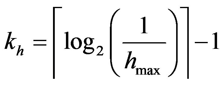
kh is determined for every MIMO profile and it is saved in a RAM block in the FPGA. A gain controlled amplifier is placed before the ADC to control the input
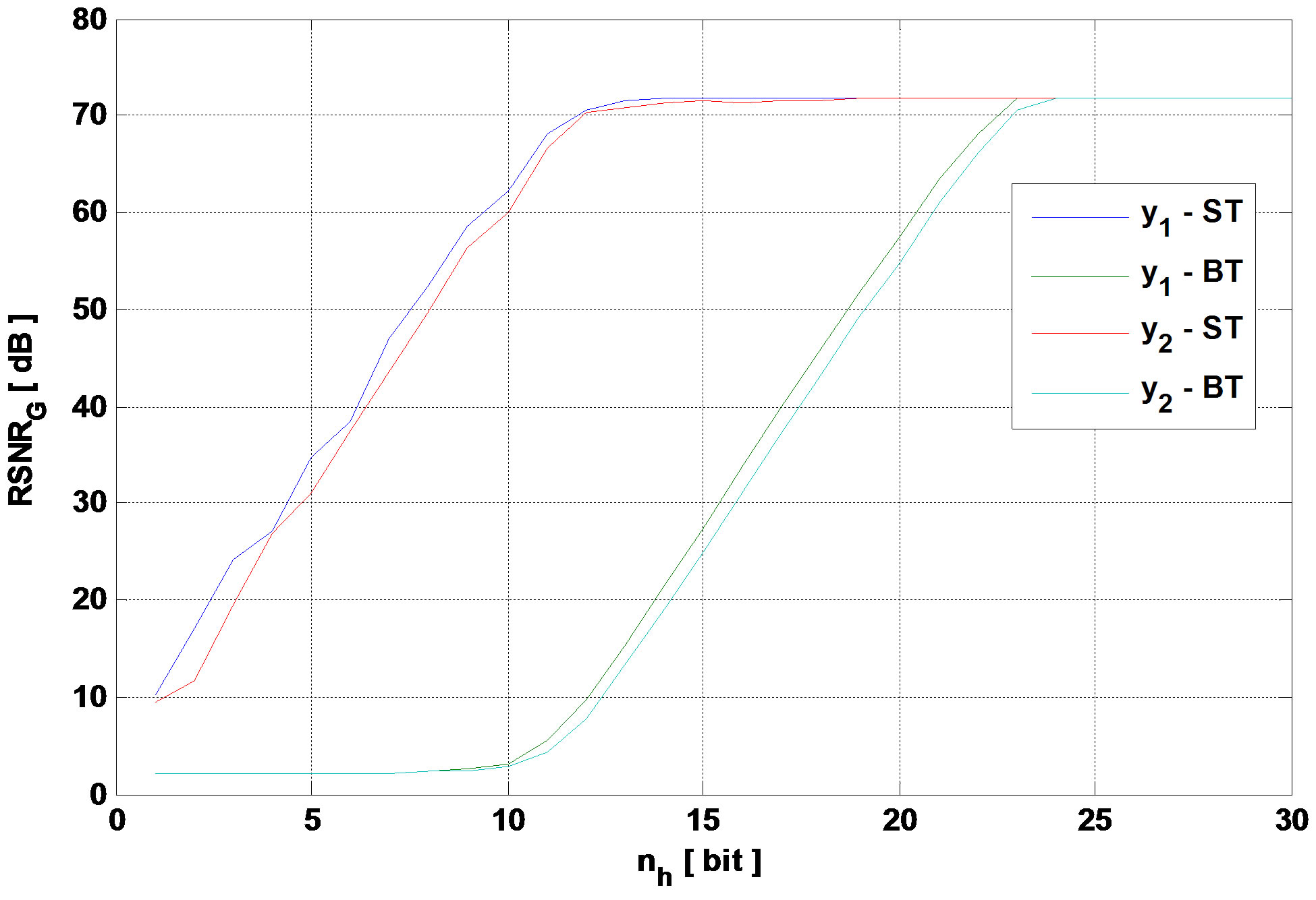
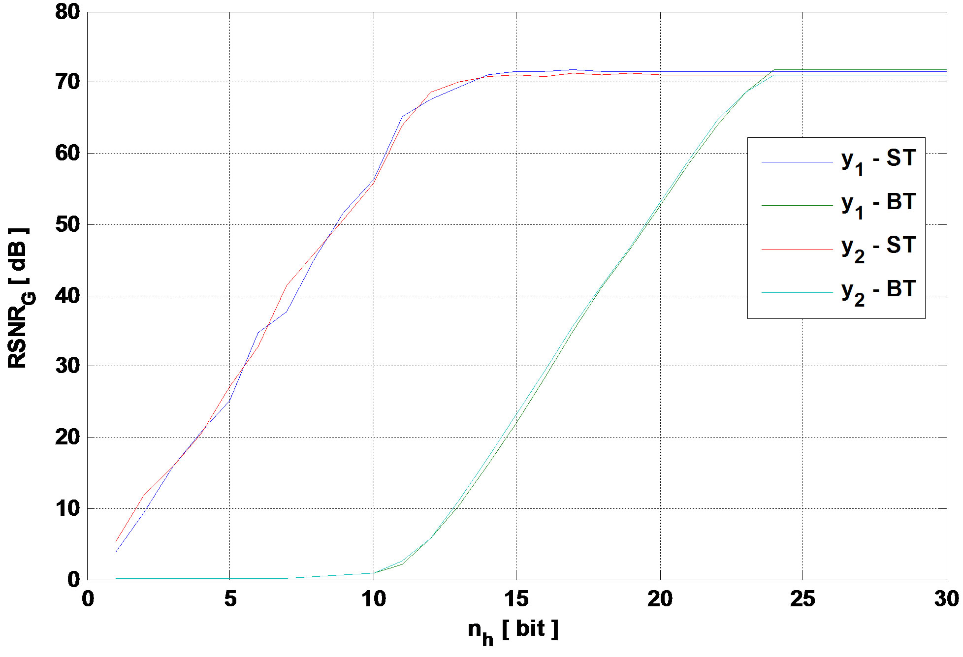
Figure 8. Global output SNR versus nh for TGn model E and 3GPP-LTE model EVA respectively.
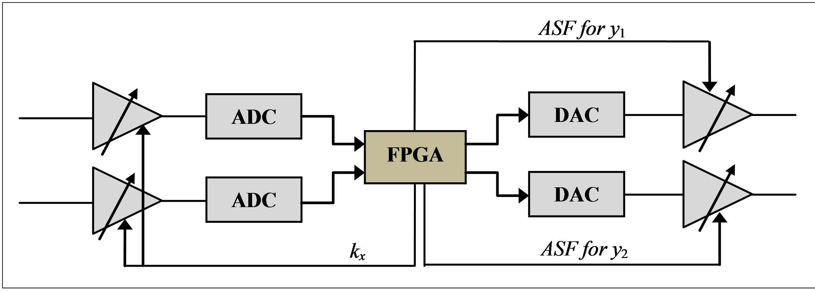
Figure 9. ASF diagram using the gain controlled amplifiers.
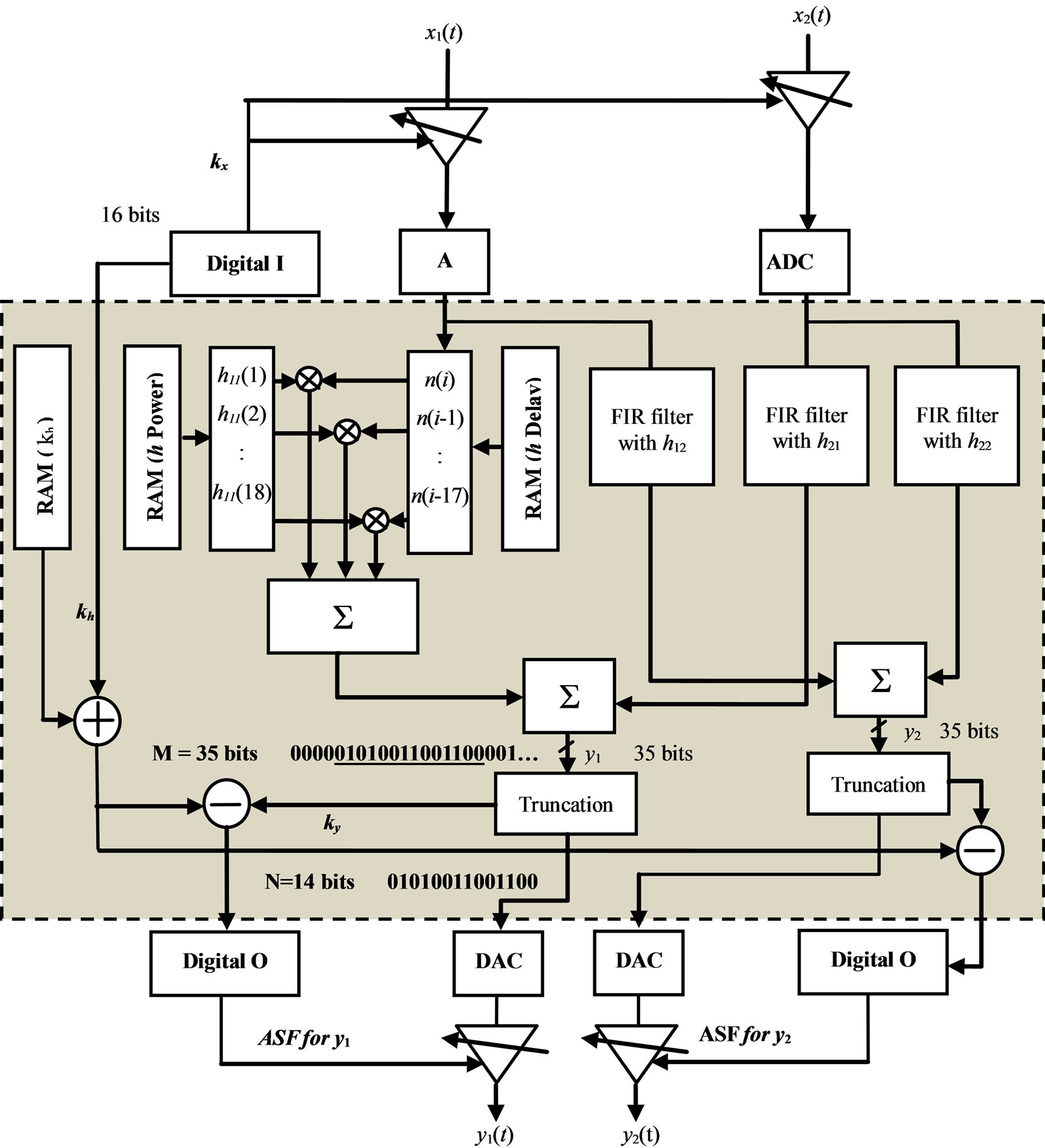
Figure 10. Principle scheme using ASF.
signals by  before sending it to the FPGA. Also, controlling the power of the input signal at a sampling period smaller than the sampling period of the FPGA is not easy (or realistic). Thus,
  is provided for a package of input samples.
Figure 11 describes the electronic ship that we developed to control the input signals by . The figure present one control amplifier for one input signal. U is the initial power of the input signal and R are resistances.
In the case of a brutal truncation, 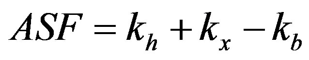
where  is the fixed brutal truncation equal to 235−14 = 221 (35 bits for the output before truncation and 14 bits for the output after truncation). Moreover, a better solution is the sliding truncation, described previously, that selects the most significant bits. The ADC and the DAC
have a resolution of 14 bits. In this case, if the output signals are presented on more than 14 bits, the sliding factor  has to be considered to obtain the correct output signal. Thus,
  , and using just the ASF on h,
 . The resulting ASF is sent to a gain controlled amplifier to restore the true value of the output signals, as presented in the figure of the global diagram of the ASF. The first MSB bit defines the multiplication or the division by 2ASF.
A FPGA Virtex-IV provides 34 pins (digital I/O) Adjacent Bus Header on the motherboard of the FPGA. This will provides 28 direct bi-directional connections to the main user FPGA. The remainder of the pins provides a 3.3 V connection, a GND connection and they are No-Connects (NC). Thus, kx provided to the input of the
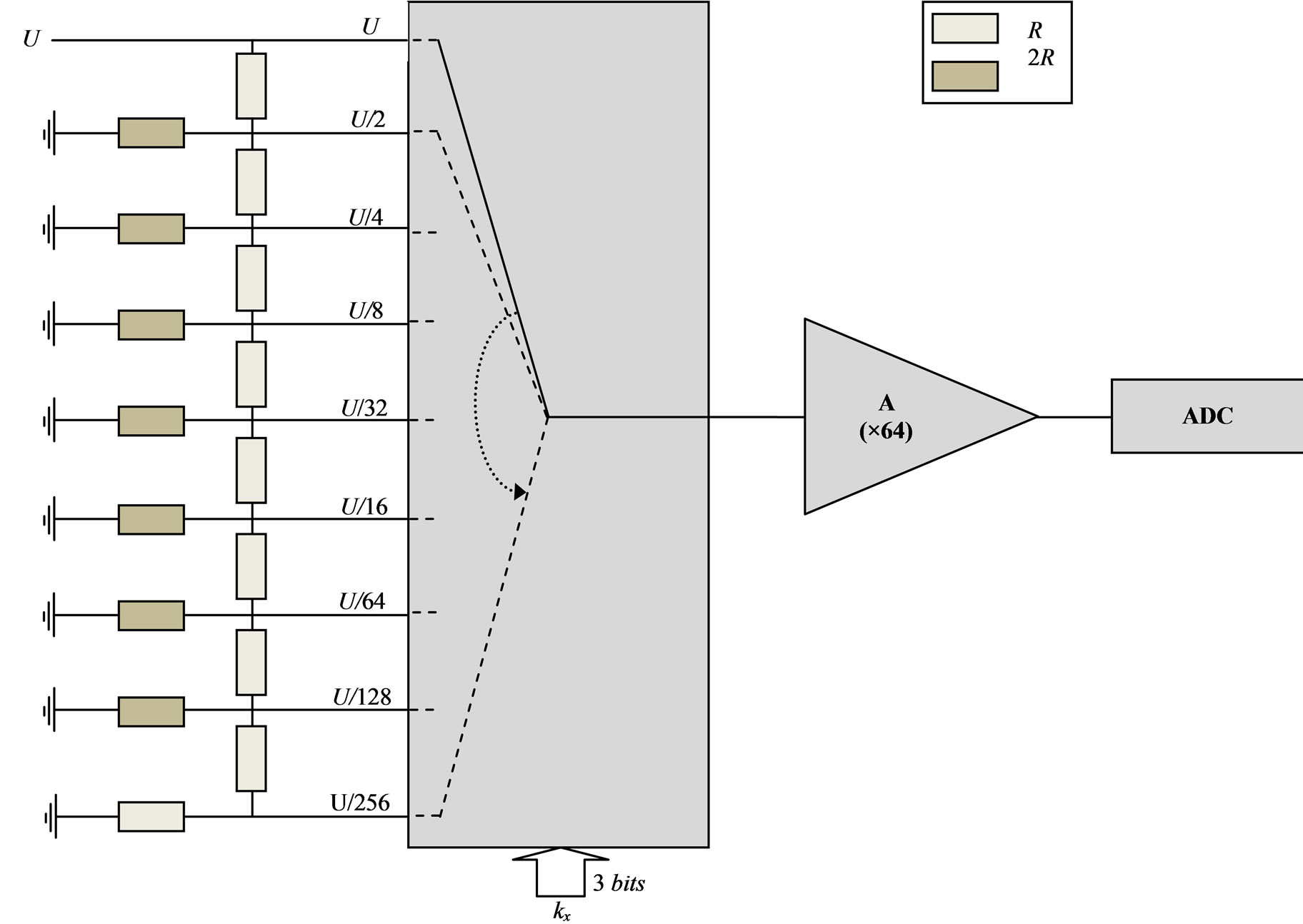
Figure 11. Electronic ship to control the input signal.
FPGA and the two ASF provided to the outputs y1 and y2 are quantified on 9 bits. In fact, as presented in the previous figure, 3 bits for the quantification is sufficient for this work. The input (output resp.) signal can be multiplied (divided resp.) by  which is about 25 dB. Higher than 25 dB, the noise undergoes the ASF process and it will grow significantly.
4. Accuracy Evaluation
4.1. Occupation on FPGA
The Xtreme DSP Virtex-IV board from Xilinx [33] is used for the implementation. The XtremeDSP features dual-channel high performance ADCs (AD6645) and DACs (AD9772A) with 14-bit resolution, a user programmable Virtex-IV FPGA, programmable clocks, support for external clock, host interfacing PCI, two banks of ZBT-SRAM, and JTAG interfaces. The simulations and synthesis are made with Xilinx ISE [33] and ModelSim software [43].
The 2 × 2 MIMO architectures are implemented in the FPGA Virtex-IV which has 2 ADC and 2 DAC, it can be connected to only 2 down-conversion and 2 up conversion RF units. To test a higher order MIMO array, the use of more performing FPGA as Virtex-VII [33] is recommended.
In the FPGA, the clock is controlled by a Virtex-II which is connected to the Virtex-IV.
As the development board has 2 ADC and 2 DAC, it can be connected to only 2 down-conversion and 2 upconversion RF units. Four FIR filters are needed to simulate a one-way 2 × 2 MIMO radio channel. The occupancy of the time domain architecture is known after performing operations of synthesis, mapping, place and route from the program written in VHDL.
Table 1 shows the device utilization in one Virtex-IV SX35 for 2 × 2 MIMO channel using the time domain architecture for the TGn channel model E, with their additional circuits used to dynamically reload the channel coefficients.
Table 2 shows the device utilization in one Virtex-IV SX35 for 2 × 2 MIMO channel using the time domain architecture for the 3GPP-LTE model EVA.
We notice that the occupation of slice on the FPGA of a 2 × 2 MIMO system is 16% for the TGn channel model E and 16% for the 3GPP-LTE model EVA. In fact, these occupations are equal to the occupations of a SISO channel multiplied by four and with additional slices added because of the two digital adders that operates y11 + y21 and y12 + y22. Moreover, the 2 × 2 MIMO system has small occupation on the FPGA Virtex-IV. In fact, we can implement up to 4×4 MIMO system in the FPGA for
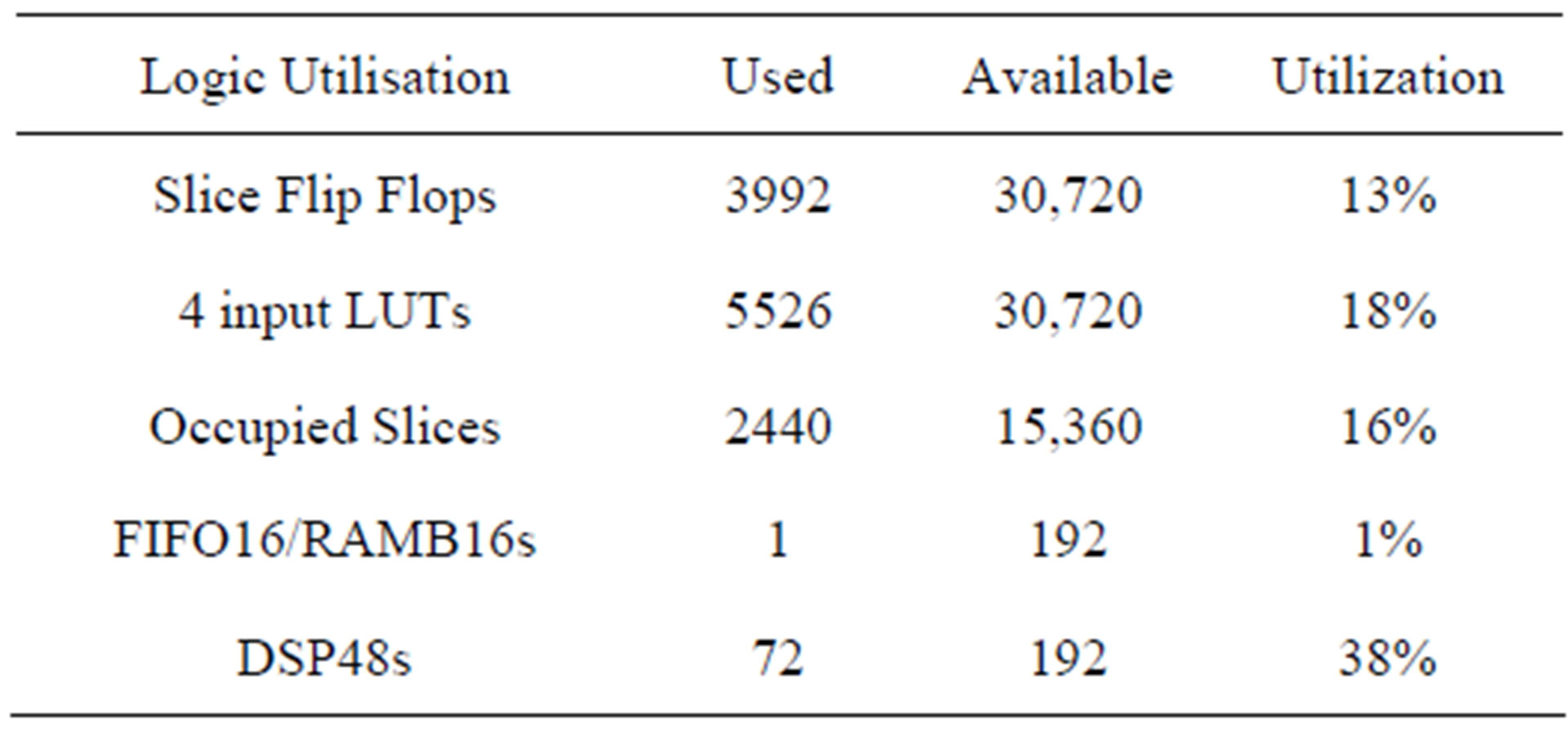
Table 1. Virtex-IV utilization summary for the 2 × 2 MIMO simple time domain architecture, for TGn model E.
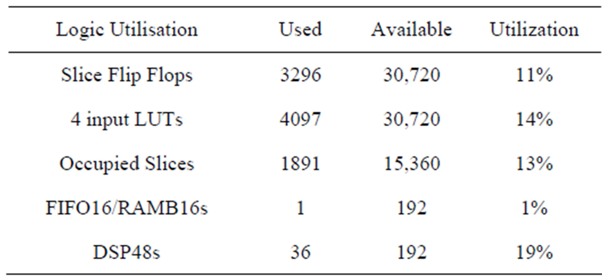
Table 2. Virtex-IV utilization summary for the 2 × 2 MIMO simple time domain architecture, for 3GPP-LTE model EVA.
the 3GPP-LTE model EVA (because for TGn channel model E the number of multiplier is equal to 18 × (4 × 4) = 288 >192). However, we are limited by the 2 ADC and the 2 DAC.
Table 3 shows the device utilization in one Virtex-IV SX35, after performing operations of synthesis, mapping, place and route, for 2 × 2 MIMO channel using the ASF-based time domain architecture for the TGn channel model E.
Table 4 shows the device utilization in one Virtex-IV SX35 for 2 × 2 MIMO channel using the ASF-based time domain architecture for the 3GPP-LTE model EVA.
We notice that the occupation of slice on the FPGA using the ASF-based architecture increases about just 1%. However, as we will see in the next section, the precision of the output signals increase significantly.
The channel impulse responses are stored on the hard disk of the computer and read via the PCI bus and then stored in the FPGA dual-port RAM. Figure 12 shows the connection between the computer and the FPGA board to reload the coefficients. The successive profiles are considered for the test of a 2 × 2 MIMO time-varying channel.
The maximum data transfer of the impulse responses is: 18 × 4 = 72 words of 16 bits = 162 bytes to transmit for a MIMO profile, which is: 162 × fref(Bps). fref depends on the environment.
The MIMO profiles are stored in a text file on the hard disk of a computer. This file is then read to load the memory block which will supply RAM blocks on the
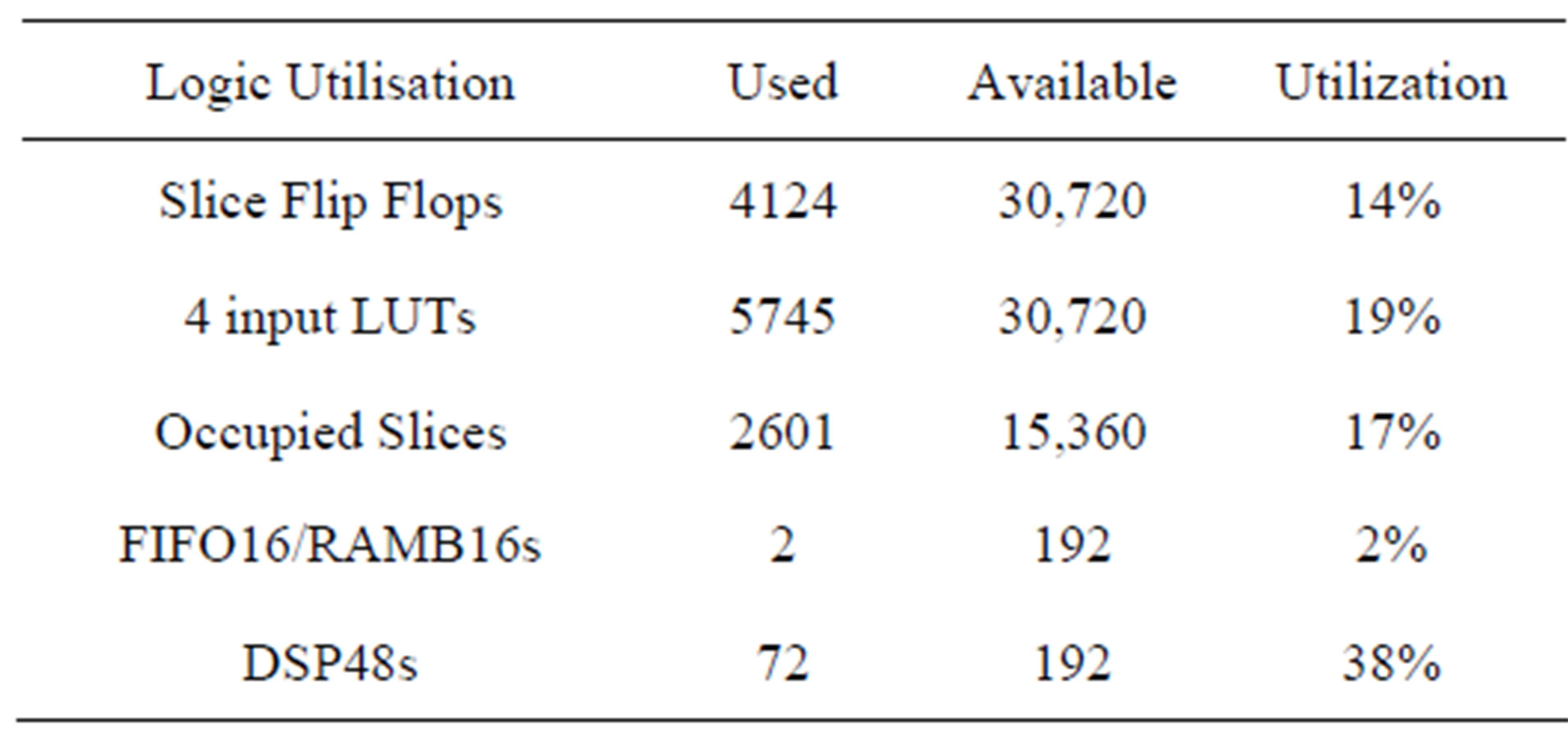
Table 3. Virtex-IV utilization summary for the 2 × 2 MIMO ASF-based time domain architecture, for TGn model E.
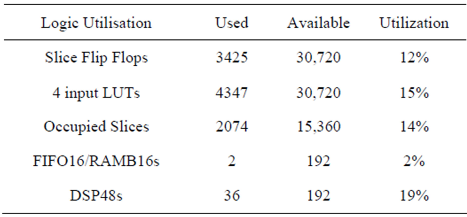
Table 4. Virtex-IV utilization summary for the 2 × 2 MIMO ASF-based time domain architecture, for 3GPP-LTE model EVA.
simulator (one block for each tap of the impulse response). Each block RAM has a memory of 64 (kB), thus 512 (kbits). The impulse responses are quantified on 16 bits, therefore, up to 32,000 MIMO profiles can be supplied in the RAM blocks. Each environment needs 4 blocks RAM for the power of the impulse responses and 4 blocks for the delays, which is a total of 8 blocks RAM. Reading the file can be done either from USB or PCI interfaces, both available on the used prototyping board. The PCI bus is chosen to load the profiles. It has a speed of 30 (MB/s). In addition, this is a bus of 32 (bits). Thus, on each clock pulse two samples of the impulse response are transmitted.
The Nallatech driver in Figure 12 provides an IP sent directly to the “Host Interface” that reads it from the PCI bus and stores these data in a FIFO memory. The module called “Loading profiles” reads and distributes the impulse responses in “RAM” blocks. While a MIMO profile is used, the following profile is loaded and will be used after the refresh period.
4.2. Output Signal Precision
In order to determine the accuracy of the digital block, a comparison is made between the theoretical and the Xilinx output signals.
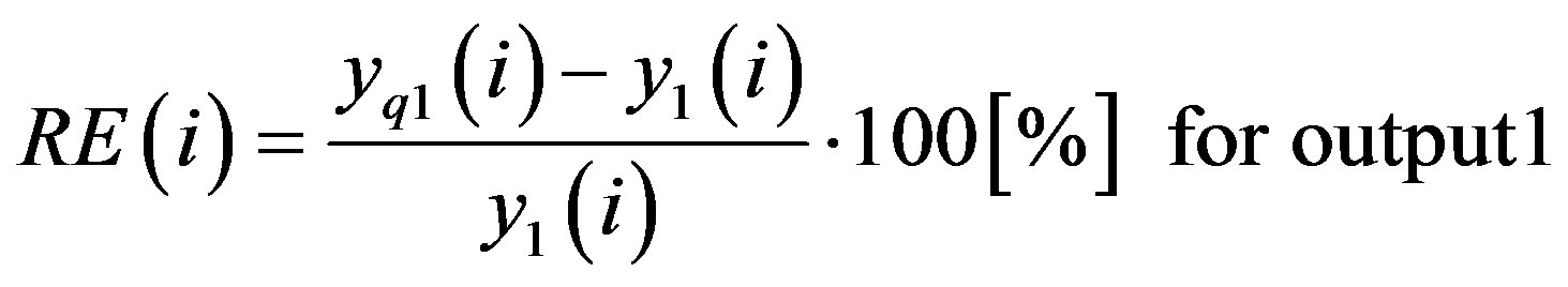
The theoretic output vector of the 2 × 2 MIMO channel is given previously. The relative error, which is given for each output sample, is calculated for the two outputs by:

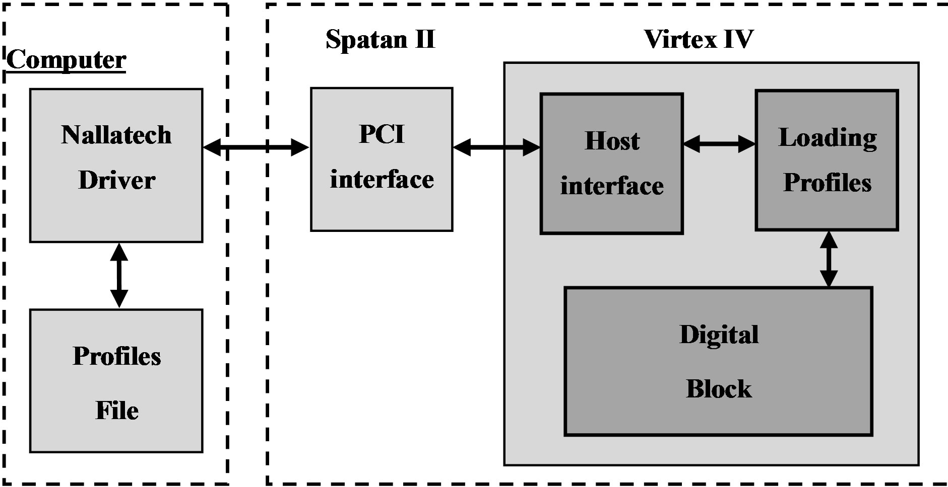
Figure 12. Connection between the computer and the XtremeDSP board.
 (34)
(34)
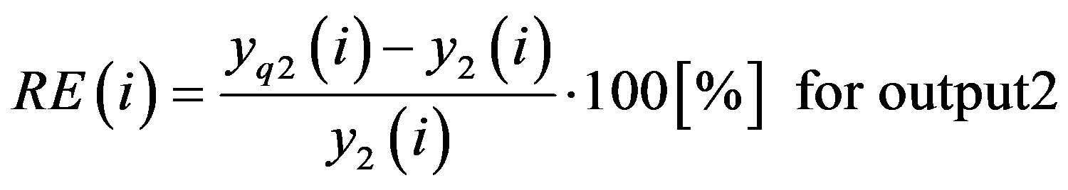 (35)
(35)
where yq1 and yq2 is the vector containing the samples of the Xilinx output signals, and y1 and y2 are the theory output signals.  and
and  is computed by for the two outputs by:
 (36)
(36)
 (37)
(37)
where imax11 = the index of the last tap ≠ 0 of h11
imax21 = the index of the last tap ≠ 0 of h21
imax12 = the index of the last tap ≠ 0 of h12
imax22 = the index of the last tap ≠ 0 of h22
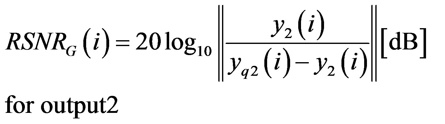
The relative SNR is computed for the two outputs by:
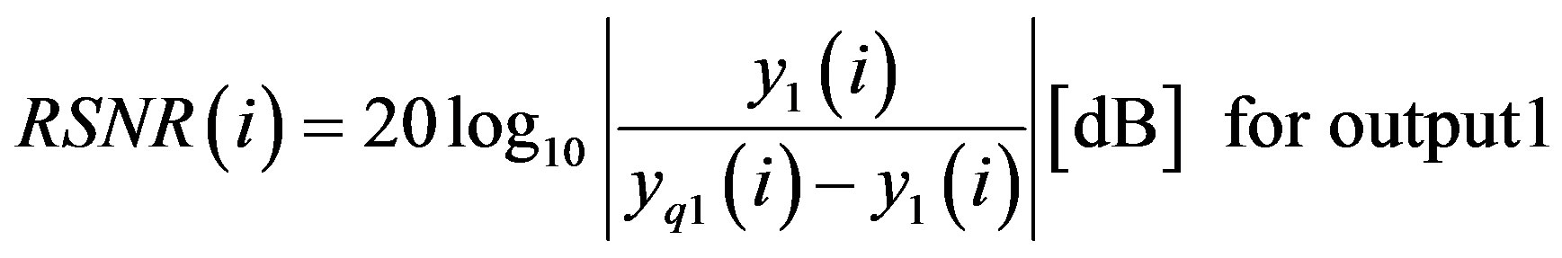 (38)
(38)
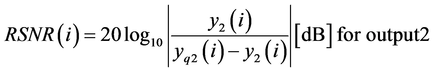 (39)
(39)
The global values of the relative error and SNR computed for the output signals after the final truncations are necessary to evaluate the accuracy of the architecture. The global relative error is computed for the two outputs by:
 (40)
(40)
 (41)
(41)
The global SNR is computed by:
 (42)
(42)
 (43)
(43)
Figure 13 presents the effect of the ASF on the global output SNR versus the attenuation of the impulse response h using TGn channel model E. Figure 14 presents the variation of  and
and 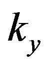 versus the attenuation of h using TGn channel model E.
Figure 15 presents the effect of the ASF on the global output SNR versus the attenuation of h using 3GPP-LTE channel model EVA. Figure 16 presents the variation of  and
and  versus the attenuation of h using 3GPP-LTE channel model EVA.
Using all the coefficient of ASF, the output global SNR achieve 100 dB and it remains above 97 dB for high attenuation of h. Moreover, 80 dB is considered as a high accuracy. Thus, the number of bits in the architecture can be decreased to obtain an output global SNR of 80 dB and a lower occupation on the FPGA to simulate higher order MIMO channels. Also, the result shows the benefit of the ST on the BT.
Table 5 presents the new values of the global output SNR before and after using ASF.
We notice that after adding ASF, the global output SNR increases significantly.
5. Conclusions
In this paper, the input signals parameters and the relative power of the impulse responses has been related to the relative error and SNR of the output signals. After analyzing the influence of these parameters on the output error and SNR, an improvement algorithm based on an Auto-Scale Factor (ASF) has been proposed and analyzed in details. In the context of mobile radio, the input signal and the impulse responses cannot be predicted and they can undergo fading and be strongly attenuated. Thus, the error of the output signals of the channel simulator will increase widely. The proposed solution consists on
Figure 13. ASF impact on global SNR versus the attenuation of h using TGn model E.
Figure 14. ASF parameters impact versus the attenuation of h using TGn model E.
Figure 15. ASF impact on global SNR versus the attenuation of h using 3GPP-LTE model EVA.
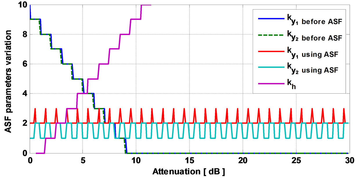
Figure 16. ASF parameters impact versus the attenuation of h using 3GPP-LTE model EVA.
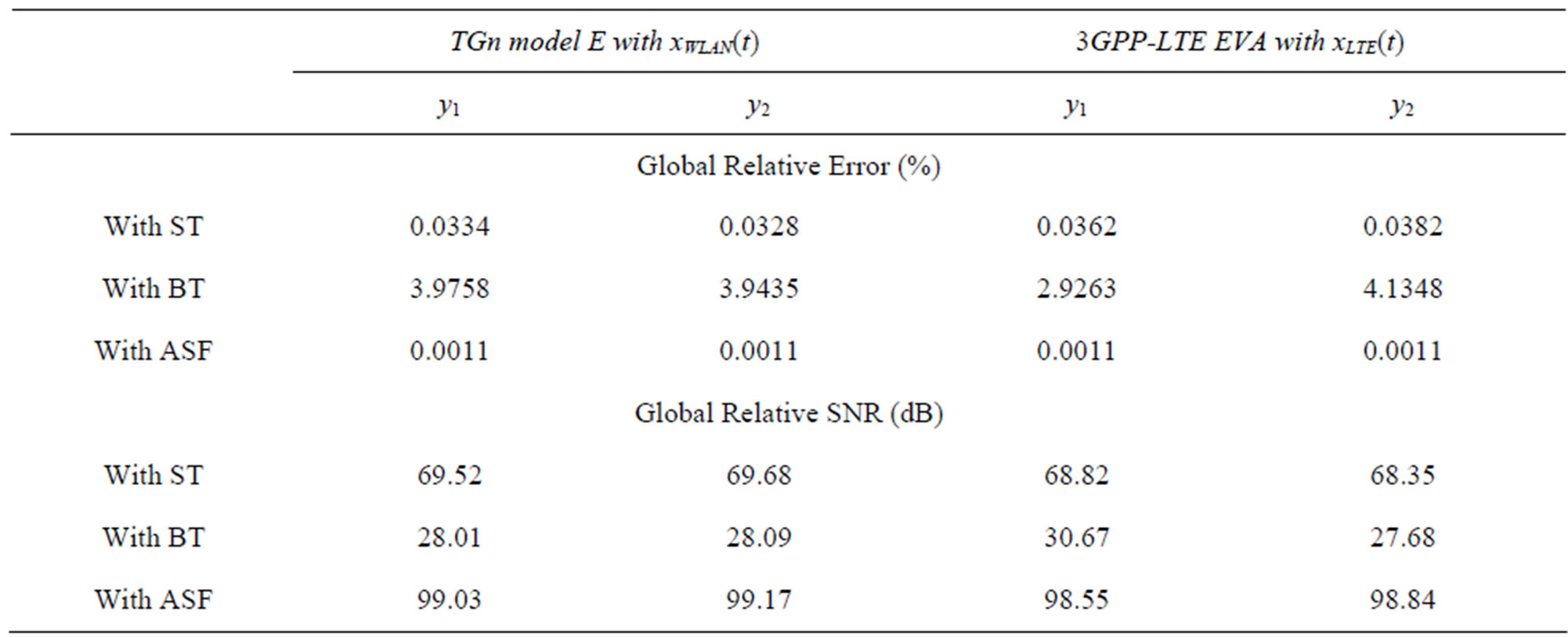
Table 5. Global relative error and SNR, for 2 × 2 MIMO ASF-based time domain architecture.
multiplying the input signal and the impulse responses by an ASF that increases the output signals and makes it possible to quantify them on a higher number of bits in order to decrease the error at the output. Moreover, the received signal is divided by the correct ASF to obtain the correct output. The new ASF-based architecture has been presented, designed and tested.
For our future work, simulations made using a Virtex-VII [33] XC7V2000T platform will allow us to simulate up to 300 SISO channels. In parallel, measurement campaigns will be carried out with the MIMO channel sounder realized by IETR to obtain the impulse responses of the channel for various types of environments. The final objective of these measurements is to obtain realistic MIMO channel models in order to supply the hardware simulator. A graphical user interface will also be designed to allow the user to reconfigure the simulator parameters.
6. Acknowledgements
This work is a part of CEDRE program and PALMYRE-II project with the support of “Region Bretagne”.
REFERENCES
- A. A. Gaston and W. H. Chriss, “A Multipath Fading Simulator for Mobile Radio,” IEEE Transaction on Vehicular Technology, Vol. 22, No. 4, 1973, pp. 241-244. doi:10.1109/T-VT.1973.23560
- R. Fitting, “Wideband Troposcatter Radio Channel Simulator,” IEEE Transaction Communication Technology, Vol. 15, No. 4, 1975, pp. 565-570. doi:10.1109/TCOM.1967.1089626
- J. R. Ball, “A Real-Time Fading Simulator for Mobile Radio,” Radio and Electronic Engineer, Vol. 52, No. 10, 1982, pp. 475-478.
- M. Lecours and F. Marceau, “Design and Implementation of Channel Simulator for Wideband Mobile Radio Transmission,” IEEE VTC, San Francisco, 1-3 May 1989, pp. 652-655.
- R. A. Comroe and F. Marceau, “All-Digital Fading Simulator,” Electron Configuration, Vol. 32, 1978, pp. 136- 139.
- R. A. Goubran, H. M. Hafez and A. U. Sheikh, “RealTime Programmable Land Mobile Channel Simulator,” IEEE VTC, Vol. 36, 1986, pp. 215-218.
- J. F. An, A. M. Turkmani and J. D. Parson, “Implementation of a DSP-Based Frequency Non-Selective Fading Simulator,” Fifth International Conference on Radio Receivers and Associated Systems, Cambridge, 23-27 July 1990, pp. 20-24.
- P. J. Cullen, P. C. Fannin and A. Garvey, “Real-Time Simulation of Randomly Time-Variant Linear Systems: The Mobile Radio Channel,” IEEE Transaction on Instrumentation and Measurement, Vol. 43, No. 4, 1994, pp. 583-591. doi:10.1109/19.310172
- A. K. Salkintzis, “Implementation of a Digital Wide-Band Mobile Channel Simulator,” IEEE Transaction on Broadcasting, Vol. 45, No. 1, 1999, pp. 122-128. doi:10.1109/11.754991
- J. R. Papenfuss and M. A. Wickert, “Implementation of a Real-Time, Frequency Selective, RF Channel Simulator Using a Hybrid DSP-FPGA Architecture,” IEEE Radio Wireless Conference, Denver, 10-13 September 2000, pp. 135-138.
- S. Fischer, R. Seeger and K. D. Kammeyer, “Implementation of a Real-Time Satellite Channel Simulator for Laboratory and Teaching Purposes,” The Third European DSP Education & Research Conference, Paris, 20-21 September 2000.
- C. Komninakis, “A Fast and Accurate Rayleigh Fading Simulator,” IEEE GLOBECOM, Chicago, 1-5 December 2003, pp. 3306-3310.
- M. Khars and C. Zimmer, “Digital Signal Processing in a Real Time Propagation Simulator,” IEEE Transaction on Instrumentation and Measurement, Vol. 55, No. 1, 2006, pp. 197-205. doi:10.1109/TIM.2005.861491
- S. Kandeepan and A. D. Jayalath, “Narrow-Band Channel Simulator Based on Statistical Models Implemented on Texas Instruments C6713 DSP and National Instruments PCIE-6259 Hardware,” 10th IEEE Singapore International Conference on Communications Systems, Singapore City, 30 October-2 November 2006, pp. 846-851.
- P. Murphy, F. Lou, A. Sabharwal and P. Frantz, “An FPGA Based Rapid Prototyping Platform for MIMO Systems,” Conference Record of the Thirty-Seventh Asilomar Conference on Signals, Systems and Computers, Vol. 1, 2003, pp. 900-904.
- S. Buscemi, W. Kritikos and R. Sass, “A Range and Scaling Study of an FPGA-Based Digital Wireless Channel Emulator,” IEEE 21st Annual International Symposium on Field-Programmable Custom Computing Machines, Seattle, 28-30 April 2013.
- S. Picol, G. Zaharia, D. Houzet and G. El Zein, “Hardware Simulator for MIMO Radio Channels: Design and Features of the Digital Block,” IEEE VTC Fall, Calgary, 21-24 September 2008, pp. 1-5.
- F. Carames, M. Gonzalez-Lopez and L. Castedo, “FPGA- Based Vehicular Channel Emulator for Evaluation of IEEE 802.11p Transceivers,” Intelligent Transport Systems Telecommunications (ITST), Lille, 20-22 October 2009, pp. 592-597.
- K. C. Borries, G. Judd, D. D. Stancil and P. Steenkiste, “FPGA-Based Channel Simulator for a Wireless Network Emulator,” IEEE 69th Vehicular Technology Conference, Barcelona, 26-29 April 2009, pp. 1-5.
- H. Eslami, S. V. Tran and A. M. Eltawil, “Design and Implementation of a Scalable Channel Emulator for Wideband MIMO Systems,” IEEE Transaction on Vehicular Technology, Vol. 58, No. 9, 2009, pp. 4698-4708. doi:10.1109/TVT.2009.2027439
- S. Fouladi Fard, A. Alimohammad, B. Cockburn and C. Schlegel, “A Single FPGA Filter-Based Multipath Fading Emulator,” IEEE GLOBECOM, Honolulu, 30 November-4 December 2009, pp. 1-5.
- S. Buscemi and R. Sass, “Design of a Scalable Digital Wireless Channel Emulator for Networking Radios,” Military Communications Conference (MILCOM), Charleston, 2011.
- M. I. Akram and A. U. Sheikh, “Design and Implementation of Real Time Wideband Channel Simulator,” EURASIP Journal on Wireless Communications and Networking, Vol. 2012, 2012, p. 359. doi:10.1186/1687-1499-2012-359
- “Wireless Channel Emulator,” Spirent Communications, 2006.
- “Baseband Fading Simulator ABFS, Reduced Costs through Baseband Simulation,” Rohde & Schwarz, 1999.
- S. Picol, G. Zaharia, D. Houzet and G. El Zein, “Design of the Digital Block of a Hardware Simulator for MIMO Radio Channels,” IEEE 17th International Symposium on Personal, Indoor and Mobile Radio Communications, Helsinki, 11-14 September 2006, pp. 1-5.
- V. Erceg, L. Shumacher, P. Kyritsi, et al., “TGn Channel Models,” IEEE 802.11- 03/940r4, 10 May 2004.
- Agilent Technologies, “Advanced Design System—LTE Channel Model—R4-070872 3GPP TR 36.803 v0.3.0,” 2008.
- H. Farhat, R. Cosquer, G. Grunfelder, L. Le Coq and G. El Zein, “A Dual Band MIMO Channel Sounder at 2.2 and 3.5 GHz,” Instrumentation and Measurement Technology Conference Proceedings, Victoria, 12-15 May 2008, pp. 1980-1985.
- P. Almers, E. Bonek, et al., “Survey of Channel and Radio Propagation Models for Wireless MIMO Systems,” EURASIP Journal on Wireless Communications and Networking, Vol. 2007, 2007, Article ID: 19070.
- J. Salz and J. H. Winters, “Effect of Fading Correlation on Adaptive Arrays in Digital Mobile Radio,” IEEE Transactions on Vehicular Technology, Vol. 43, No. 4, 1994, pp. 1049-1057.
- L. Schumacher, K. I. Pedersen and P. E. Mogensen, “From Antenna Spacings to Theoretical Capacities— Guidelines for Simulating MIMO Systems,” The 13th IEEE International Symposium on Personal, Indoor and Mobile Radio Communications, Vol. 2, 2002, pp. 587- 592.
- “Xilinx: FPGA, CPLD and EPP Solutions,” 2013. www.xilinx.com
- B. Habib, G. Zaharia and G. El Zein, “MIMO Hardware Simulator: Digital Block Design for 802.11ac Applications with TGn Channel Model Test,” 2012 IEEE 75th Vehicular Technology Conference, Yokohama, 6-9 May 2012, pp. 1-5.
- B. Habib, G. Zaharia and G. El Zein, “Digital Block Design of MIMO Hardware Simulator for LTE Applications,” 2012 IEEE International Conference on Communications, Ottawa, 10-15 June 2012, pp. 4489-4493.
- D. Umansky and M. Patzold, “Design of MeasurementBased Stochastic Wideband MIMO Channel Simulators,” IEEE Global Telecommunications Conference, Honolulu, 30 November-4 December 2009, pp. 1-7.
- M. Al Mahdi Eshtawie and M. Bin Othma, “An Algorithm Proposed for FIR Filter Coefficients Representation,” World Academy of Science, Engineering and Technology, 2007.
- B. Habib, G. Zaharia and G. El Zein, “MIMO Hardware Simulator: New Digital Block Design in Frequency Domain for Streaming Signals,” Journal of Wireless Networking and Communications, Vol. 2, No. 4, 2012, pp. 55-65. doi:10.5923/j.jwnc.20120204.05
- W. C. Jakes, “Microwave Mobile Communications,” Wiley & Sons, New York, 1975.
- J. P. Kermoal, L. Schumacher, K. I. Pedersen, P. E. Mogensen and F. Frederiksen, “A Stochastic MIMO Radio Channel Model with Experimental Validation,” IEEE Journal on Selected Areas in Communications, Vol. 20, No. 6, 2002, pp. 1211-1226. doi:10.1109/JSAC.2002.801223
- Q. H. Spencer, et al., “Modeling the Statistical Time and Angle of Arrival Characteristics of an Indoor Environment,” IEEE Journal on Selected Areas in Communications, Vol. 18, No. 3, 2000, pp. 347-360. doi:10.1109/49.840194
- C.-C. Chong, D. I. Laurenson and S. McLaughlin, “Statistical Characterization of the 5.2 GHz Wideband Directional Indoor Propagation Channels with Clustering and Correlation Properties,” IEEE 56th Vehicular Technology Conference, Vol. 1, September 2002, pp. 629-633.
- “ModelSim-Advanced Simulation and Debugging,” 2011. http://model.com