Circuits and Systems
Vol. 3 No. 3 (2012) , Article ID: 20203 , 4 pages DOI:10.4236/cs.2012.33033
High-Frequency Heating for Soldering in Electronics
Electronic Technique and Technology Department, Belarus State University of Informatics and Radioelectronics, Minsk, Belarus
Email: vlanin@bsuir.by
Received March 28, 2012; revised April 26, 2012; accepted May 4, 2012
Keywords: HF Heating; Inductor; Soldering; Electronic Modules
ABSTRACT
Processes of high-frequency (HF) heating are examined and its parameters for the soldering of electronic modules are optimized. The advantages of HF heating are the following: selectivity by skin-effect; high density of energy; processing in any environment, including vacuum or inert gas; high ecological cleanliness, improvement solder flowing by electrodynamics forces increase the quality of soldering connections. Investigation of HF electromagnetic heating has allowed to optimize heating speed in local zones of soldering connections formation and to improve their quality due to joint action of superficial effects and electromagnetic forces.
1. Introduction
Importance of energy saving in technology forces to address to high-frequency (HF) electromagnetic heating providing of local high speed heating of conducting materials in any environment. The choice of heating frequency, induction design and optimization of heating modes is necessary for formation of qualitative soldering connections in electronics products [1]. HF electromagnetic heating allows to activate solder and to improve wetting solderable surfaces. There is a big variety of induction heating devices designs [2]. To through heating conducting bodies of round, square and rectangular section, solder balls in electronics modules apply circular type inductor, flat bodies—inductors with magnetic gap or as flat spirals [3]. For heating rings, small payments, wires use induction devices with closed and unclosed magnetic circuit. Quality of soldering connections depends on HF frequency, speed of heating, adjustability of heating in time and on section solderable details [4].
2. HF Heating Parameters Modeling
The soldering in electronics is characterized by small specific capacity of heating, small dimensions of modules and their sensitivity to electromagnetic fields [5]. Therefore, it is necessary to optimize effective HF heating power and heating efficiency. Effective HF heating power is generally equal
 , (1)
, (1)
where: U—effective voltage on inductor, cosj—power factor, h—heating efficiency, Rh—electric resistance in heating zone.
The factor of HF heating power depends on size of a gap h between a surface of body and inductor, and also from electric and magnetic properties of a heated material:
 . (2)
. (2)
For a circular inductor the increase in a gap h from 1 up to 10 mm on frequencies from 400 up to 2000 kHz causes decrease cosj for diamagnetic materials almost in 10 times, and for ferromagnetic in 3 - 4 times. HF heating efficiency is determined by ratio of the inductor’s electric resistance Ri, current-carrying trunks Rt and a detail material in heating zone Rd:
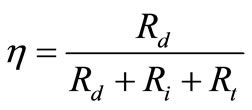 . (3)
. (3)
At Ri calculations it is supposed, that HF current in the inductor proceeds in a layer with the depth δи, and the inductor length depends on coil diameter Di and number of coils N [6]
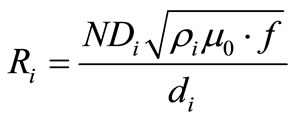 , (4)
, (4)
where di—diameter of inductor tube.
Electric resistance to HF currents can be defined from the assumption, that the width of a heating zone at small gap sizes h is equal to a projection of inductor diameter, and the length—to a ring π·NDd
 . (5)
. (5)
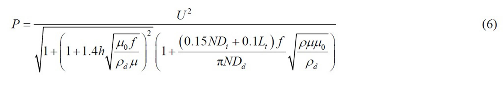
Electric resistance in the HF heating zone linearly decreases with the reduction of inductor coils number and detail diameter. The maximum values of efficiency for magnetic materials up to 0.9 - 0.95 are reached at Dd ≤ 0.01 m. After substitute expressions (2), (4), (5) in (1) and make the transformations we will receive expression for effective HF heating power [7] (Equation (6)).
Depending on the type of HF generator, effective voltage on inductor is 50 - 500 V. According to that, the heating power changes from 1 to 20 kW depending on magnetic and electric properties of materials (Figure 1).
In equal conditions magnetic materials require smaller specific power. The general law is nonlinear decrease in heating power depending on HF currents frequency that is connected with display of superficial effect. However decrease in frequency increases electrodynamics effect of the fused solder hashing and raises its’ spreading.
Thus the electronic devices soldering sensitive to an electric field, the choice of frequency is necessary out from a condition δ < , where H—thickness of a package wall. In this case intensity of field inside the package will be decreased in 100 times that excludes degradation of electronic components [8].
3. Experimental Techniques
For induction heating systems effects of affinity, ring and concentration of a magnetic field are common. But it is possible to create power lines concentration of a field on the set heating surface of a conducting body using magnetic conductor of the certain design. Two types of inductors were investigated: circular with internal (Figure 2(a)) and open-ended magnetic conductor (Figure 2(b)). The first scheme contained HF generator 1, circular inductor 2 with the cylindrical magnetic core 3, and pyrometer 4. The soldering details 5 placed on thermal insulator 6. In the second scheme the generator 1 was connected to a winding inductor with conductor 2 of ferromagnetic material. In a gap of magnetic conductor details 4 were heated. The winding of inductor is connected by a direct current to an input of regulating rectifier 3.
Frequency was controlled on an output of generator with accuracy 0.1 kHz; amplitudes of a voltage and a current—by universal digital voltmeter; time—by the timer with accuracy 0.1 s; temperature—by the device 6 with accuracy 1˚C. Intensity of HF field in a gap was perceived by a measuring framework and estimated by the device 7. Appearance of HF equipment for soldering is resulted on Figure 3.
4. Experimental Results and Discussion
Thermal dependences for the soldering of integrated circuits cases have shown influence of inductor’s circular design. Two inductor coils (2) in one plane owing to linear site of heating creates more uniform heating of package of the integrated circuit, assembly by soldering (Figure 4). It promotes greater full efficiency in 1.6 - 1.8

Figure 1. Heating power vs voltage and materials: 1. Copper; 2. Aluminum; 3. Iron; 4. Kovar.
 (a)
(a) (b)
(b)
Figure 2. Schemes of EM heating for soldering.

Figure 3. HF soldering equipment.

Figure 4. Thermal relationships in soldering zone.
times in comparison with two coils (1) and in 4 times with one coil (3). For the second heating scheme the analysis has shown that at the first stage (up to 10 s) speed of heating was 60˚C/s, and further has decreased up to 20˚C/s, in connection with increase in losses of energy due to radiation. When factor of overlapping of gap К > 1, dispersion of heat occurs with greater speed.
Materials with low electrical conductivity at overlapping gap optimum are heated up with a speed up to 50˚C/s. Heating speed of details in a magnetic gap falls with growth of frequency, because the intensity of an electromagnetic field decreases.
For improvement quality of soldering connections due to increase of the solder spreading area and fuller filling of capillary gaps with it in connection from the moment of the beginning solders spreading before the termination of the soldering details informed low-frequency vibrations by submission of an alternating current by frequency of 50 - 400 Hz and amplitude 1 - 10 A in inducing winding. The amplitude of vibrations of details made 0.5 - 1.0 mm.
The optimal parameters of HF heating with inductor with open-ended magnetic conductor: f = 300 kHz, H = 2.5 × 10⁴ A/m, current amplitude 1 - 10 A in inducing winding.
HF heating in frequency band 1000 - 2000 kHz has the greater dependence on size of capacity and electrophysical characteristics of materials. At capacity of heating of 1 kW intensity of a field makes 4.5 × 10⁴ А/m, and time of the soldering of magnetic materials—5 sec (Figure 5).
5. Conclusions
Modeling and investigation of HF electromagnetic heating has allowed to optimize heating speed in local zones of formation of soldering connections and to improve their quality due to joint action of superficial effects and electromagnetic forces. To small-sized details from nonmagnetic materials it is preferable to use inductor with a
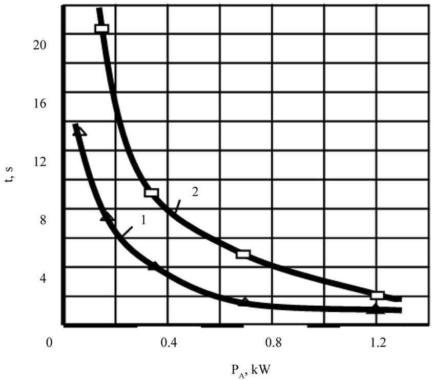
Figure 5. Soldering time—HF heating power relationship.
magnetic backlash as its’ working frequency much below, so it increases inductor’s efficiency.
Magnetic materials require smaller specific power of HF heating. The general law for all magnetic materials is nonlinear decrease in heating power depending on frequency of HF currents that is connected to display of superficial effect.
The optimal parameters of HF heating by inductor with open-ended magnetic conductor: frequency 300 - 400 kHz, intensity of magnetic field H = (2.5 4.5) × 104 A/m, current amplitude 1 - 10 A in inducing winding.
REFERENCES
- S. Lupi, Ed., “Induction Heating. Industrial Applications,” U.I.E., Paris, 1992, p. 142.
- S. Zinn and S. L. Semiatin, “Elements of Induction Heating: Design, Control, and Application,” ASM International, 1988, p. 335.
- M. Li, H. Xu, S.-W. R. Lee, J. Kim and D. Kim, “Eddy Current Induced Heating for the Soldering Reflow of Area Array Packages,” IEEE Transactions on Advanced Packaging, Vol. 2, No. 31, 2008, pp. 399-403. doi:10.1109/TADVP.2008.923385
- E. Rapoport and Y. Pleshivseva, “Optimal Control of Induction Heating Processes,” CRS Press, New York, 2007.
- V. L. Lanin, “Efficiency of Heating by Concentrated Flow of Energy in the Process of Soldering in Electronics,” Electronnaya Obrabotka Materialov, No. 2, 2002. pp. 17- 20.
- V. L. Lanin, “High Frequency Electro-Magnetic Heating in Electronic Systems Soldering Processing,” Electronnaya Obrabotka Materialov, No. 5, 2004. pp. 79-84.
- V. L. Lanin, “Modeling of HF Electro-Magnetic Heating during the Soldering of Electronic Devices,” News of the Belarus Engineering Academy, Vol. 2, No. 14, 2002, pp. 167-168.
- V. L. Lanin, A. P. Dostanko and E. V. Telesh, “Formation of Current-Carrying Connections in Electronics Products,” Publication Center of the BSU, Minsk, 2007, p. 574.