World Journal of Condensed Matter Physics
Vol.1 No.4(2011), Article ID:8773,4 pages DOI:10.4236/wjcmp.2011.14023
Multilayer Graphene Synthesized by CVD Using Liquid Hexane as the Carbon Precursor
![]()
Departamento de Materia Condensada y Criogenia, Instituto de Investigaciones en Materiales, Universidad Nacional Autónoma de
México, México.
Email: claudiabautistaf@gmail.com, doroteo@servidor.unam.mx
Received July 20th, 2011; revised August 15th, 2011; accepted August 30th, 2011.
Keywords: Graphene, chemical vapor deposition, hexane, transmittance
ABSTRACT
We produce multilayer graphene by the Chemical Vapor Deposition (CVD) method at atmospheric pressure and 1000˚C, using flexible copper substrates as catalyst and liquid hexane as the source of carbon. We designed an optical device to measure the transmittance of the carbon films; with this information we calculate that the approximate number of layers is 11.
1. Introduction
Since 2004, graphene has been proved to be a very interesting new material [1] because of its amazing optical, electrical and phononics, particular properties [2]. First of all, graphene is only one carbon thin layer with 0.34 nm thickness in a hexagonal arrangement, the so called honeycomb lattice. Electrons in graphene can travel trough the honeycomb lattice with a zero effective mass and without scattering, described by a 2D analog of the Dirac equation [3,4] with a Fermi velocity vF = 1 × 10⁶ m/s [5]. A half integer quantum Hall effect for both electron an hole carriers is observed in graphene [3,6], and the Klein paradox was also experimentally observed [7]. One of the most important features of graphene, which is relevant to our research, is that graphene’s absorbance is a universal constant given by: πα = π/137 = 2.3%, where α is the fine structure constant [8-10]. We use this quantity to estimate the number of layers of graphene in our graphitic films. Due to its unique properties, graphene synthesis has acquired a great interest. Chemical Vapor Deposition (CVD) is a useful method to produce large area graphene films on metal surfaces [11]. With the CVD method, metals such as Ni [12], Co [13], Ru [14], Ir [15] and Cu [11,12,16,17] are used; and CH4 or C2H2 as a source of carbon are employed [18,19]. Cu is the most used metal to produce large area graphene films [18-22]. Because of the versatility and cost, we prepared multilayer graphene on top of a Cu foil using hexane (C6H14) as a liquid precursor of carbon.
2. Experimental Details
We used Cu foils of 1.5 × 1.5 cm2 and 100 μm of thickness to grow multilayer graphene, using liquid hexane as a source of carbon. Our CVD system, with a container for liquids, is very versatile; we can change without difficulty the liquid hexane by other liquid precursor. Therefore, growth of graphene using liquid precursor have some advantages over gas precursor; one of these is, gas precursor are more expensive than a liquid one, but one of the most important issue is that using liquid phase it would be possible to dope graphene [23]. The Cu foils were immersed in a ferric nitrate (Fe(NO3)3∙9H2O) solution for a chemical polish during 2.5 hours to have a more uniform Cu surface; because carbon film take the morphology of the substrate in the CVD method, and we are interested in well structured few layer graphene.
Using a horizontal furnace, Cu foils were introduced at the center of a 70 cm long fused quartz tube with 2.5 cm internal diameter. We found that the better conditions to have the thinner films are the following: In a hydrogen atmosphere (473 sccm) the system go from room temperature to 1000˚C, at this time, we let to flow 4 sccm of H2 into a bubbler containing liquid hexane during 15 minutes into the quartz tube, after this time the hexane flow is cut off and the furnace is turned off. The hydrogen flow is maintained until the system was cooled to room temperature. The CVD system is presented in Figure 1.
After CVD process, Cu foils were etched using a ferric nitrate solution during the night, 100 mg of ferric nitrate in 20 ml of water. After this process, the carbon film is transferred to a deionized water bath to clean it, and finally captured with the desired substrate. Corning glass or fused quartz substrates for transmittance measurements were used, and copper grids for electron diffracttion characterization.
We know that graphene’s absorbance is of 2.3% and it is practically independent of wavelength in the visibleinfrared region. Furthermore, the absorbance of multilayer graphene increases with the number of layers, each graphene layer increases absorbance by 2.3% [10]. We use this approach to determine the number of layers of our multilayer graphene produced by the CVD method using liquid hexane as a source of carbon. To measure the transmittance of our films, we propose the experimental arrangement shown in Figure 2 (a).
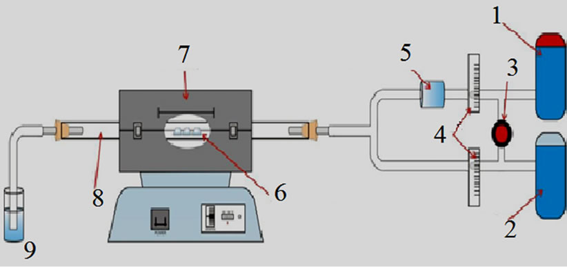
Figure 1. CVD system: 1: Hydrogen gas; 2: Argon gas; 3: Gas valve; 4: Flow controllers; 5: Hexane container (bubbler); 6: samples; 7: CVD furnace; 8: Quartz tube; 9: Water.
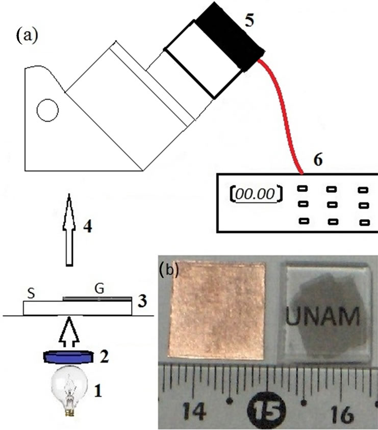
Figure 2. (a) Experimental arrangement for transmittance measurement: 1: light source; 2: filter; 3: sample where S means Substrate and G Graphene; 4: transmitted light collected by the objective of the microscope; 5: photodiode in place of the ocular; 6: electrometer. In (b), samples obtained by CVD on Cu and fused quartz (right) for optical characterization.
We adapted a photodiode (Infrared Industries, serial number 9002) in one of the ocular lenses of an optical microscope (Iroscope MO-64), to measure the transmittance of our multilayer graphene with white light, and color filters of 620 nm and 905 nm. The used objective was 60×, the transmitted light by the substrate and the film on the substrate were measured using the photodiode. In this case, the current generated in the photodiode and measured by the electrometer is proportional to the light intensity.
3. Results and Discussion
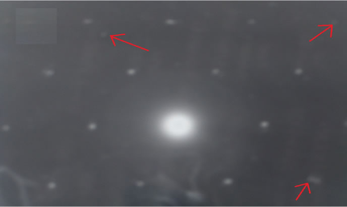
The electron diffraction pattern of our carbon films obtained by CVD method is shown in Figure 3 (a). We observed that when the sample is tilted respect to the electron beam, some diffraction spots change notably their intensities, such as those marked with arrows, indicating that we are dealing with multilayer graphene films [24].
The UV-Vis transmittance spectrum of our films is shown in Figure 3 (b) and it is similar to those reported for few layer graphene [19]. This spectrum shows an absorption peak around 268 nm, arising from resonant excitons [25], and in the visible-infrared range the transmittances is almost constant for a single layer graphene, but when the number of layers increases, the transmittance varies significantly in visible region, as in [19].
 (a)
(a)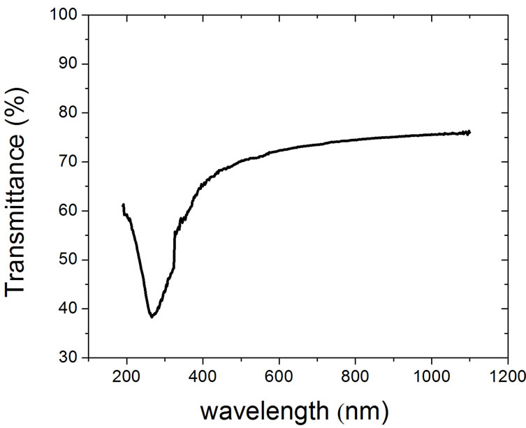 (b)
(b)
Figure 3. (a) Electron diffraction pattern of our multilayer graphene using JEOL, JEM-1200EX at 120 KV; (b) UV-Vis transmittance spectrum.
The measured transmittance of our samples obtained using the arrangement shown in Figure 2 is presented in Figure 4, we can see two important things, optical transmittance varies from white light to monochromatic light, and also between two specific wavelengths of incident light (620 nm and 905 nm). For the first one we can say that white light contains all wavelengths, and for the second one, the transmittance varies significantly when the number of layers increases, so we need to work only with monochromatic light near to the infrared region to have reliable results when we have multilayer graphene. If we generalize the use of a decrease in transmittance of 2.3% per layer, the results for 905 nm in Figure 4 give an average of 73.70% of the transmittance, which is equivalent to 11 layers approximately.
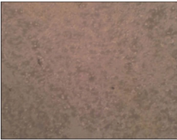
On the other hand, we performed a homogeneity analysis of the films measured by their optical transmittance (see Figure 5(a)) using the amount of red color in a digital image using the RGB system, such as the using in optical reflectance method [26].
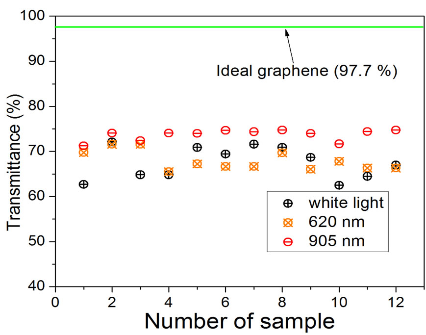
Figure 4. Transmittance obtained using white light and monochromatic light of 620 and 905 nm. Number of sample means different zones on the same macroscopic film, limited by the amplification generated by the 60× objective (300 μm of diameter approximately).
 (a)
(a)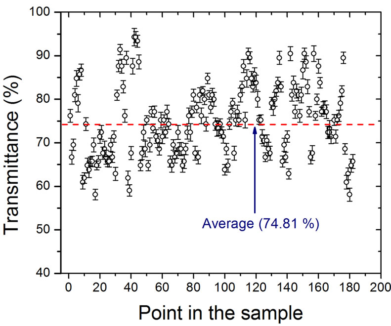 (b)
(b)
Figure 5. Homogeneity analysis, in (a) we show a digital image obtained by transmission of multilayer graphene films on top of a fused quartz substrate in (b) the value of the transmittance obtained from the digital image is shown.
The analysis was made point by point in the image of the substrate and the sample on top of the substrate using Corel Draw, the image was divided in a grid of 8 × 10 and in each point we took the amount of red color. Then, using the numbers generated by this software, the transmittance of the films can be calculated. With this analysis we have that our samples are homogeneous in 74.8% ± 8.3% in transmittance and, generalizing the criteria of 2.3% of absorbance per layer, we can say that our samples consist mainly of 11 layers but with some zones with 7 up to 14 layers of graphene, approximately.
4. Conclusions
We obtained multilayer graphene using CVD method with liquid hexane as a carbon precursor at atmospheric pressure. We implemented a method to measure optical transmittance of our multilayer graphene and, with this information the number of layers in each sample is estimated, around 11 in our samples. We also generalized the analysis of digital images to calculate the transmittance of the films, point by point.
5. Acknowledgements
The authors wish to thank Miguel Ángel Canseco Martínez and Carlos Flores Morales by support in UV-Vis and TEM measurements respectively.
REFERENCES
- K. S. Novoselov, A. K. Geim, S. V. Morozov, D. Jiang, Y. Zhang, S. V. Dubonos, I. V. Grigorieva and A. A. Firsov, “Electric Field Effect in Atomically Thin Carbon Films,” Science, Vol. 306, No. 5696, 2004, pp. 666-669. doi:10.1126/science.1102896
- A. H. Castro Neto, F. Guinea, N. M. R. Peres, K. S. Novoselov and A. K. Geim, “The Electronic Properties of Graphene,” Review of Modern Physics, Vol. 81, No. 1, 2009, pp. 109-162. doi:10.1103/RevModPhys.81.109
- K. S. Novoselov, A. K. Geim, S. V. Morozov, D. Jiang, M. I. Katsnelson, I. V. Grigorieva, S. V. Dubonos and A. A. Firsov, “Two-Dimensional Gas of Massless Dirac Fermions in Graphene,” Nature, Vol. 438, 2005, pp. 197-200. doi:10.1038/nature04233
- A. K. Geim and P. Kim, “Carbon Wonderland,” Scientific Ameican, Vol. 298, 2008, pp. 90-97. doi:10.1038/scientificamerican0408-90
- A. K. Geim, “Graphene: Status and Prospects,” Science, Vol. 324, No. 5934, 2009, pp. 1530-1534. doi:10.1126/science.1158877
- Y. Zhang, Y.-W. Tan, H. L. Stormer and P. Kim, “Experimental Observation of the Quantum Hall Effect and Berry’s Phase in Graphene,” Nature, Vol. 438, 2005, pp. 201-204. doi:10.1038/nature04235
- M. I. Katsnelson, K. S. Novoselov and A. K. Geim, “Chiral Tunnelling and the Klein Paradox in Graphene,” Nature, Vol. 2, 2006 pp. 620-625. doi:10.1038/nphys384
- L. A. Falkovski, “Optical Properties of Graphene,” Journal of Physics: Conference Series, Vol. 129, No. 1, 2008, pp. 012004-4. doi:10.1088/1742-6596/129/1/012004
- L. A. Falkovsky and A. A. Varllamov, “Space-Time Dispersion of Graphene Conductivity,” The European Physical Journal B, Vol. 56, No. 4, 2007, pp. 281-284. doi:10.1140/epjb/e2007-00142-3
- P. P. Nair, P. Blake, A. N. Grigorenko, K. S. Novoselov, T. J. Booth, T. Stauber, N. M. R. Peres and A. K. Geim, “Fine Structure Constant Defines Visual Transparency of Graphene,” Science, Vol. 320, No. 5881, 2008, pp. 1308. doi:10.1126/science.1156965
- X. Li, W. Cai, J. An, S. Kim, J. Nah, D. Yang, R. Piner, A. Velamakanni, I. Jung, E. Tutuc, S. K. Banerjee, L. Colombo and R. S. Ruoff, “Large-Area Synthesis of HighQuality and Uniform Graphene Films on Copper Foils,” Science, Vol. 324, No. 5932, 2009, pp. 1312-1314. doi:10.1126/science.1171245
- A. Reina, X. Jia, J. Ho, D. Nezich, H. Son, V. Bulovic, M. S. Dresselhaus and J. Kong, “Large Area, Few-Layer Graphene Films on Arbitrary Substrates by Chemical Vapor Deposition,” Nano Letters, Vol. 9, No. 1, 2009, pp. 30-35. doi:10.1021/nl801827v
- K. S. Kim, Y. Zhao, H. Jang, S. Y. Lee, J. M. Kim, K. S. Kim, J.-H. Ahn, P. Kim, J.-Y. Choi and B. H. Hong, “Large-Scale Pattern Growth of Graphene Films for Stretchable Transparent Electrodes,” Nature, Vol. 457, 2009, pp. 706-710. doi:10.1038/nature07719
- P. W. Sutter, J.-I. Flege and E. A. Sutter, “Epitaxial Graphene on Ruthenium,” Nature Mater, Vol. 7, 2008, pp. 406-411. doi:10.1038/nmat2166
- J. Coraux, A. T. N‘Diaye, C. Busse and T. Michely, “Structural Coherency of Graphene on Ir(111),” Nano Letters, Vol. 8, No. 2, 2008, pp. 565-570. doi:10.1021/nl0728874
- Y. Lee, S. Bae, H. Jang, S. Jang, S. E. Zhu, S. H. Sim, Y. I. Song, B. H. Hong and J. H. Ahn, “Wafer-Scale Synthesis and Transfer of Graphene Films,” Nano Letters, Vol. 10, No. 2, 2010, pp. 490-493. doi:10.1021/nl903272n
- X. S. Li, Y. W. Zhu, W. W. Cai, M. Borysiak, B. Han, D. Chen, R. D. Piner, L. Colombo and R. S. Ruoff, “Transfer of Large-Area Graphene Films for High-Performance Transparent Conductive Electrodes,” Nano Letters, Vol. 9, No. 12, 2009, pp. 4359-4363. doi:10.1021/nl902623y
- H. J. Park, J. Meyer, S. Roth and V. Ska´kalova, “Growth and Properties of Few-Layer Graphene Prepared by Chemical Vapor Deposition,” Carbon, Vol. 48, No. 4, 2010, pp. 1088-1094. doi:10.1016/j.carbon.2009.11.030
- S. Bae, H. Kim, Y. Lee, X. Xu, J.-S. Park, Y. Zheng, J. Balakrishnan, T. Lei, H. R. Kim, Y. I. Song, Y.-J. Kim, K. S. Kim, B. Özyilmaz, J.-H. Ahn, B. H. Hong and S. Iijima, “Roll-to-Roll Production of 30-Inch Graphene Films for Transparent Electrodes,” Nature Nanotechnology, Vol. 5, 2010, pp. 574-578. doi:10.1038/nnano.2010.132
- M. P. Levendorf, C. S. Ruiz-Vargas, S. Garg and J. Park, “Transfer-Free Batch Fabrication of Single Layer Graphene Transistors,” Nano Letters, Vol. 9, No. 12, 2009, pp. 4479-4483. doi:10.1021/nl902790r
- Y.-H. Lee and J.-H. Lee. “Scalable Growth of Free-Standing Gaphene Wafers with Copper (Cu) Catalyst on SiO2/Si Substrates: Thermal Conductivity of the Wafers,” Applied Physics Letters, Vol. 96, No. 8, 2010, p. 083101. doi:10.1063/1.3324698
- X. Li, C. W. Magnuson, A. Venugopal, J. An, J. W. Suk, B. Han, M. Borysiak, W. Cai, A. Velamakanni, Y. Zhu, L. Fu, E. M. Vogel, E. Voelkl, L. Colombo and R. S. Ruoff, “Graphene Films with Large Domain Size by a Two-Step Chemical Vapor Deposition Process,” Nano Letters, Vol. 10, No. 11, 2010, pp. 4328-4334. doi:10.1021/nl101629g
- A. Srivastava, C. Galande, L. Ci, L. Song, C. Rai, D. Jariwala, K. F. Kelly and P. M. Ajayan, “Novel Liquid Precursor-Based Facile Synthesis of Large-Area Continuous, Single, and Few-Layer Graphene Films,” Chemistry of Materials, Vol. 22, No. 11, 2010, pp. 3457-3461. doi:10.1021/cm101027c
- J. C. Meyer, A. K. Geim, M. I. Katsnelson, K. S. Novoselov, T. J. Booth and S. Roth, “The Structure of Suspended Graphene Sheets,” Nature, Vol. 446, 2007, pp. 60-63. doi:10.1038/nature05545
- L. Yang, J. Deslippe, C.-H. Park, M. L. Cohen and S. G. Louie, “Excitonic Effects on the Optical Response of Graphene and Bilayer Graphene,” Physical Review Letters, Vol. 103, No. 103, 2009, p. 186802(4). doi:10.1103/PhysRevLett.103.186802
- M. F. Craciun, S. Russo, M. Yamamoto, J. B. Oostinga, A. F. Morpurgo and S. Tarucha, “Trilayer Graphene Is a Semimetal with a Gate-Tuneable Band Overlap,” Nature Nanotechnology, Vol. 4, 2009, pp. 383-388. doi:10.1038/nnano.2009.89

