World Journal of Nano Science and Engineering
Vol.3 No.3(2013), Article ID:36677,8 pages DOI:10.4236/wjnse.2013.33011
Physical Properties of CrSb/InP(001): Effect of Interface in Half-Metallic
1Department of Physics, Kermanshah Branch, Islamic Azad University, Kermanshah, Iran
2Young Researchers and Elite Club, Kermanshah Branch, Islamic Azad University, Kermanshah, Iran
3Department of Physics, Kermanshah Science and Research Branch, Kermanshah, Iran
4Department of Physics, Faculty of Science, University of Guilan, Guilan, Iran
Email: *arash_bch@yahoo.com
Copyright © 2013 Arash Boochani et al. This is an open access article distributed under the Creative Commons Attribution License, which permits unrestricted use, distribution, and reproduction in any medium, provided the original work is properly cited.
Received June 18, 2013; revised July 23, 2013; accepted July 30, 2013
Keywords: Spintronic; Interface; Crsb-Inp; Density Functional Theory; GGA + U
ABSTRACT
In this study, density functional theory in improved flat waves’ framework has been used. First of all, characterization, elastic and half-metallic properties of the CrSb-ZB compound at (GGA & LDA) and GGA + U approximation are calculated. The elastic calculations indicate that the CrSb-ZB is a ductile material. However, the calculation of Deby temperature indicates that the CrSb-ZB is meta-stable. The half-metallicity character is also preserved at CrSb/InP (001) interface by GGA + U. The conduction band minimum (CBM) of CrSb in the minority spin case lies about 1.26 eV above that of GaSb, suggesting that the major spin can be injected into GaSb without being flipped to the conduction bands of the minor spin.
1. Introduction
Efficient spin injection from a ferromagnetic (FM) material into a semiconductor device has attracted considerable interest in recent years, but it’s still far from being fully understood [1]. One of the main challenges in spin injection is the impendence mismatch that arises between the spin source and the semiconductor substrate during the diffusive transport process [2]. The most significant advantage of using half metals (HM) instead of an ordinary metallic ferromagnet as a spin source is their ability to circumvent this obstacle and obtain efficient spin injection. Half-metallic ferromagnets have metallic behavior in one spin channel and semiconductor behavior in the other, leading to an integer number of total spin moment. So, in principle, a 100% spin polarization at the Fermi level is expected for these kinds of materials. A point worth noticing is that even if a material has halfmetallic character of the bulk regime, there is no guarantee to save such behavior on the surface, interface or even a dilute disorder around this area may significantly reduce the spin polarization at the Fermi level [3,4].
Recently many theoretical and experimental attempts have been done to investigate the HM properties of zinc blende (ZB) compounds such as MAs and MSb (M is a transition-metal elements) [5-10], which are compatible with III-V and II-VI semiconductors. Later, Liu [11] theoretically predicts that the ZB CrSb phase is a robust half-metallic ferromagnet with a magnetic moment of 3.00 µB per unit formula and its Half-metallic (HM) gap reaches 0.774 eV and persists to be nonzero even when it is compressed by 21%. A practical approach for stabilizing the CrSb compound in the metastable ZB structure is the pseudo morphic growth of CrSb thin film on ZB semiconductors. The lattice parameter of ZB CrSb has been calculated to be equal to 6.14 A˚ [11], which has a negligible difference with the experimental lattice parameters of InP (5.869 A˚) semiconductor [12]. Therefore ZB CrSb might be grown on ZB semiconductor such as InP. But it is important for practical applications whether or not the HM materials preserve the half-metallicity at surfaces and interfaces.
In this work, elastic and HM behaviors on ZB CrSb bulk and also HM properties CrSb/InP(001) interface have been theoretically investigated by using Density Functional Theory (DFT) approach. Optimization of bulk structure has been carried out by using GGA and adding GGA + U correction respectively in order to improve the electronic and magnetic results. U parameter is obtained by adjusting the bulk HM gap and magnetic moments and Cohesive energy (EC) with calculated value. The results are in a good agreement with experimental data.
2. Computational Methods
All calculations of this study are based on the spinpolarized DFT within the GGA and GGA + U approximation [13]. Due to some differences between the calculated data with GGA measurements of bulk magnetic properties of this alloy, we performed a more accurate electronic calculation by using GGA + U within Wien2K [14]. Basic function, charge density, and potential are expanded inside muffin-tin spheres in combination with spherical harmonic functions. The cut-off lmax equals 10 in Fourier series in the interstitial region. Moreover, parameter RKmax = 8. 50 is used which determines the matrix size (convergence), where R and Kmax are the smallest radii of all atomic spheres and the plane wave expansion cut-off outside the sphere respectively. The charge density was Fourier series expanded up to Gmax = 13 Ry1/2. The bulk and interface structures were simulated by using the cell and special approach with a regular K-Point mesh according to Monkhorest-Pack scheme [15].
3. Bulk Properties
The bulk calculations of ZB CrSb have already been reported in [9,11,16]. Here we focused on some new features of the bulk properties. First of all, we optimize the bulk elastic parameters within (GGA & LDA) and then the electronic structure and magnetic moments were calculated by using these optimized parameters. Crystals in cubic symmetry have only three distinct non vanishing elastic constants, namely C11, C12 and C44.
In order to calculate the values of parameters, the cubic unit cell is deformed by using appropriate strain tensors to yield energy-strain relation. The data depend on the symmetry which is used in the strain tensor. These data yield the specific elastic constant. In the present work, we have been using the strain tensors and the strain-energy relations described in [17].
The calculated elastic constants are listed in Table 1. The bulk modulus can be calculated from the elastic constants using the equation  which provides a useful internal consistency between various computational procedures. The mechanical stability of a crystal can be checked by means of the elastic constants which satisfies special restrictions for cubic materials. The stability criteria are described as B > 0; C11 − C12 > 0 and C44 > 0.
According to the Table 1 using GGA and LDA approximations and assuming that B > 0, C11 − C12 > 0 and C44 > 0, it is predictable that ZB structure is meta-stable.
The Shear modulus G, Young modulus E and Poisson, s ration υ for poly crystalline can be calculated from the elastic constants. The Shear modulus, a measure of the directional bonding is presented by Reuss and Voigt, s modulus, GR and GV [17,18]. The calculated values of G, E and υ for the ZB phase are presented in Table 1. The quotient of Bulk to Shear modulus (B/G) provides a simple empirical relationship between the plastic properties of materials and their elastic module. This quotient is introduced by Pugh, the B represents the resistance of fracture and G as the resistance to plastic deformation. According to GGA and LDA approximation and as can be concluded from Table 1, B and G are great and small respectively. A high value of this quotient points to the ductility of the materials, whereas a low value indicates its brittleness. The critical value is 1.75 which separates ductile and brittle materials [19], the high value of this quotient shows that the ZB structure is ductile. The (B/G) value for ZB CrSb is higher than 1.75 which indicates that this structure is ductile material. In the Debye model the mean sound velocity υm is connected to the longitudinal and transverse sound velocity, υl and υt respectively, which can be obtained from the elastic moduli as follow:
 (1)
(1)
 (2)
(2)
and
 (3)
(3)
Table 1. The elastic constants Cxx (GPa), Shear modulus G (GPa), Young modulus E (GPA), Poisson’s ratio v, mean sound velocity vm (m/s) and Debye temperature(K).
where ρ denotes the density of the material. Therefore the Debye temperature is given by [20],
 (4)
(4)
where N shows the number of atoms in the primitive unit cell and V0, h and kB are unit cell volume, Plank and Boltzmann constants respectively. The obtained Debye temperatures are listed in Table 1. By comparing LDA and GGA approximations, it is deduced that the calculated Debye temperature is small. The Debye temperature is a useful parameter in solid state problems. The Debye temperature obtained from elastic constants is close to the obtained one from low temperature specific heat measurement due to the main contribution of lattice vibrations. This evidence indicates that the ZB CrSb is in meta-stable phase according to the mechanical point of view.
Consistent with other reports, the calculated magnetic moment per formula unit (3.00 µB) which is obtained from GGA approximation [9,11,16] has a small spin flip gap. For better description of the electronic structure and magnetic moment of ZB CrSb, we applied the GGA + U scheme to our calculations to enhance the on-site electron correlation. The GGA lattice constant was adopted for GGA + U investigations and the electronic structure of the system was calculated at several values of effecttive U parameters. The obtained d Partial DOS (PDOS) at five selected values of U is presented in Figure 1. It is observed that the magnetic moment in all U is 3.00 µB. Therefor in the range of (U = 0. 25 − 0.30 Ryd) of the effective coulomb exchange integration, GGA + U predicts HM properties by the great spin flip gap.
Figure 1. The CrSb DOS by GGA + U approximation (U = 0. 1 Ry – 0.5 Ry).
By considering PDOS plots (Figure 1), as expected, it is observed that by increasing U value, the minority conduction states move toward higher energies. For all values of U between 0.1 Ry and 0.5 Ry give rise to the total magnetic moment of 3.00 µB. Applying the larger values in this interval leads large changes in electronic structure (Figure 1) which is in a good agreement with other works [9,11,16]. This large modification in GGA approximation needs strong arguments. By taking into account screening effects for transition-metal elements [21], we selected smaller values of this interval (U = 0. 30 Ryd). These values are efficient for producing measured magnetic moments and they are consistent with the first-principles of Hartree-Foch-calculation values of effective parameter U. Therefore, we used the GGA+U approximation for the electronic and magnetic calculation in the CrSb/InP (001) interface, by taking the parameter U equal as U = 0. 30 Ryd.
4. Interface
4.1. Electronic Properties
In this section, we study the structural and electronic properties of CrSb/InP (001) interface. We used super cells containing some atomic layers of the alloy in contact with some atomic layers of the semiconductor. In order to form an epitaxial interface, the in-plane lattice parameters of the CrSb were set to the lattice parameter of InP and perpendicular lattice constant was optimized by minimizing the total force per unit cell. The number of atomic layers in two materials is large enough, so we can assume that all atoms in the central layers have a bulk like behavior. There are different possibilities depending on which termination of two materials is being selected. We consider all four possible ideal interface terminations in (001) direction, including Cr-P, Cr-In, Sb-P and Sb-In terminations in the interface.
Table 2 is the results of the cohesive energy calculation for four interface termination. It is shown that Cr-P termination is more stable than the others. In order to investigate the interface effects on the electronic properties of the stable In-P-Cr-Sb (001) interface, the interface atomic DOS was calculated and it is plotted in Figure 2 by GGA + U approximation. It is obvious from Figure 2 that the HM property is preserved. We also conclude from Figure 2 that 100% spin polarization exists at the Fermi level. The atoms in the middle of sub-interface layers (Bulk like layer) will have the spin less semiconductor behavior. Up &down spins have the energy gap at the Fermi level. By comparing the In atom in sub-interface and In atom at the middle film (bulklike behavior), it is concluded that the states of electron at the bulk-like behavior are localized. Also, it is seen that the DOS of P atom at the middle layer of the film does not contain
Table 2. The Cohesive Energy (eV) for the possible interfaces.
magnetic property, but the P atom at the interface layer has the HM property. Also, the states of a P atom at the middle layer are localized but in the interface layer are broadened which shows the bounding property of P atoms at the interface.
Figure 2 shows that the Cr atom layers in the middle layer and the interface contain HM property, but the states of Cr atoms in the middle layer are localized and at the interface are broadened. By approaching the interface, the non-magnetic PDOS at InP substrate continuously change toward the ferromagnetic HM behavior in the CrSb film in such a way that the interface Cr atom exhibits a moderate exchange splitting. The p-d hybridization between P and Cr interface enhances the exchange interactions in the interface P while the s-p hybridization between interface P and In substrate weakens the exchange interaction. Another conclusion is that the DOS in both major and minor channels are shifted away from the Fermi level in comparison with the bulk Cr like state. This is due to the potential difference between the semiconductor and HM sides of the interface.
4.2. Band Alignment
One of the most important properties of the interface is band alignment. This quantity is relevant to transport control properties in hetrojunction devices. As a matter of fact, an HM/semiconductor junction behaves like a metal/semiconductor junction in the major-spin channel and a semiconductor/semiconductor in the minor-spin channel. In metal/semiconductor contacts, the relevant band alignment parameters are p-type or n-type Schottky barriers defined as the difference between semiconductor valance-band (VB) maximum (VBM) or conductionband (CB) minimum (CBM) and metal Fermi level; while in semiconductor/semiconductor contacts the valence-(conduction) band offset is defined as the difference between valance-(conduction) band edges in HM and semiconductor. In practice, to achieve the band diagram of a heterojunction, one may apply potential line-up to align two independently calculated bulk band structures of two materials. Within Local-Density Approximation (LDA) GGA calculations, the band gap of InP is not obtained consistent with experiment, so a scissors shift was applied to the conduction band of InP in order to fit the band gap with experimental values.
In order to determine the potential line-up parameter, we follow Peressi et al. and apply a two-step averaging scheme to the electrostatic potential at the interface [22].
Figure 2. Total DOS and PDOS of the CrSb/InP(001) interface by GGA + U approximation
First of all, the electrostatic potential was averaged over x-y planes in the supercell to obtain the in-plane average potential. The obtained average potential is shown in Figure 3 for the stable Cr-P termination as a prototype, and represents two periodic functions joining smoothly at the interface. The period of oscillations for these two functions are equal to half of the bulk lattice constants on both sides of the interface. The obvious offset of these two functions at the interface is the potential line-up. We determined the electrostatic potential line up of about 0.21 eV.
We used the obtained potential line-up and bulk electrostatic structure to determine the band diagram of the stable termination of CrSb/InP junction. Table 3 presents the obtained band alignment parameters along with band alignment parameters of some other similar hetero structure.
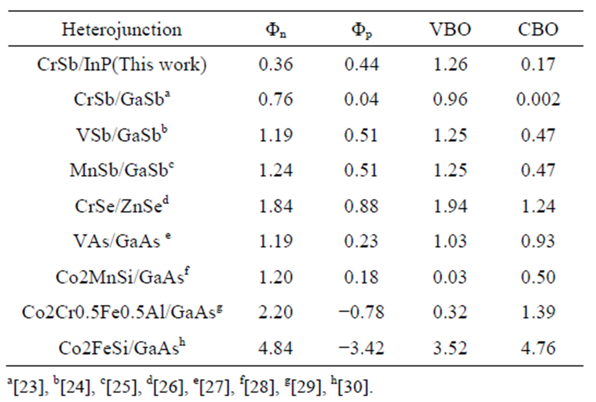
Table 3. The majority of Schottky barriers (eV) and minority of band offsets (eV) at CrSb/InP (001) heterojunction. Our results are compared with the band alignment parameters of some other half-metal/semiconductor heterojunction.
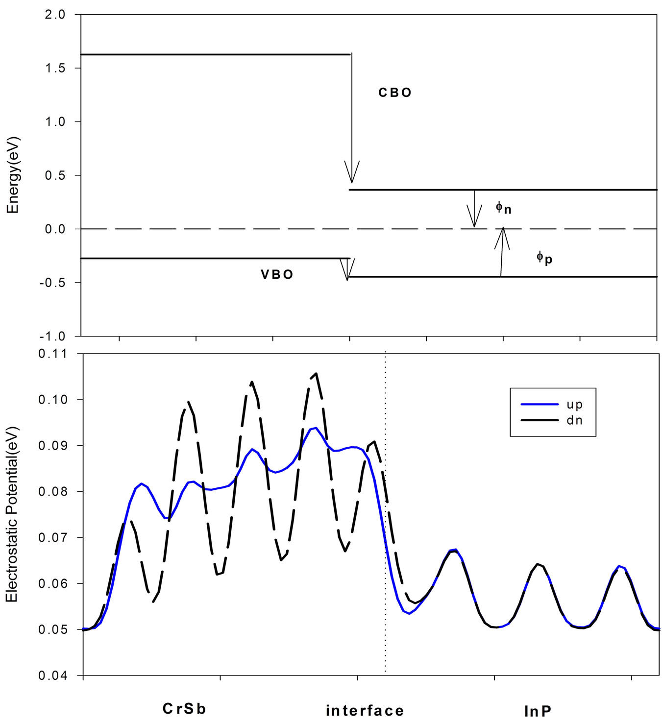
Figure 3. (a) The schematic band diagram at CrSb/IP (001) heterojunction. VB and CB stand for valence and conduction bands. The CrSb Fermi energy is set to zero. (b) The electrostatic potential at the CrSb/InP(001) interface in the up and dn spin.
Comparing with other Heusler alloy and binary halfmetal-based hetero structure, It is observed that CrSb/InP (001) hetero junction has a substantially larger valanceand conductionband offsets. These large offsets act as obstacles for spin junction from Heuslercntact into InP semiconductor in the spin-down channel. It is observed that the stable termination of this hetero structure has negative p Schottky barrier. The contribution of minor electrons of binary ZB half-metals in injected currents can lead to more efficient spin injection into semiconductors. It is shown that the Fermi level of CrSb lays below the CBM of InP semiconductor. This indicates that Schottky barrier can be formed for n-InP and a reverse bias should be applied in order to allow major spin to tunnel InP semiconductor.
Figure 3 also shows that as the CBM of minor spin in the CrSb lies at about 1.261 eV above the CBM of InP, the major spin of electrons can be directly injected to n-InP. In other word, the probability of electrons flipping to the CBs of minor spin under the applied reverse bias is decreased.
5. Conclusions
In this paper, the density-functional theory of the elastic (within GGA & LDA) and electronic properties (within GGA + U) of CrSb-ZB bulk have been reported. It is also deduced that CrSb-ZB structure is meta-stable. On the other hand, it is indicated that CrSb-ZB is a ductile material and the Debye temperature is small. When the effective coulomb exchange integration is located in the range of (U = 0.25 - 0.35), GGA + U predicts HM properties by the great spin flip gap.
It is also seen that at CrSb/InP (001) interface, the DOS and band alignment properties of atomic layers change coherently from the non-magnetic semiconductor substrate to ferromagnetic HM CrSb film. The DOS by the GGA + U at the interface shows that the HM property is retained. The interface band alignment parameters are determined and it is found that CrSb/InP(001) heterojunctions have a substantially higher minority valance band offset with respect to the Husler based heterojunction.
6. Acknowledgements
This work was jointly supported by the simulation of Nano Physics Lab center of Kermanshah Branch, Islamic Azad University. This work is the result of scientific research in the Kermanshah Branch, Islamic Azad University.
REFERENCES
- J. M. D. Coey and M. Venkatesan, “Lecture Note in Physics,” Springer, New York, 2002.
- G. Schmidt, D. Ferrand, L. W. Molenkamp, A. T. Filip and B. J. van Wees, “Fundamental Obstacle for Electrical Spin Injection from a Ferromagnetic Metal into a Diffusive Semiconductor,” Physical Review B, Vol. 62, No. 8, 2000, pp. R4790-R4793. doi:10.1103/PhysRevB.62.R4790
- S. Picozzi, A. Continenza and A. J. Freeman, “Role of Structural Defects on the Half-Metallic Character of Co2MnGe and Co2MnSi Heusler Alloys,” Physical Review B, Vol. 69, No. 9, 2004, Article ID: 094423. doi:10.1103/PhysRevB.69.094423
- L. J. Singh, Z. H. Barber, Y. Miyoshi, W. R. Branford and L. F. Cohen, “Structural and Transport Studies of Stoichiometric and Off-Stoichiometric Thin Films of the Full Heusler Alloy Co2MnSi,” Journal of Applied Physics, Vol. 95, No. 11, 2004, p. 7231. doi:10.1063/1.1667857
- T. Plake, M. Ramsteiner, V. M. Kaganer, B. Jenichen, M. Kastner, L. Daweritz and K. H. Ploog, “Periodic Elastic Domains of Coexisting Phases in Epitaxial MnAs Films on GaAs,” Applied Physics Letters, Vol. 80, No. 14, 2002, p. 2523. doi:10.1063/1.1467699
- K. Ono, J. Okabayashi, M. Mizuguchi, M. Oshima, A. Fujimori and H. Akinaga, “Fabrication, Magnetic Properties, and Electronic Structures of Nanoscale Zinc-Blende MnAs Dots (Invited),” Journal of Applied Physics, Vol. 91, No. 10, 2002, p. 8088.
- H. Akinaga, T. Manago and M. Sirai, “Material Design of Half-Metallic Zinc-Blende CrAs and the Synthesis by Molecular-Beam Epitaxy,” Japanese Journal of Applied Physics, Vol. 39, 2000, pp. L1118-L1120. doi:10.1143/JJAP.39.L1118
- M. Mizuguchi, H. Akinaga, T. Manago, K. Ono, M. Oshima, M. Shirai, M. Yuri, H. J. Lin, H. H. Hsieh and C. T. Chen, “Epitaxial Growth of Zinc-Blende CrAs/GaAs Multilayer,” Journal of Applied Physics, Vol. 91, No. 10, 2002, p. 7917. doi:10.1063/1.1455612
- J. H. Zhao, F. Matsukura, K. Takamura, E. Abe, D. Chiba and H. Ohno, “Room-Temperature Ferromagnetism in Zincblende CrSb Grown by Molecular-Beam Epitaxy,” Applied Physics Letters, Vol. 79, No. 17, 2001, p. 2776. doi:10.1063/1.1413732
- P. Radhakrishna and J. W. Cable, “Inelastic-Neutron-Scattering Studies of Spin-Wave Excitations in the Pnictides MnSb and CrSb,” Physical Review B, Vol. 54, No. 17, 1996, p. 11940. doi:10.1103/PhysRevB.54.11940
- B.-G. Liu, “Robust Half-Metallic Ferromagnetism in Zinc-Blende CrSb,” Physical Review B, Vol. 67, No. 17, 2003, Article ID: 172411. doi:10.1103/PhysRevB.67.172411
- L. Bornstein, “Numerical Data and Functional Relationships in Science and Technology,” Springer, Berlin, 1987.
- J. Perdew, K. Burke and M. Enzerhof, “Generalized Gradient Approximation Made Simple,” Physical Review Letters, Vol. 77, No. 18, 1996, pp. 3865-3868. doi:10.1103/PhysRevLett.77.3865
- P. Blaha, K. Schwarz, P. Sorantin and S. B. Trickey, “Full-Potential, Linearized Augmented Plane Wave Programs for Crystalline Systems,” Computer Physics Communications, Vol. 59, No. 2, 1990, pp. 399-415. doi:10.1016/0010-4655(90)90187-6
- H. J. Monkhorst and J. D. Pack, “Special Points for Brillouin-Zone Integrations,” Physical Review B, Vol. 13, No. 12, 1976, pp. 5188-5192. doi:10.1103/PhysRevB.13.5188
- M. Shirai, “Possible Half-Metallic Ferromagnetism in Zinc Blende CrSb and CrAs (Invited),” Journal of Applied Physics, Vol. 93, No. 10, 2003. p. 6844. doi:10.1063/1.1558604
- A. Mellouki, L. Kalarasse, B. Bennecer and F. Kalarasse, “First Principles Calculations of the Structural and Elastic Properties of the Filled Tetrahedral Compounds LiCdX (X = N, P, As),” Computational Materials Science, Vol. 42, No. 4, 2008, pp. 579-583.
- M. J. Mehl, B. M. Klein and D. A. Papaconstantopoulos, “Intermetalic Compounds: Principles and Practice,” In: J. H. Westbrook and R. L. Fleisher, Eds., Principles, John Wiley and sons, London, 1995, pp. 195-210.
- P. Ravindran, L. Fast, P. A. Korzavyi, B. Johansson, J. Will and O. Eriksoon, “Density Functional Theory for Calculation of Elastic Properties of Orthorhombic Crystals: Application to TiSi2,” Journal of Applied Physics, Vol. 84, No. 9, 1998, p. 4891. doi:10.1063/1.368733
- J. D. Walecka, “Fundamental of Statistical Mechanics: Manuscript and Notes of Felix Bloch,” Imperial Vollege Press and Word Scientific, Singapore, 2000. doi:10.1142/4522
- T. Bandyopadhyay and D. D. Sarma, “Calculation of Coulomb Interaction Strengths for 3d Transition Metals and Actinides,” Physical Review B, Vol. 39, No. 6, 1989, pp. 3517-3521. doi:10.1103/PhysRevB.39.3517
- M. Peressi, N. Binggeli and A. Baldereschi, “Band Engineering at Interfaces: Theory and Numerical Experiments,” Journal of Physics D: Applied Physics, Vol. 31, No. 11, 1998, p. 1273. doi:10.1088/0022-3727/31/11/002
- F. Ahmadian, M. R. Abolhassani, M. Ghoranneviss and M. Elahi, “Half-Metallicity Characteristic at Zincblende CrSb(0 0 1) Surfaces and Its Interfaces with GaSb(0 0 1) and InAs(0 0 1),” Physica B, Vol. 31, 2009, p. 5212.
- A. Boochani, M. R. Abolhasani, M. Ghoranneviss and M. Elahi, “First Principles Study of Half Metallic Properties of VSb Surface and VSb/GaSb (001) Interface,” Communications in Theoretical Physics, Vol. 54, No. 1, 2010, pp. 148-158. doi:10.1088/0253-6102/54/1/28
- E. Sartipi, A. Hojabri, A. Bouchani and M. H. Shakib, “First Principles Study of Half-metallic Properties at MnSb/ GaSb(001) Interface,” Chinese Journal of Chemical Physics, Vol. 24, No. 2, 2011, p. 155.
- E. Hazrati, S. J. Hashemifar, H. Akbarzadeh, “First Principles Study of Bulk CrSe and CrSe/ZnSe(001) Interface,” Journal of Applied Physics, Vol. 104, No. 11, 2008, Article ID: 113719. doi:10.1063/1.3039510
- R. Q. Wu, G. W. Peng and Y. P. Feng, “Properties of VAs/GaAs Interface from First Principles Study,” Journal of Physics: Conference Series, Vol. 29, No. 1, 2006, p. 150. doi:10.1088/1742-6596/29/1/028
- N. Ghaderi, S. Hashemifar, H. Akbarzadeh and M. Peressi, “First Principle Study of Co2MnSi/GaAs(001) Heterostructures,” Journal of Applied Physics, Vol. 102, No. 7, 2007, Article ID: 074306. doi:10.1063/1.2781529
- S. Zarei, S. J. Hashemifar, H. Akbarzadeh and Z. Haffari, “Half-metallicity at the Heusler alloy Co2Cr0.5Fe0.5Al(001) surface and its interface with GaAs(001),” Journal of Physics: Condensed Matter, Vol. 21, No. 5, 2009, Article ID: 055002. doi:10.1088/0953-8984/21/5/055002
- Sh. Khosravizadeh, S. Javad Hashemifar and H. Akbarzadeh, “First-Principles Study of the Co2FeSi(001) Surface and Co2FeSi/GaAs(001) Interface,” Physical Review B, Vol. 79, No. 23, 2009, Article ID: 235203. doi:10.1103/PhysRevB.79.235203
NOTES
*Corresponding author.