American Journal of Analytical Chemistry
Vol. 3 No. 8 (2012) , Article ID: 21910 , 4 pages DOI:10.4236/ajac.2012.38071
PMMA Polymer Membrane-Based Single Cylindrical Submicron Pores: Electrical Characterization and Investigation of Their Applicability in Resistive-Pulse Biomolecule Detection
1Department of Electrical and Computer Engineering, University of Saskatchewan, Saskatoon, Canada,
2TRLabs, Saskatoon, Canada,
3Department of Anatomy & Cell Biology, University of Saskatchewan, Saskatoon, Canada
Email: *m.hashemi@usask.ca
Received June 2, 2012; revised July 12, 2012; accepted July 26, 2012
Keywords: Nanopores; Electrophoretic Detector; Electrical Characterization; Ionic Current; Biomolecule Detector
ABSTRACT
Single cylindrical submicron pores in PMMA polymer membranes are micropatterned by electron beam lithography and integrated into all PMMA-based electrophoretic flow detector systems. Pore dimensions are 450 nm in diameter and 1 μm in length. The pores are electrically characterized in aqueous KCl electrolyte, exhibiting a stable time-independent ionic current through the pore with a noise level of less than 1% of the open-pore current. The current-voltage curves are linear and scale with electrolyte concentration. The negative surface charge of the membrane over-proportionally decreases pore conductance at low electrolyte concentrations (≤0.1 M) that are still beyond those typically applied in biological experiments. Pores do not exhibit rectification of current flowing through them, allowing for operation with either polarity. To allow for detection of yet much smaller particles, the described PMMA-based system also was successfully equipped with pores of 1.5 nm instead of 450 nm in diameter. This was achieved by introducing naturally occurring biological protein pores of α-hemolysin on a lipid bi-layer into the pre-patterned PMMA membrane of an assembled PMMA-based electrophoretic flow detector system. Characteristics of translocation events of single-stranded linear plasmid DNA molecules through the pores were recorded, and ionic current deductions during biomolecule translocation were clear and distinguished. Based on the presented submicron scale open pore ionic current transport properties, as well as the observed passage of DNA molecules through protein pores inserted into PMMA membranes, our current research proposes that all PMMA electrophoretic flow detectors exhibit an excellent potential for future use as biomedical resistive-pulse sensors, as long as pore dimensions match those of biomolecules to be detected.
1. Introduction
Resistive-pulse sensing (Coulter counting) is a powerful method for detection and characterization of microand nano-scale particles and biomolecules such as viruses, DNA molecules, and proteins [1-5]). The particles to be identified are added to an aqueous electrolyte in one of the two reservoirs separated by a thin membrane containing a single micro/nano pore. One electrode is placed in each reservoir, and an outer electric field induces an open-pore ionic current (Iopen) through the pore dragging the particles with itself. Transient changes in Iopen (temporary Iopen blockade events) will occur when a particle slightly smaller than the pore traverses (translocates). This resistive-pulse can be analyzed to derive information regarding the particle size and even its morphology, concentration in the electrolyte, and affinity for the pore [6,7]: pulse amplitudes in the ionic current through the pore are proportional to the volume of the passing particles, the frequency of pulses is related to the concentration of particles in a sample flowing through the pore, and the residence time of a particle in the pore is related to its structure, affinity towards the pore, as well as its velocity.
Biological ion channels are naturally occurring transmembrane proteins that connect intraand extra-cellular regions of a cell and control permeation of ions and small molecules from one side to the other. Ion channel proteins have been applied as resistive-pulse sensors or Coulter counters for ions and small molecules with dimensions comparable to the channels, typically a few nanometers [2,8,9]. The most commonly used protein nano pore is α-hemolysin [3,10]. However, the range of operating conditions and the lifetime of protein pores and biological membranes (lipid bi-layers) are limited [11]. Electrical leakage currents and physical instability are frequently observed in such membranes [12]. Furthermore, they cannot endure a wide range of pH-values, temperatures, applied trans-membrane potentials, or solvents, and they are sensitive to vibrations [10].
To overcome the disadvantages, considerable effort has been recently devoted toward the development of artificially micropatterned apertures in engineered inorganic membranes. These offer several advantages over their biological counterparts including size control over a wide range, increased chemical, electrical, mechanical, and thermal stability, tunable surface properties, and a potential for integration into different devices [13,14]. A variety of techniques has been used to fabricate single, synthetic micro/nano pores in solid-state membrane materials. The most widely used methods employ ion or electron beams to create pores in silicon nitride or silicon oxide membranes [13-15]. Such silicon-based membrane materials have been chosen for decades of fabrication experience (etching or sculpting processes) and general operations considerations (biocompatibility and mechanical, chemical and thermal stability). However, such pores usually poorly wet due to the comparatively hydrophobic nature of the structured membrane material, and the pore structure quality and reproducibility are also often limited.
Due to the aforementioned drawbacks, carbon-based membranes are recently getting increased attention (e.g. polyethylene terephthalate (PET), polyimide (PI), and graphene). Such polymer membranes offer increased hydrophilicity, and are also well adapted to microfluidic systems due to their low cost, flexibility, and ease of use in mass production [16,17]. These membrane materials, however, often create increased noise levels and are only a few percent successful in biomolecule detection experiments [18]. We now propose polymethyl meth acrylate (PMMA) as a novel membrane material for this kind of applications. PMMA can directly be patterned by lithographic techniques and has proven excellent structure quality and resolution when patterned by electron beam lithography (EBL) as well as X-ray lithography (XRL). It is a transparent thermoplast, allowing for an optical feedback during fabrication (alignment steps) and operations (filling of reservoirs, electrode positioning, etc.). This is a benefit almost exclusive to PMMA when compared to competing materials. PMMA is rated excellent for its biocompatibility, has therefore been used in many biomedical applications and microchip electrophoresis systems [19], and is a property advantageous for the current application as well. The comparatively high hydrophilicity of PMMA (contact angles with de-ionized water were reported to be between 71.7 ± 1.5 and 73.7 ± 1 for comparable PMMA grades by our group, [20] supports wetting properties in the micro fluidic domain. Finally, PMMA membranes offer typical advantages of thermoplasts, such as mechanical and thermal shaping, good electrical resistance, and long-term stability. This opens up the possibility to build the entire detector device (not only the membrane) of a single material, PMMA (also referred to as acrylics). This is a strategic advantage over hybridly integrated systems: potentially unbearable stress on the thin membrane induced by unmatched thermal expansion while heating during fabrication and/or operation is fundamentally eliminated. However, PMMA like most micropatterned polymers tends to build up a negative surface charge (likely to a larger extent than observed in silicon-based materials) which could be disadvantageous for the intended use. Eventually this surface charge might have to be addressed with additional processing steps (surface modifications, electrolyte modifications). Also, micropatterning sequences for PMMA, while being very precise, can be quite costly.
Based on the references given for this paper as well as verbal communications from various biochemists working with electrophoretic detectors, Table 1 tries to summarize major advantages and disadvantages of the different device concepts.
We believe the potential benefits of introducing PMMA as a membrane material for all-PMMA electrophoretic flow detectors aimed for future use as resistivepulse sensors for biomedical applications are very pro-
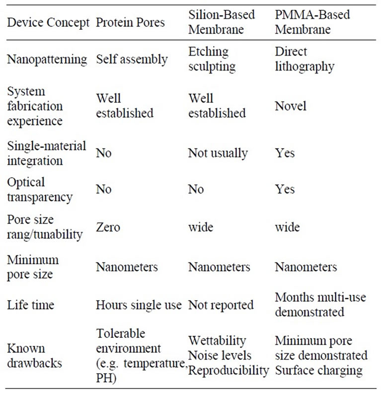
Table 1. Summary of major advantages and disadvantages of the different device concepts.
mising and outweigh the concerns mentioned above. We therefore chose to use EBL patterning as a rapid prototyping approach to prove the concept. Eventually, XRL could be applied for parallel, scaled-up fabrication of proven layouts. Recently we reported about the detailed layout of the membrane, including its mechanical properties, and initial fabrication steps [21].
Now, we give a concise overview over the EBL micropatterning and assembly sequence, complement EBL by self assembling a protein pore into the PMMA detector as a rapid prototyping approach to extend the area of applications by decreasing the pore size two orders of magnitude, electrically qualify and characterize the submicron pores, and report the first resistive-pulse sensing data on the transport of single stranded (SS) linear plasmid DNA molecules across a PMMA membrane of an all polymer electrophoretic flow detector system.
2. Membrane Micro/Nano-Patterning and Detector System Assembly
2.1. Electron-Beam-Based Sub-Micron-Sized Pores
Sacrificial silicon wafer substrates are cleaned with acetone and spin-coated (2500 rpm for 45 seconds) with a 1 µm-thick layer of MicroCHEM PMMA950A8 (molecular weight Mw = 950,000 g/mol), followed by baking in a convection oven at 170˚C for 30 minutes. This PMMA layer will later form the membrane freely suspended on a 1 mm diameter. The thickness of 1 µm is a compromise between patterning resolution (electron beam lithography (EBL) patterning with nanometer resolution requires as thin a layer as possible) and membrane mechanical stability for fabrication and operation [21]. In the subsequent lithography step, the layer is patterned by EBL (Raith 150 EBL system, University of Alberta NanoFab, Canada) with an exposure dose of 315 µC/cm2 and dip developed in methyl isobutyl ketone and alcohol (MIBKIPA 1:1) for 60 seconds. This sequence allowed to deliver a repeated test pattern with circular pores ranging from 200 nm to 1 mm in diameter. The silicon wafer is then diced and acrylic support rings of 300 µm thickness and 1 mm inner open diameter get aligned to each submicron pore, using 100 mm wide optical alignment markers which are also part of the EBL layout. The support rings get mounted and hermetically sealed to the PMMA layer using UV-initiated glue which we tested to be process compatible (lithography, assembly), long-term (3 months and more) operations compatible (electrolyte immersion), and biocompatible. The individual support rings each with a micropatterned PMMA layer attached are released by capillary forces from the silicon when soaked in de-ionized water containing a drop of surfacetant to decrease surface tension similar to the procedure recently published by Bae group in 2009 [22]. The water temperature is cycled between 80˚C (well below the glass transition temperature of PMMA; TG > 100˚C) for 10 minutes and room-temperature to facilitate capillary release by gentle thermal expansion. This delivers freely suspended, micropatterned PMMA membranes, each protected by a support ring. To prevent membranes from scratch similar support rings are glued to the other side of the membranes. Finally, a conductivity cell is created by UV-gluing two horizontally-oriented cylindrical reservoirs with an internal diameter of 6 mm and a length of 15 mm to each side of a supported micropatterned PMMA membrane unit. Each reservoir contains an upper inlet, through which an Ag/AgCl electrode as well as electrolyte solution (e.g. buffered potassium chloride, KCl) will get introduced for operations in a way that minimum differential geodetic pressure occurs across the membrane. Figure 1 (left) gives an aerial impression of such an assembled device with an overall length of approximately 30 mm. The right side of the figure depicts a schematic of the fundamental electrochemical process to take place in the device while operating.
Under the impact of an outer electric field induced by the electrodes, an ionic current through the pore drags molecules to be analyzed through the pore which partially block the volume of the channel, resulting in an increased impedance which can be detected by a pico ammeter in a patch clamp setup.
2.2. Self Assembled Nanometer-Sized Protein Pores
The pores fabricate by EBL to date have diameters of several hundred nanometers, with research aiming at further decreasing the size. As pore sizes determine the size range of translocating particles to be detected, a distinctively smaller pore size alternatively integrated into the same all-PMMA system setup would greatly increase the versatility of the system. In a rapid prototyping approach we therefore introduce α-hemolysin proteins which have a naturally occurring pore with 1.5 nm diameter into the PMMA detector membrane. Such pores have previously been applied in silicon-based systems, while we now extend the technique to allow for their implementation in a polymer microdevice. Such a process involves first attaching a lipid bi-layer across a micro pore in pre-patterned PMMA layer, followed by introducing the protein nano pore directly into the suspended lipid bi-layer.
Forces involved in applying the lipid bi-layer across the patterned PMMA layer mandate PMMA layer thicknesses comparable to the PMMA support ring (300 µm) rather than the PMMA membrane (1 µm). In this process sequence, the coated PMMA membrane is therefore omitted. Instead, the support ring is prepared with a reduced inner diameter of 200 µm (micro pore). Sharp
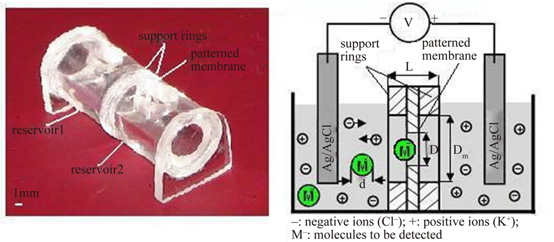
Figure 1. Aerial view of a microfabricated and assembled all-PMMA electrophoretic flow detector system consisting of a single submicron pore in a 1 μm thick PMMA membrane mounted between two support rings, sandwiched between two electrolyte reservoirs. The membrane separates the two-halves of a conductivity cell (left). Schematic of the fundamental electrochemical process to take place in the device while operating: An ionic current induced by electrodes also drags molecules to be analyzed through the pore, reducing the volume of the channel and resulting in an increased impedance (right).
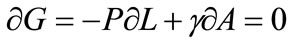
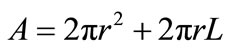
edges stemming from the micropatterning sequence might be detrimental to the lipid bi-layer. The micro pore surface therefore gets optimized using surface tension under the impact of broadband UV-exposure of the PMMA layer (exposure dose of 3600 µC/cm2). As a side effect this process also further reduces the micro pore diameter, and the process is terminated when the pore size gets close to a desired diameter of approximately 100 µm. The shrinkage was determined according to an analytical model originally presented by [14] for pores microfabricated in silicon dioxide (SiO2) membranes that are exposed to high energy electron beams. The model proposes that, when exposed to high-energy beams and thus high temperatures, all membrane materials have a physical characteristic to deform and lower their surface free energy by changing their surface area. Changes in surface area, in membranes containing a pore, will cause the pore to either shrink or expand in diameter, while its volume remains constant. As the proposed microfabrication sequence strongly depends on the smoothing and shrinking effect induced by the UV-exposure, we will briefly expand on the model as far as it pertains to the current layout:
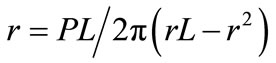
If γ is the surface energy density of a membrane with a constant uniaxial tension P, and the membrane contains a single cylindrical pore of radius r and constant thickness L at high temperatures, then the variation of total Gibbs free energy at equilibrium is given by
the change in free energy is obtained as:

In which
 and
and 
the surface energy density can then be written as:
The model describes that a membrane with a pore will lower its surface free energy when exposed to high- energy beams by reducing the pore radius if the pore had an original radius of r < L/2, whereas the pore size increases if the pore had an original radius size of r > L/2.
In agreement with the proposed model, the 300 µm thick PMMA layer with a micro pore of originally r = 100 µm < L/2 will lower its surface energy density when exposed to UV light by reducing its pore radius size during a shrinking process.
The smooth-surface, 100 µm wide micro pore in the 300 µm thick PMMA layer is subsequently integrated into an electrophoretic flow detector device as explained earlier for the support ring. Subsequently, a lipid bi-layer (or membrane) across the micro pore is formed by dipping a paintbrush into a lipid solution and painting across the micro pore as described by [23]. This comparatively forceful process is the reason why the PMMA layer has to be much thicker in this sequence when compared to the electron beam-based membrane microfabrication described above. The lipid solution is purchased from Avanti Polar Lipids Inc. (Alabaster, AL), vacuum-dried for 4 hours, and re-dissolved in decane to a final concentration of 30 mg/ml of lipid. Formation of a stable lipid bi-layer across the micro pore is identified by a complete blockade of Iopen through the micro pore in the PMMA layer when tested in a patch-clamp setup. In the final step, this lipid bi-layer will provide support for the protein nano pore.
α-hemolysin pores purchased from Sigma-Aldrich (St. Louis, MO) are prepared to a solution with the final concentration of 1.25 µg/ml. These α-hemolysin pores in solution are then self-assembled into the prepared lipid bilayer by injecting a total of 5 µl of protein nano pore solution adjacent to the micro pore in the PMMA layer. If performed during patch clamp testing, protein pore insertions are immediately detected by a characteristic jump in the Iopen value. According to [23], each inserted protein pore results in an Iopen value of approximately 100 pA when an external potential of +100 mV is applied across the membrane.
3. Electrical Characterization of a Single Cylindrical Electron-Beam-Based Sub-Micron-Sized Pore PMMA Detector System
A quantitative description of the steady-state ionic transport through the EBL-based micro pores is presented to prove the concept as a resistive-pulse sensor system for future biomedical applications. In particular, we present data on the long-term stability of the open pore current Iopen and its associated noise level, current-voltage characteristics of Iopen, impact of the electrolyte concentration on Iopen, as well as the conductance through a single cylindrical submicron pore as a function of electrolyte concentration. We also benchmark our system against previously published synthetic and biological counterparts.
3.1. Patch Clamp Measurement Setup
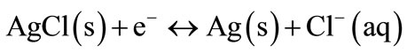
Both detector reservoirs are filled with buffered potassium chloride (KCl) electrolyte. The concentration of the aqueous electrolyte varies between 0.1 molar (M) and 0.75 M for the different experiments, representing typical molarities used in many biotechnological experiments. An Ag/AgCl electrode is introduced into the inlet of each half-cell, approximately 5 mm from the membrane.
A transmembrane negative potential is imprinted by the electrodes, inducing an open pore current Iopen through the pore. The amounts of Iopen and its eventual blockade are measured by pico ammeters and amplified (Axopatch 200B amplifier, Axon Instruments, Union City, CA), connected to a CV 203BU head-stage, and recorded by a PC running PClamp 10 (Axon Instruments) for later analysis. The entire measurement setup is located in a Faraday cage to eliminate potential external noise.
3.2. Pore Geometrical Characterization
Prior to any analysis of the pore performance, its geometry needs to be verified. Scanning Electron Microscopy (SEM) as the standard technique could not be applied in this case, because it immediately thermally alters the pore even at lowest acceleration voltages. This effect of electron beams on insulating organic material is widely known, and was also described for a similar case by [24]. However, Iopen measured by the patch clamp system itself is a quick, accurate and elegant way to electrically determine the pore diameter if the layer thickness and electrolyte conductivity are known. We recently described this technique [21,25] and derived our EBL-patterned pore dimensions to be consistently underestimated by approximately 150 nm. A pore with a nominal diameter of 300 nm, for instance, based its ionic conductance, is actually approximately 450 nm. The mismatch of about 150 nm in the specific processing sequence described above is attributed to EBL exposure and development process parameters not yet fully optimized, as well as potentially integration steps associated with membrane release. While such a diameter size deviation would certainly limit the use of our pore in actual sensing applications, and therefore needs to be optimised in future fabrication iterations, its subsequent electrical characterization can be performed by simply assuming the actual pore size of 450 nm.
3.3. Long-Term Stability of Iopen and Its Noise Level
The pores exhibit a very stable time-independent Iopen, with a very low level of noise over a wide range of applied voltages from 0 mV (control scenario) to 100 mV. This proves that the membrane neither deteriorates over time by excessive swelling, nor starts to leak. The level of noise is better than 1% of Iopen. Figure 2 demonstrates sample recordings of Iopen for 20 mV increments of the applied voltage (20 mV to 100 mV) over a time period of 10 minutes. The magnified inset spans 25 - 30 pA (noise level) around the average Iopen of 3.9 nA at 20 mV.
The current measured appears to be independent of the exact distance between each electrode and membrane as long as both electrodes are approximately placed in the same distance from the membrane, which is guaranteed by the system layout. Measurements are started 0.5 to 1 hour after filling the electrolyte to allow the pore to reach

Figure 2. Patch clamp measurement of the open pore current (Iopen, nA) through a single cylindrical submicron pore in a PMMA membrane as a function of time (min), in the presence of 0.1 M KCl and applied external voltages of 20 mV to 100 mV in 20 mV increments. Magnified inset demonstrates the noise level (approx. 1%).
its steady-state Iopen level. This setting time is usually attributed to the dynamics associated with wetting of the pore and removal of contamination layers: Contaminants from previous measurements, as well as contaminants in the electrolyte, would certainly add to the overall noise level. Both should therefore be minimized, and the setting time addresses at least the first point. In the present research, this setting time could be significantly reduced when drying of the pore after experiments is avoided by immersion into de-ionized water for storage immediately after each experiment, avoiding solidified contaminants in proximity of the pore.
The open pore current tests with various detector specimens also prove the hermetic seal of the system when measuring zero Iopen for detector specimens that had no pore patterned into the membrane: These control experiments without a pore do not reveal any ionic flow, i.e. exhibit infinitely large resistance, which demonstrates that the submicron pores in the actual devices form the only connection between the two half-cell detector compartments. The detector systems are tested for three months (some even up to a year) to show their long-term and multi-experiment stability. The measured time-independent steady-state ionic transport through the pore is reproducible within 10% - 15%, when a pore gets evacuated, washed with de-ionized water, and re-examined following the same procedure after a finite period of time.
To our knowledge, to date no other artificial synthetic micro/nano pore, patterned in either silicon-based substrates or polymer membranes, has exhibited such a good long-term stability with a low level of noise. The latter would, of course, likely increase with significantly decreasing pore size, because the relative tolerance and roughness would inevitably increase, polymer surfaceion interaction and charging get more important, and contaminants increase their relative importance.
The observed low noise level in the PMMA device when compared to other polymer materials can in part be attributed to micropatterning and material property models previously derived by various research groups: Ion transport properties of artificial micro/nano pores are strongly influenced by the chemical structure of the membrane as well as the microfabrication steps involved, including beam exposure and other accompanying pore development procedures [18]. For instance, the typical behaviour of the ion current versus time recorded at a constant voltage in the case of a polyethylene terephthalate (PET) membrane exhibited pronounced fluctuations with a high level of noise. Likewise do nano pores in polycarbonate (PC) foils present similar transport characteristics. In contrast, there was no fluctuation observed for pores microfabricated in polyimide (PI) by the same procedure of ion track etching [12,18]. The authors explain this difference with material properties related to imperfectly terminated polymer chains. Upon ion exposure-induced scission of polymer chains and subsequent chemical etching, carboxylate end groups are formed in, e.g., PET as well as in PI. In PET so called dangling ends are created due to the presence of ethylene components, which perform random movement, and thus fluctuations, when being immersed in a solution. The chemical structure of PI, on the other hand, is based on a planar sequence of aromatic groups, rendering a strong rigidity to the material, limiting the movement of PI polymer chains and thus fluctuations when immersed [18]. Smoothness and rigidity of the PI surface, thus, seem to be the decisive factors for a stable current. Both properties can be attributed to the submicron pore microfabricated in a PMMA membrane as well, partially explaining a low noise level.
3.4. Current-Voltage (I-V) Characteristics
As anticipated from above results, evaluation of open pore current-voltage (I-V) characteristics demonstrates a strong linear relationship. No saturation is observed for higher driving voltages, such that a wide range of voltages from 0 mV to +100 mV can be applied. Potassium chloride (KCl) electrolyte concentrations cover a typical range from 0.02 molar (M) to 0.75 M, with experiments conducted for five different concentrations (0.02, 0.05, 0.1, 0.5, and 0.75 M) (Figure 3). Further increasing the transmembrane potential to voltages beyond +100 mV does not damage the PMMA membrane and further increases the current through the submicron pore to higher values. This is in contrast to protein nano pores such as α-hemolysin, where a transmembrane potential of +100 mV produces a current value of approximately 100 pA [26], but a higher potential will result in damage to the
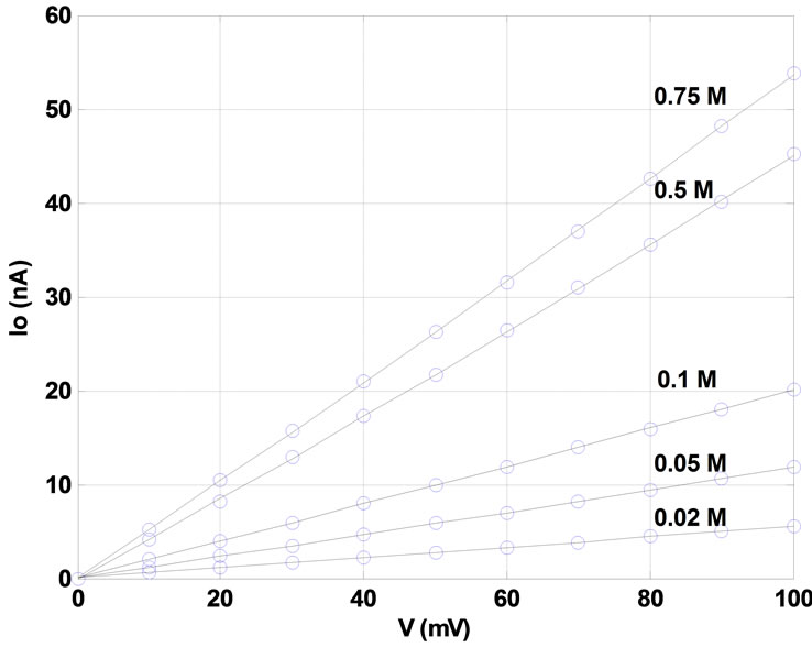
Figure 3. Patch clamp measurement of the open pore current (Iopen, nA) as a function of the applied voltage (mV) for 0.02, 0.05, 0.1, 0.5, and 0.75 M KCl concentrations.
lipid bi-layer membrane.
Figure 3 indicates that the I-V characteristics are not only linear, but that no current is observed at zero driving voltage. This relates to the transport mechanisms effective in our specific device (no diffusive contribution) and determines that reverse polarity device operation is possible: Three different transport mechanisms can contribute to the measured total steady-state ionic transport through a specific pore: convection (i.e., electro-osmotic flow driven by the electric field applied across a pore) [27], electrophoretic ion migration (driven by the electric field applied), and diffusion (driven by an electrolyte concentration gradient). Diffusion is the only contribution independent of the applied voltage. The devices exhibit zero current at zero voltage, indicating negligible diffusive transport contributions. Therefore, the electrolyte does not exhibit a concentration gradient across the pore for either of the tested molarities.
As a result, the same linear I-V relationship is maintained, when negative transmembrane potentials of 0 mV to –100 mV are applied (this voltage range is not depicted in Figure 3). More accurately, the amount of current measured through the pore at a certain negative transmembrane potential is approximately the same as that measured at a corresponding positive potential. Our pores, therefore, do not exhibit any rectification of the current flowing through them. Similar I-V relationships have been reported by other groups working with cylindrical nano pores [5,27,28]. This observation has two implications: First, the device can be operated in either direction (or polarity), which is also referred to as dual “on”-state, see below. Second, this indicates that our pores are actually cylindrically shaped, as a conical shape would typically exhibit rectification:
Asymmetric (non-cylindrical) pores such as basically all protein pores and conically shaped artificial pores exhibit current rectification. This can be explained by a model focusing on electrostatic interactions between ions passing through the pore and surface charge distribution on the pore walls [29]. Almost all microfabrication processes and their accompanying pore development steps leave artificial nano pores in either polymer membranes or silicon-based substrates with a net negative charge on their surface and walls [18]. The surface charge creates an asymmetric internal electrostatic potential inside the pore with a profile dependent on pore shape. Conical pores accumulate a much higher negative charge, and thus formation of a strong electrostatic trap, on the pore base compared to the pore tip. This electronic trap potential superposes with the applied trans-membrane potential induced by the electrodes, creating a preferred transport direction for positively charged ions towards the base [30-33]. As asymmetric nano pores reduce the ion flow in one direction, but promote it in the other, they are said to be either in the “on” state with much higher currents flowing through the pores, or in the “off” state with much less currents flowing through the pores. Artificial conical nano pores could therefore be called “voltagegated”, resembling some of their biological counterparts. The gated channels open and close in response to a specific chemical, mechanical, or electrical signal. This phenomenon, however, does not occur in symmetric cylindrical submicron pores with a homogenous surface charge distribution inside the pores, just like for the pores presented in this paper. It is often considered an advantage for such pores to be always in their “on” state of function regardless of the polarity of the applied transmembrane potential.
3.5. Impact of the Electrolyte Concentration on Iopen and the Cross-Pore Conductance
The electrical characterization of the detector system is expanded to the open pore current as a function of the electrolyte concentration. Figure 4 shows that the current monotonously increases with increasing concentration (0.02 M to 0.75 M) in an almost linear relationship. Applied voltages range from +10 mV to +100 mV.
Although standard electrolyte concentrations for biological experiments only range down to 0.1 M, we have still measured the current through our nano pore for the two additional electrolyte concentrations of 0.02 and 0.5 M. In accordance to the previous studies [29], we also identified that the dependence of the ionic current through a single artificial nano pore on the electrolyte concentrations deviates to a curve with a steeper slope at all the voltages applied as the electrolyte concentration is lowered to values below 0.1 M (Figure 4).
The observed phenomenon has been attributed to two effects: To an incomplete dissociation of the electrolyte at higher concentrations, and to the formation of an

Figure 4. Patch clamp measurement of the open pore current (nA) as a function of the KCl concentration for applied voltages ranging from 10 mV to 100 mV.
“electric double-layer”.
The negative surface charge on the PMMA membrane due to the formation of carboxylate end groups attracts K+ ions from the electrolyte to the pore surface and walls, forming an electric double-layer [4,29]. This double layer reduces the effective charges/potential available for the electrochemical transport mechanism. Its thickness depends on the salt concentration of the electrolyte close to the membrane: At lower salt concentrations, the relative concentration of K+ ions on the pore surface and walls is much greater compared to that in the bulk electrolyte area, determining a thicker double-layer, and therefore an elevated conductivity gradient or higher conductance.
Figure 5 illustrates this effect as it shows the measured conductance (reciprocal of the steady-state pore resistance, 1/Rp, nS) as a function of the electrolyte concentration. In agreement with the I-C data and theoretical model presented above, the pore conductance overproportionally increases with increasing electrolyte concentration at low concentrations. Our results are in close agreement with the data reported by other researchers fabricating cylindrical and conical nanopores in surface charged membranes [28,29].
As a remedy to this effect, the negative surface charge can be minimized or even neutralized by temporarily protonating the membrane surface which offers additional positive charge carriers, or by modifying the surface properties themselves for intermediate terms or permanently. Temporary protonation can be achieved by adjusting the electrolyte pH-value [18] to an acidic regime. We observed a pH-value of approximately 3 to neutralize the aforementioned effects. Whether such an approach would be compatible with the biological experiments might need further clarification.
Besides, the surface properties of the membrane can be modified for longer terms by either inducing chemical
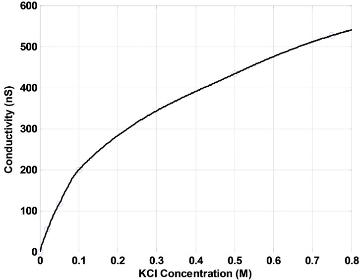
Figure 5. Patch clamp measurement of the conductance (nS) through single cylindrical submicron pores as a function of KCl concentrations of 0.02, 0.05, 0.1, 0.5, and 0.75 M.
reactions based on oxygen plasma treatment or by photochemical modifications involving UV surface exposure [33,34].
Besides these anormalities related to very low electrolyte concentrations, additional effects have been reported in literature at very high cocentrations for protein nanopores. These usually saturate, reaching a conductance plateau when the concentration is raised above a certain physiological level, which has been attributed to a limited binding-unbinding capacity. In comparison, artificial nanopores in solid-state membranes do not exhibit such saturated conductance patterns, allowing an application in a broader concentration range.
4. Biological Detector Testing: Transport of Single-Stranded Linear Plasmid DNA Molecules through α-Hemolysin Protein Pores Inserted into PMMA Membranes
The electrical characterization results of 450 nm wide EBL-based pores described in Section 3 are very promising for future detector applications and are considered a proof of principle for the all-PMMA detector approach. We are currently starting to test those pores with nanospheres of 100 nm diameter to verify the current blockade properties. First successful measurements have been performed, with resistive pulses in the 3.5% range.
Since the EBL-based pores do not yet allow to cover the full range of targeted particles in biomedical sensing applications, our present research also aimed at a rapid prototyping approach to extend the pore sizes available to a PMMA detector system down by two orders of magnitude, while in parallel optimizing the EBL nanopatterning capabilities. In this paper we report, for the first time, about inserting 1.5 nm wide nano pores naturally occurring in α-hemolysin proteins (compare Section 2.2) and their application in biomolecule detection. The fixed diameter of 1.5 nm happens to be slightly bigger than many DNA-based biomolecules, and therefore is a very interesting size for bio detectors. Figure 6(a) depicts a timeindependent steady-state stable open pore current Iopen of approximately 800 pA through α-hemolysin protein pores inserted into a PMMA membrane at an applied voltage of +100 mV. This current indicates the presence of eight protein pores in the PMMA membrane at the same time, as a successful insertion of a single α-hemolysin pore corresponds to an Iopen of around 100 pA. When no biomolecules are added to the electrolyte solution, Iopen remains constant and displays no significant deviations or deductions to lower or higher current values. Upon addition of single stranded linear plasmid DNA molecules to the negatively biased reservoir, numerous short temporal current blockade events occur. Individual resistive pulses for the eight pores combined are about 10% of Iopen, (Figure 6(b)), which can be extrapolated to
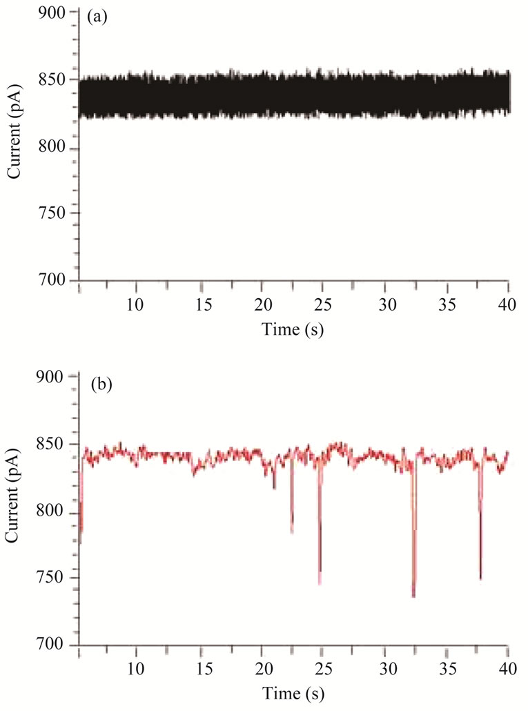
Figure 6. Patch clamp measurements of the open pore current (a) and current blockades/resistive pulses caused by translocation events of single stranded linear plasmid DNA molecules (b) through eight cylindrical protein pores in the PMMA detector at an applied external voltage of +100 mV.
a single pore resistive pulse of about 80%. After flushing out the molecules, the resistive pulses disappear. The observed events are therefore identified as translocation of DNA molecules through protein pores inserted into the PMMA membrane via a bi-layer.
5. Conclusions
In this paper, we have characterized the ionic flow through a novel PMMA membrane-based single cylindrical submicron pore patterned by electron beam lithography (EBL) integrated into an all PMMA electrophoretic flow detector. Experiments indicate that PMMA as the membrane material can help to overcome some of the drawbacks associated with lipid bi-layer or siliconor glass-based membranes, such as life time, wettability, opaqueness, and micro/nano patterning capabilities. The all-PMMA device approach further eliminates thermally induced stress. The pores described here are 450 nm in diameter, cutting across a 1 μm thick membrane. They exhibit open-pore ion transport properties that make them well suited for future resistive-pulse sensing applications.
Besides micropores patterned by EBL, we also report on the fabrication of nano pores two orders of magnitude smaller, in the same all-PMMA device. A combination of mechanical microfabriation, UV-exposure, and self-assembly of naturally occurring pores of 1.5 nm diameter in the protein α-hemolysin allowed for an investigation of translocation of single stranded linear plasmid DNA molecules. These experiments proved, for the first time, that a PMMA membrane is able to support the transport of biomolecules through microor nanofabricated pore, if pore dimensions are compatible to those of expected biomolecules to be detected.
REFERENCES
- H. Bayley and P. S. Cremer, “Stochastic Sensors Inspired by Biology,” Nature, Vol. 413, No. 6852, 2001, pp. 226- 230. doi:10.1038/35093038
- H. Bayley and C. R. Martin, “Resistive-Pulse Sensing: from Microbes to Molecules,” Chemical Reviews, Vol. 100, 2000, pp. 2575-2594.
- D. W. Deamer and D. Branton, “Characterization of Nucleic Acids by Nanopore Ananlysis,” Accounts of Chemical Research, Vol. 35, No. 10, 2002, pp. 817-825. doi:10.1021/ar000138m
- Z. Siwy, L. Troffin, P. Kohli, L. A. Baker, C. Trautmann and C. R. Martin, “Protein Biosensors Based on Biofunctionalized Conical Gold Nanotubes,” Journal of the American Chemical Society, Vol. 127, No. 14, 2005, pp. 5000-5001. doi:10.1021/ja043910f
- R. M. M. Smeets, U. F. Keyser, D. Krapf, M. Y. Wu, N. H. Dekker and C. Dekker, “Salt Dependence of Ion Transport and DNA Translocation through Solid-State Nanopores,” NanoLetter, Vol. 6, No. 1, 2006, pp. 89-95. doi:10.1021/nl052107w
- T. Ito, L. Sun and R. M. Crooks, “Simultaneous Determination of the Size and Surface Charge of Individual Nanoparticles Using a Carbon Nanotube-Based Coulter Counter,” Analytical Chemistry, Vol. 75, No. 10, 2003, pp. 2399-2406. doi:10.1021/ac034072v
- J. D. Uram and M. Mayer, “Estimation of Solid Phase Affinity Constants Using Resistive Pulses from Functionalized Nanoparticles,” Biosensors and Bioelectronics, Vol. 22, No. 7, 2007, pp. 1556-1560. doi:10.1016/j.bios.2006.06.020
- S. M. Bezrukov, I. Vodyanoy and V. A. Parsegian, “Counting Polymers Moving through a Single-Ion Channel,” Nature, Vol. 370, No. 6487, 1994, pp. 279-28. doi:10.1038/370279a0
- S. M. Bezrukov, “Ion Channels as Molecular Coulter Counters to Probe Metabolite Transport,” Journal of Membrane Biology, Vol. 174, No. 1, 2000, pp. 1-13. doi:10.1007/s002320001026
- J. Schmidt, “Stochastic Sensors,” Journal of Materials Chemistry, Vol. 15, No. 8, 2005, pp. 831-840. doi:10.1039/b414551h
- M. Mayer, J. K. Kriebel, M. T. Tosteson and G. M. Whitesides, “Microfabricated Teflon Membranes for Low-Noise Recordings of Ion Channels in Planar Lipid Bilayers,” Biophysical Journal, Vol. 85, No. 4, 2003, pp. 2684-2695. doi:10.1016/S0006-3495(03)74691-8
- A. Mara, Z. Siwy, C. Trautmann, J. Wan and F. Kamme, “An Asymmetric Polymer Nanopore for Single Molecule Detection,” NanoLetters, Vol. 4, No. 3, 2004, pp. 497- 501. doi:10.1021/nl035141o
- J. Li, D. Stein, C. McMullan, D. Branton, M. J. Aziz and J. A. Golovchenko, “Ion Beam Sculpting at Nanometer Length Scales,” Nature, Vol. 412, 2001, pp. 166-169. doi:10.1038/35084037
- A. J. Storm, J. H. Chen, X. S. Ling, H. W. Zandbergen and C. Dekker, “Fabrication of Solid-State Nanopores with Single-Nanometer Precision,” Nature Materials, Vol. 2, 2003, pp. 537-540. doi:10.1038/nmat941
- A. J. Storm, J. H. Chen, H. W. Zandbergen and C. Dekker, “Translocation of Double-Strand DNA through a Silicon Oxide Nanopore,” Physical Review, Vol. E71, No. 1, 2005, pp. 051903-051908.
- H. Shadpour, H. Musyimi, J. Chen and S. A. Soper, “Physicochemical Properties of Various Polymer Substrates and Their Effects on Microchip Electrophoresis Performance,” Journal of Chromatography A, Vol. 1111, No. 2, 2006, pp. 238-251. doi:10.1016/j.chroma.2005.08.083
- H. Bi, S. Meng, Y. Li, K. Gao, Y. Chen, J. Kong, P. Yang, W. Zhong and B. Liu, “Deposition of PEG onto PMMA Microchannel Surface to Minimize Nanospecific Adsorption,” Lab on a Chip, No. 6, 2006, pp. 769-775. doi:10.1039/b600326e
- Z. Siwy, P. Apel, D. Dobrev, R. Neumann, R. Spohr, C. Trautmann and K. Voss, “Ion Transport through Asymmetric Nanopores Prepared by Ion Track Etching,” Nuclear Instruments and Methods in Physics Research Section B, Vol. 208, 2003, pp. 143-148. doi:10.1016/S0168-583X(03)00884-X
- D. Belder and M. Ludwig, “Surface Modification in Microchip Electrophoresis,” Electrophoresis, Vol. 24, No. 21, 2003, pp. 3595-3606. doi:10.1002/elps.200305648
- T. Mappes, S. Achenbach and J. Mohr, “Hochauflösende Röntgenlithografie zur Herstellung polymerer Submikrometerstukturen mit groβem Aspektverhältnis,” Ph.D. Thesis, University of Karlsruhe, FZKA7215, 2006.
- M. Hashemi, S. Achenbach, D. Klymyshyn, B. Moazed and J. Lee, “Design and Microfabrication of a Polymer Membrane-Based Submicron Scale Electrophoretic Flow Detector for Biomedical Applications,” Microsystem Technology, Vol. 16, No. 8, 2009, pp. 1563-1567. doi:10.1007/s00542-009-1002-3
- J. S. Bae, S. C. Oh, J. E. Nam, J. K. Lee and H. J. Lee, “A tensile test technique for the freestanding PMMA thin films,” Current Applied Physics, Vol. 9, No. 1, 2009, pp. 107-109. doi:10.1016/j.cap.2008.08.029
- R. Stefureac, Y. T. Long, H. B. Kraatz, P. Howard and J. S. Lee, “Transport of α-Helical Peptides through α-Hemolysin and Aerolysin Pores,” Biochemistry, Vol. 45, No. 30, 2006, pp. 9172-9179. doi:10.1021/bi0604835
- S. Wu, S. R. Park and X. S. Ling, “Lithography-Free Formation of Nanopores in Plastic Membranes Using Laser Heating,” NanoLetters, Vol. 6, No. 11, 2006, pp. 2571-2576. doi:10.1021/nl0619498
- R. W. Deblois and C. P. Bean, “Counting and Sizing of Submicron Particles by the Resistive Pulse Technique,” Review of Scientific Instruments, Vol. 41, No. 7, 1970, pp. 909-915. doi:10.1063/1.1684724
- C. Dekker, “Solid-State Nano-Pores,” Nature, Vol. 2, 2007, pp. 209-215.
- C. Ho, R. Qiao, J. B. Heng, A. Chatterjee, R. J. Timp, N. R. Aluru and G. Timp, “Electrolytic Transport through a Synthetic Nanometer-Diameter Pore,” PNAS, Vol. 102, No. 30, 2005, pp. 10445-10450. doi:10.1073/pnas.0500796102
- L. Petrossian, S. J. Wilk, P. Joshi, S. Hihath, S. M. Goodnick and T. J. Thornton, “Fabrication of Cylindrical Nanopores and Nanopore Arrays in Silicon-on-Insulator Substrates,” Journal of Microelectromechanical Systems, Vol. 16, No. 6, 2007, pp. 1419- 1428. doi:10.1109/JMEMS.2007.908435
- B. Schiedt, K. Healy, A. P. Morrison, R. Neumann and Z. Siwy, “Transport of Ions and Biomolecules through Single Asymmetric Nanopores in Polymer Films,” Nuclear Instruments and Methods in Physics Research Section B, Vol. 236, 2005, pp. 109-116.
- Y. Choi, L. A. Baker, H. Hillebrenner and C. R. Martin, “Biosensing with Conically Shaped Nano-Pores and Nanotubes,” Physical Chemistry Chemical Physics, Vol. 8, No. 43, 2006, pp. 4976-4988. doi:10.1039/b607360c
- L. T. Sexton, L. P. Horne and C. R. Martin, “Developing Synthetic Conical Nanopores for Biosensing Applications,” Molecular BioSystems, Vol. 3, No. 10, 2007, pp. 667-685. doi:10.1039/b708725j
- Z. Siwy, Y. Gu, H. Spohr, D. Baur, A. Wolf-Reber, R. Spohr, P. Apel and Y. E. Korchev, “Rectification and Voltage Gating of Ion Currents in a Nanofabricated Pore,” Europhysics Letters, Vol. 60, No. 3, 2002, pp. 349-355. doi:10.1209/epl/i2002-00271-3
- J. M. Goddard and J. H. Hotchkiss, “Polymer Surface Modification for the Attachment of Bioactive Compounds,” Progress in Polymer Science, Vol. 32, No. 7, 2007, pp. 698-725. doi:10.1016/j.progpolymsci.2007.04.002
- J. Liu and M. L. Lee, “Permanent Surface Modification of Polymeric Capillary Electrophoresis Microchips for Protein and Peptide Analysis,” Electrophoresis, Vol. 27, No. 18, 2006, pp. 3533-3546. doi:10.1002/elps.200600082
NOTES
*Corresponding author.