Optics and Photonics Journal
Vol.2 No.3A(2012), Article ID:23304,4 pages DOI:10.4236/opj.2012.223035
Tunable Reflection Bands and Defect Modes in One-Dimensional Tilted Photonic Crystal Structure
1Department of Physics, Amity Institute of Applied Sciences, Amity University, Noida, India
2Department of Physics and Material Science and Engineering, Jaypee Institute of Information Technology, Deemed University, Noida, India
3Department of Physics, Shobhit University, Meerut, India
Email: sanjeev17th@yahoo.co.in
Received June 11, 2012; revised July 13, 2012; accepted July 25, 2012
Keywords: Photonic Crystal Structure; Photonic Band Gap (PBG); Omnidirectional Reflector; Tilted PC Structure; Defect Modes
ABSTRACT
We show theoretically that range of reflection bands and defect modes inside the band gap can be tuned by using a one-dimensional tilted photonic crystal (TPC) structure. A TPC structure is similar to the conventional PC structure with the only difference that in this case alternate layers are inclined at certain angle in the direction of periodicity of the structure. In order to obtain the reflectance spectra of the proposed structure transfer matrix method (TMM) has been employed. From the analysis of the reflectance curve, it is found that 100% reflectance range can be varied and enhanced by using TPC structure for both (TEand TM-) polarizations. The enhancement in reflection bands increases as the tilt angle increases for both the polarizations and hence the enlarged omni-reflectance bands are obtained. Further, we study the properties of the defect modes in TPC structure by introducing the tilted defect at the different tilt angle. The results show that defect modes (tunneling modes) can be tuned at different wavelengths by changing the tilt angle of the structure without changing other parameters. Finally, the effect of variation thickness of defect layers on the tunneling mode has been studied for both TPC and conventional PC structure. The proposed model might be used as a tunable broadband omnidirectional reflector as well as tunable tunneling or transmission mode, which has potential applications in the field of photonics and optoelectronics.
1. Introduction
During the past two and half decades photonic crystal (PC) structures have been an interesting and emerging field of research due to their ability to control and manipulate light inside the periodic structure. Photonic crystals also known as photonic band gap materials (PBG) are artificially fabricated periodic structures, which give rise to allowed and forbidden bands for the propagation of light. Photonic crystal structure leads to many potent applications in the filed of photonics and optoelectronics [1-8]. One of the potential applications of one-dimensional PC structure is omnidirectional optical reflector which is widely used in recent years, and a great deal of work has been done by the previous researchers [9-14]. One-dimensional PC is attractive since their production is more feasible at any wavelength scale and their analytical and numerical calculations are comparatively simple. The total reflection bands that occur in all directions for both the polarization (TEand TM-) are called omnidirectional reflectors or mirrors. Optical reflectors or mirrors are basically of two types, a metallic mirror and dielectric Bragg mirror. In metallic mirror, for arbitrary incident angles, light can be rejected over a wide range of wavelengths, however, at lower wavelengths, considerable amount of power is lost due the absorption. The mirrors based on multilayer dielectric structure have high reflectivity over a certain range of wavelengths but it is very sensitive to the incident angles. The omnidirectional reflectors based on PC have negligible loss compared with metallic mirrors, particularly at infrared, optical or higher frequencies. Broad band Omnidirectional reflection (ODR) region with high reflectivity of PC structure mainly depends on the two aspects; one on the selection of materials with high refractive index contrast and other on the proposed model. Several authors have proposed and developed the various model for attaining the broad band gap which includes encapsulation, identification of defects, nesting, multi-quantum well, photonic hetero structures etc. [9-16].
In the present communication we propose one-dimensional tilted photonic crystal (TPC) structure for further improvement in the model and enhancement in the omnireflectance region. A TPC structure is similar to the conventional PC structure with the only difference that in this case alternate layers are inclined at certain angle in the direction of periodicity of the structure. The proposed structure consists of a periodic array of two alternate layers of SiO2 and Si with low and high values of refractive indices as in the conventional PC structure. Reflectance spectrum of the proposed structure has been calculated by using the transfer matrix method (TMM). Further, we investigate the defect modes in TPC structure by introducing the tilted defect at the different tilt angle for two different thicknesses of the defect layer. It is observed that defect mode can be tuned by varying the tilt angle without changing other parameters of the structure. We consider here the Si-based material in the structure because silicon (Si) gives the actual optical integration and it is a good material for the fabrication of photonic devices. It has a large refractive index with excellent mechanical and thermal properties and is compatible with Si-based microelectronics. Thus, the characteristics of Si in combination with the SiO2 material have been investigated extensively and an omnidirectional reflector produced by them has also been reported.
2. Theoretical Analysis
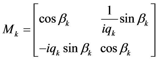
The periodic multilayered structure consists of alternate layers of high and low refractive index along the x-axis and placed between semi infinite media of refractive indices ni (refractive index of the incident medium) and nt (refractive index of the substrate) is illustrated in the Figure 1. The characteristics matrices for the TE (s-polarization) and TM (p-polarization) waves have the form [17,18]
 (1)
(1)
where ,
,  for the TE wave and
 for the TM wave,
 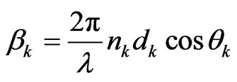 θk is the ray angle inside the layer of refractive index nk and λ is the wavelength in the incidence medium. For the tilted PC structure, due to the tilt angle of the plane of periodic multilayer structure with respect to x-axis (direction of periodicity), the thickness of low (d1) and high (d2) refractive index layers are modified and may be given as
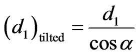 and
and . Here,
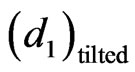 and
and 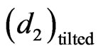 are the thickness of tilted layers of low and high value of refractive indices; α is the tilt angle.
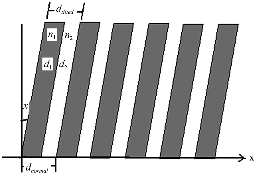
Figure 1. The schematic diagram of tilted photonic crystal structure.
The total characteristics matrix for the N period of system is given by
 (2)
(2)
The reflection coefficient of the multilayered structure for TE (s-polarized) and TM (p-polarized) waves are given by [18]
 (3)
(3)
 (4)
(4)
where M11, M12, M21, M22 are the elements of the total characteristic matrix of the N period multilayer structures. The values of q0 and qt for TE(s) and TM (p) polarized waves are given as
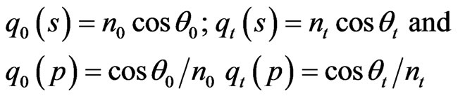 (5)
(5)
Reflectance spectra of multilayer structure can be obtained by using the expression:
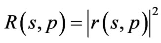 (6)
(6)
Neglecting the absorption loss of the materials, expression for the transmittance spectra can be written as
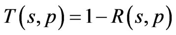 (7)
(7)
In the next section we present the numerical analysis of the proposed TPC structure for different tilt angle and show the omni-reflectance bands for both TEand TMpolarizations. Also, numerical computation of the presence of defect modes in the band gap regions has been presented.
3. Results and Discussions
For the numerical computation we choose SiO2 (n1 = 1.5) and Si (n2 = 3.5) layers and their thicknesses are taken in accordance with the quarter wave stack condition, i.e. 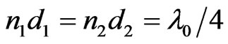 where λ0 = 1.55 μm, which comes out to d1 = 258.3 nm and d2 = 110.7 nm respectively. Here, we consider the case when both the layers are tilted with the horizontal direction and the total number of pair of layer taken as N = 15, the refractive index of the substrate is nt = 1.5and light is incident from air. The reflectance spectra of multilayer structure (AB)15 for different tilt angle α = 0˚, 10˚, 20˚ and 30˚ at incident angle θi = 0˚ and 85˚ are plotted in the Figures 2-9. At the normal incident angle it is found that range of 100% reflection bands increases when the tilt angle increases. For tilt angle α = 0˚ (structure is normal PC structure) width of reflection band is 863.4 nm for both TEand TM-mode. When tilt angle has value α = 10˚, 20˚ and 30˚ the width of reflection bands found to be 867.6 nm, 909.3 nm and 986.7 nm respectively. Due to increase in the tilt angle not only the width of reflection band increases but the
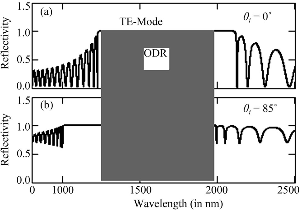
Figure 2. The reflectance spectra (TE-mode) of PC structure at tilt angle α = 0˚ for n1 = 1.5, n2 = 3.5, nt = 1.5 d1 = 258.3 nm, d2 = 110.7 nm, N = 15 layers (a) θi = 0˚; (b) θi = 85˚.
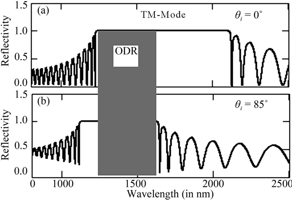
Figure 3. Represents the reflectance spectra (TM-mode) of PC structure at tilt angle α = 0˚ for n1 = 1.5, n2 = 3.5, nt = 1.5, d1 = 258.3 nm, d2 = 110.7 nm, N = 15 layers, (a) θi = 0˚; (b) θi = 85˚.
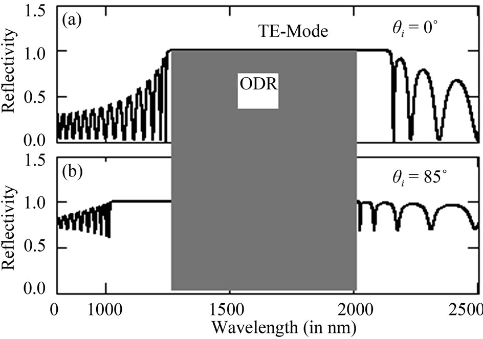
Figure 4. Represents the reflectance spectra (TE-mode) of PC structure at tilt angle α = 10˚ for n1 = 1.5, n2 = 3.5, nt = 1.5, d1 = 262.3 nm, d2 = 112.4 nm, N = 15 layers, (a) θi = 0˚; (b) θi = 85˚.
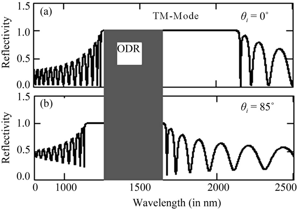
Figure 5. Represents the reflectance spectra (TM-mode) of PC structure at tilt angle α = 10˚ for n1 = 1.5, n2 = 3.5, nt = 1.5, d1 = 262.3 nm, d2 = 112.4 nm, N = 15 layers, (a) θi = 0˚; (b) θi = 85˚.
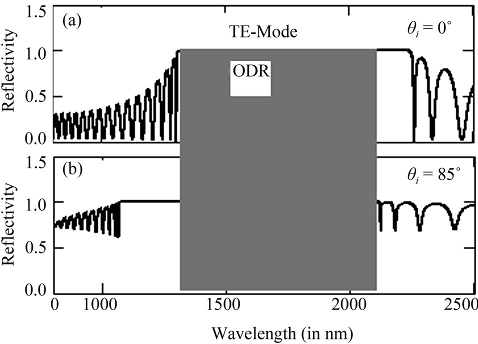
Figure 6. Represents the reflectance spectra (TE-mode) of PC structure at tilt angle α = 10˚ for n1 = 1.5, n2 = 3.5, nt = 1.5, d1 = 274.9 nm, d2 = 117.8 nm, N = 15 layers, (a) θi = 0˚; (b) θi = 85˚.
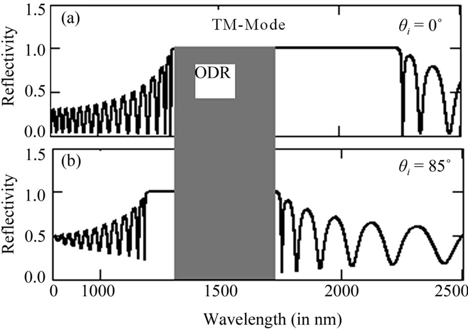
Figure 7. Represents the reflectance spectra (TM-mode) of PC structure at tilt angl α = 10˚ for n1 = 1.5, n2 = 3.5, nt = 1.5, d1 = 274.9 nm, d2 = 117.8 nm, N = 15 layers, (a) θi = 0˚; (b) θi = 85˚.
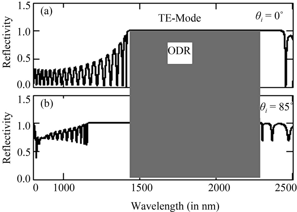
Figure 8. Represents the reflectance spectra (TE-mode) of PC structure at tilt angl α = 10˚ for n1 = 1.5, n2 = 3.5, nt = 1.5, d1 = 298.3 nm, d2 = 127.8 nm, N = 15 layers, (a) θi = 0˚; (b) θi = 85˚.
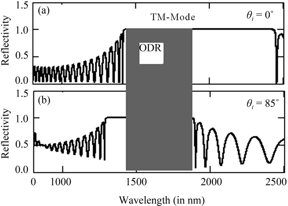
Figure 9. Represents the reflectance spectra (TM-mode) of PC structure at tilt angle α = 10˚ for n1 = 1.5, n2 = 3.5, nt = 1.5, d1 = 298.3 nm, d2 = 127.8 nm, N = 15 layers, (a) θi = 0˚; (b) θi = 85˚.
range of reflection bands shift to higher side of the wavelength, also. For the incident angle θi = 85˚ the TEand TM-modes have different range of reflection bands and so the band width. It has been observed that for tilt angle α = 10˚, 20˚ and 30˚ width of reflection bands in TEmodes are 978.4 nm, 992.5 nm 1040.3 nm and 1128.7 nm while for TM-modes it is found to be 487 nm, 494 nm 518.2 nm and 592.3 nm respectively. If we compare the range of reflectance bands for tilt angle α = 10˚ and 30˚ at normal incident angle, then we see that width of reflection band increases from 863.4 nm to 986.7 nm, i.e. there is increase of 14.2% in band width as compared to normal PC structure for both TEand TM-polarizations. When incident angle is 85˚ then for TE-mode width of reflection bands increases from 978.4 nm to 1128.7 nm and for TM-mode it increases from 487 nm to 592. 3 nm. This means that there is 15.2% enhancement in the width of reflectance band in TE-mode and 21.6% enhancement in TM-mode when the PC structure is tilted from 0˚ to 30˚. The omnidirectional reflection (ODR) bands corresponding to tilt angle α = 10˚ and 30˚ lies in the range 1223.6 nm - 1610.4 nm (= 386.8 nm) and1423.2 nm - 1859.5 nm (= 436.3 nm) respectively, which shows that total percentage enhancement in ODR range is 12.7%. From above discussion it can be inferred that by tilting the structure reflectance range and hence the ODR region can be enhanced appreciably without changing the other physical or optical parameters of the structure. The basic reason for the enhancement in the reflectance band of TPC structure is due to increase in the optical path length of layers, when the structure is tilted at certain angle from the horizontal direction, i.e. with direction of the periodicity of the structure. Now we show the numerical calculation of defect modes or tunnelling modes present in the reflection bands of normal and tilted PC structure. Figures 10-13 show the defect modes appearing in the band gaps of TPC structure having the form (AB)5 D(AB)5 for tilt angle α = 10˚, 20˚ and 30˚. For the calculation we choose air and ZnS as a defect medium with thickness taken as  and
and , where dD and nD denotes the thickness and refractive index of the defect layer respectively. Further, the thickness of defect layers at tilt angle (α) can be calculated by using the relation
 . Existence of defect modes or tunnelling modes in the band gap region of PC structure arises due to constructive interference of incident and reflected waves in the defect layer. From the analysis of Figures 10 and 11, it can be observed that when the thickness of defect layer is equal to
 , there exists only one defect mode in both cases where the defect layer is air or ZnS. If the tilt angle increases from 0˚ to 30˚ then the defect mode shifts to higher side of the wavelength. When the refractive index of defect layer is
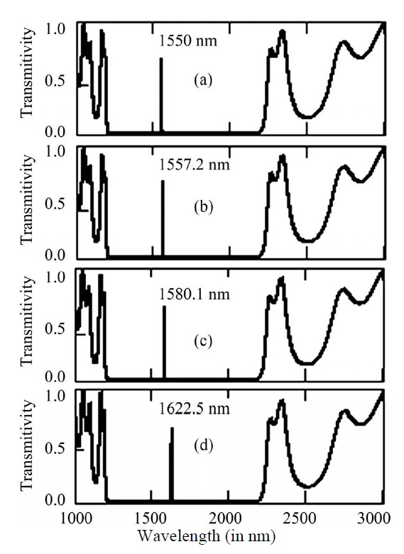
Figure 10. Represents the defect mode inside the band gap of structure (AB)5D(AB)5 for n1 = 1.5, n2 = 3.5, nD = 2.3 nm nt = 1.5 with dD = 168.5 nm for θi = 0˚ at tilt angle (a) α = 0˚; (b) α = 10˚; (c) α = 20˚ and (d) α = 30˚ respectively.
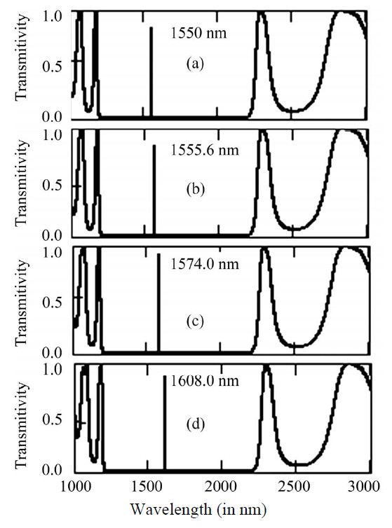
Figure 11. Represents the defect mode inside the band gap of structure (AB)5D(AB)5 for n1 = 1.5, n2 = 3.5, nD = 1.0 nm nt = 1.5 with dD = 387.5 nm for θi = 0˚ at tilt angle (a) α = 0˚; (b) α = 10˚; (c) α = 20˚ and (d) α = 30˚ respectively.
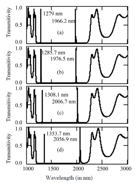
Figure 12. Represents the defect mode inside the band gap of structure (AB)5D(AB)5 for n1 = 1.5, n2 = 3.5, nD = 2.3 nm nt = 1.5 with dD = 337.0 nm for θi = 0˚ at tilt angle (a) α = 0˚; (b) α = 10˚; (c) α = 20˚ and (d) α = 30˚ respectively.
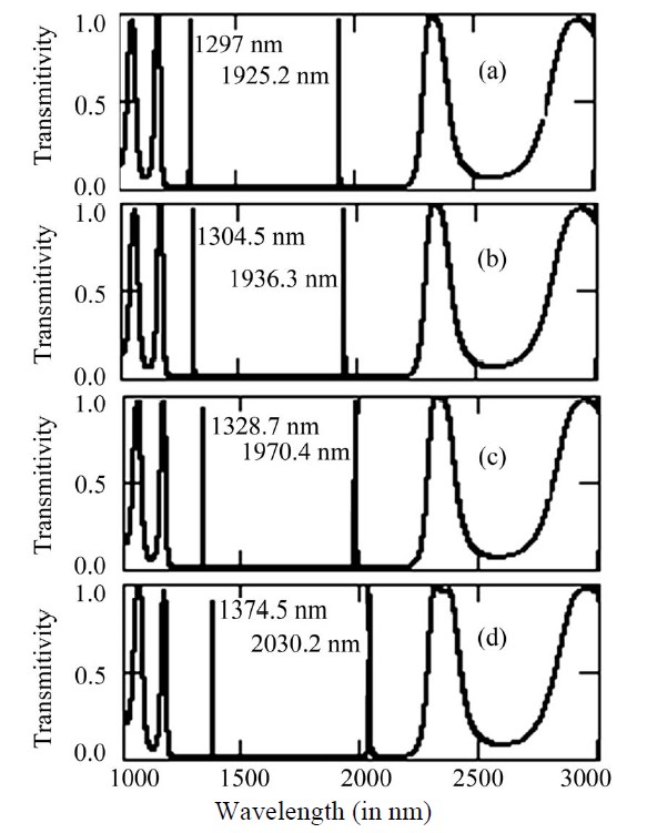
Figure 13. Represents the defect mode inside the band gap of structure (AB)5D(AB)5 for n1 = 1.5, n2 = 3.5, nD = 1.0 nm nt = 1.5 with dD = 775.0 nm for θi = 0˚ at tilt angle (a) α = 0˚; (b) α = 10˚; (c) α = 20˚ and (d) α = 30˚ respectively.
larger than one of the constituent layers (n1 and n2) forming the structure (here it is ZnS with refractive index nD = 2.3), then tunnelling mode has transmission peak nearly equal to 67%. But when the refractive index of defect layer is smaller than n1 and n2 (here we take air nD = 1.0) then the transmission peak has value nearly equal to 85% for α = 0˚ and 10˚ while it approaches to 95% for α = 20˚ and 30˚. Further it has been observed that when the thickness of defect layer is in accordance with quarter wave stack condition then the tunnelling mode lies towards the lower wavelength side of the reflection bands for each tilt angle. From Figures 12 and 13, we notice that by increasing the thickness of defect layer two times of the previous case i.e. equal to , we get two tunnelling modes in the band gap region. One of the tunnelling modes lies in the lower side of band gap while other at the higher side of the band gap with the peaks having transmission equal to 97% for air defect and 92% for ZnS defect layer. In this case also we observe that both the higher and lower side modes shift to longer wavelength side when the structure is tilted from 0˚ to 30˚. Since the quality factor (Q) is defined as
 , where
  is the wavelength of tunnelling modes corresponding to maximum transmission and
  is the wavelength at FWHM (full width at half maxima), then it can be shown that by tilting the PC structure Q-factor of the structure can also be tuned without affecting the other material parameters of the structure.
4. Conclusion
In conclusion, we have theoretically investigated the reflection properties of TPC structure for different tilt angle. The analysis shows that 100 % reflectance range can be varied and enhanced by using the proposed structure for both (TEand TM-) polarizations. The enhancement in reflection bands increases as the tilt angle increases for both the polarizations which cause the enlargement in the ODR bands. The reason for enhancement in the band gap and hence in the ODR arises due to increase in the effective optical path of the layer by tilting the structure. Further, the properties of defect modes in the band gap region have been studied. The results show that defect modes or tunneling modes can be tuned to different wavelengths by changing the tilt angle of the structure without changing other parameters. Moreover, the effect of variation of thickness of defect layers on the tunneling mode has been studied, also, for both TPC and conventional PC structure. From the study we can say that by tilting the PC structure, Q-factor of the structure may be varied without affecting the other material parameters of the structures. The proposed model might be used as a tunable broadband omnidirectional reflector as well as tunable transmission mode, which has a potential in the field of photonics and optoelectronics.
5. Acknowledgements
Dr. Sanjeev K. Srivastava wishes to thank Amity Institute of Applied Sciences, Amity University, Noida, India, for the necessary facility for this work.
REFERENCES
- E. Yablonovitch, “Inhibited Spontaneous Emission in Solid-State Physics and Electronics,” Physical Review Letters, Vol. 58, No. 20, 1987, pp. 2059-2062. doi:10.1103/PhysRevLett.58.2059
- S. John, “Strong Localization of Photons in Certain Disordered Dielectric Superlattices,” Physical Review Letters, Vol. 58, 1987, No. 23, pp. 2486-2489. doi:10.1103/PhysRevLett.58.2486
- S. M. Weiss, M. Haurylau and P. M. Fauchet, “Tunable Photonic Bandgap Structures for Optical Interconnects,” Optical Materials, Vol. 27, No. 5, 2005, pp. 740-745. doi:10.1016/j.optmat.2004.08.007
- A. Sharkawy, S. Shi and D. W. Prather, “Heterostructure Photonic Crystals: Theory and Applications,” Applied Optics, Vol. 41, No. 34, 2002, pp. 7245-7253. doi:10.1364/AO.41.007245
- E. L. Ivchenko, M. M. Voronov, M. V. Erementchouk, L. I. Deych and A. A. Lisyansky, “Multiple-Quantum-WellBased Photonic Crystals with Simple and Compound Elementary Supercells,” Physical Review B, Vol. 70, No. 19, 2004, Article ID: 195106. doi:10.1103/PhysRevB.70.195106
- J. N. Winn, Y. Fink, S. Fan and J. D. Joannopoulous, “Omnidirectional Reflection from a One-Dimensional Photonic Crystal,” Optics Letters, Vol. 23, No. 20, 1998, pp. 1573-1575. doi:10.1364/OL.23.001573
- Y. Fink, J. N. Winn, S. Fan, C. Chen, J. Michel, J. D. Joannopoulos and E. L. Thomas, “A Dielectric Omnidirectional Refleector,” Science, Vol. 282, No. 5394, 1998, pp. 1679-1682. doi:10.1126/science.282.5394.1679
- D. N. Chigrin, A. D. Lavrinenko, D. A. Yarotsky and S. V. Gaponenko, “All-Dielectric One-Dimensional Periodic Strcutures for Total Omnidirectional Reflection and Partial Spontaneous Emission Control,” Journal of LightWave Technology, Vol. 17, No. 11, 1999, pp. 2018-2024. doi:10.1109/50.802989
- E. Istrate and E. H. Sargent, “Photonic Crystal Heterostructures and Interfaces,” Reviews of Modern Physics, Vol. 78, 2006, pp. 455-477. doi:10.1103/RevModPhys.78.455
- S. K. Srivastava and S. P. Ojha, “Omnidirectional Reflection Bands in One-Dimensional Photonic Crystal Structure Using Fullerene Films,” Progress in Electromagnetics Research, Vol. 74, 2007, pp. 181-194. doi:10.2528/PIER07050202
- J. Lekner, “Omnidirectional Reflection by Multilayer Dielectric Mirrors,” Journal of Optics A: Pure and Applied Optics, Vol. 2, No. 5, 2000, pp. 349-352. doi:10.1088/1464-4258/2/5/301
- K. Srivastava and S. P. Ojha, “Enhancement of Omnidirectional Reflection Bands in One-Dimensional Photonic Crystals with Left-Handed Materials,” Progress in Electromagnetics Research, Vol. 68, 2007, pp. 91-111. doi:10.2528/PIER06061602
- H.-Y. Lee and T. Yao, “Design and Evaluation of Omnidirectional One-Dimensional Photonic Crystals,” Journal of Applied Physics, Vol. 93, No. 2, 2003, pp. 819-830. doi:10.1063/1.1530726
- M. Lin, Z. Ouyang, J. Xu and G. Qiu, “Omnidirectional and Multi-Channel Filtering by Photonic Quantum Wells with Negative-Index Materials,” Optics Express, Vol. 17, No. 7, 2009, pp. 5861-5866. doi:10.1364/OE.17.005861
- S. K. Srivastava and S. P. Ojha, “Broadband Optical Reflector Based on Si/SiO2 One-Dimensional Graded Photonic Crystal Structure,” Journal of Modern Optics, Vol. 56, No. 1, 2009, pp. 33-40. doi:10.1080/09500340802428330
- H.-Y. Lee and G.-Y. Nam, “Realization of Ultrawide Omnidirectional Photonic Band Gap in Multiple One-DimenSional Photonic Crystals,” Journal of Applied Physics, Vol. 100, No. 8, 2006, pp. 083501-083501-5.
- P. Yeh, “Optical Waves in Layered Media,” John Wiley & Sons, New York, 1988.
- M. Born and E. Wolf, “Principles of Optics,” Cambridge University Press, Cambridge, 1998.