Journal of Surface Engineered Materials and Advanced Technology
Vol.4 No.2(2014), Article ID:45463,7 pages DOI:10.4236/jsemat.2014.42013
Surface Analysis of Etched Silicon
Arifullah1, Qadeer Hussain1, Nazir A. Naz2, Ammar Akbar3, Akbar Ali1,2
1Riphah International University, Islamabad, Pakistan
2Fedral Urdu University of Arts, Science and Technology, Islamabad, Pakistan
3Nikon, 6th Road Satllite Town, Rawalpindi, Pakistan
Email: aarandhawa@yahoo.com
Copyright © 2014 by authors and Scientific Research Publishing Inc.
This work is licensed under the Creative Commons Attribution International License (CC BY).
http://creativecommons.org/licenses/by/4.0/


Received 28 February 2014; revised 17 March 2014; accepted 11 April 2014
ABSTRACT
P-type (100) oriented silicon wafers were etched with vapors of concentrated Hydrofluoric acid in a reaction chamber under continuous vapor-flow at standard temperature and pressure. The surface morphology of the etched samples was examined by scanning electron microscope and pore size analyzer. The radius of the pores and quantum dots were found to be 6 nm and 4 nm respectively. Etched samples emitted red luminescence when exposed to ultra violet (UV) light. The red luminescence emitted by the etched surface has been assigned to energy states induced by quantum confinement of holes.
Keywords:Semiconductors, PS, SEM, TG/DTA

1. Introduction
Porous silicon (PS) has attracted scientists and earned great interest both from fundamental physics point of view as well as its technological applications in biological and chemical sensors [1] -[3] . Its multidirectional use in light emitting diodes, micro devices, photoelectric solar batteries [4] [5] -[8] , solar cells [9] [10] , interference filters, wave guides, antireflection coatings [9] [11] , surface passivation, broadening of the band gap, large active area for light-semiconductor interaction, low surface losses and strong visible luminescence at room temperature from its surface and biomedical applications [12] [13] made the material versatile [1] -[4] .
An important property of porous silicon is the presence of highly developed and rather ramified surface which is easily accessible to ambient molecules [14] .
Search for stable bonding configuration for the porous silicon surface has been still issued to be resolved, which leads to research on different stabilization processes [15] [16] .
Among many methods, thermal oxidation is one of the explored methods used in different oxidation and preparation conditions [15] [17] [18] . Though, different models have been proposed in literature to explain this behavior, but discussion is still open [15] [19] .
To look for new preparation conditions is still an active area of research. Here, in this paper, we present a slightly handy but controlled preparation technique and oxidation of the PS surface at different temperatures. We also report here the quantum dot size and pore dimensions of porous silicon prepared by this method.
2. Experimental
2.1. Sample Preparation
P-type (100) oriented CZ-grown silicon wafer (one side polished) having resistivity (1 - 20) Ω-cm was etched by HF-vapors in a reaction chamber (Figure 1) at STP under constant flow of HF-vapors. Vapors interact in a chamber with the sample placed on the surface of Teflon block. Out coming exhaust of vapors is dissolved in water to minimize the dangerous effects of HF-vapors. After etching samples were rinsed with de-ionized distilled water. They samples were found to emit red luminescence on exposure to UV light. Later scanning electron microscopy, thermo-gravimetric and pore size analysis were performed.
2.2. Electron Microscopy
SEM, model JSM-5910 JEOL, was used to scan the sample surface. Micrographs of the samples were obtained at 20 K eV accelerating voltage and 500, 2000, 4000 and 120,000 magnifications.
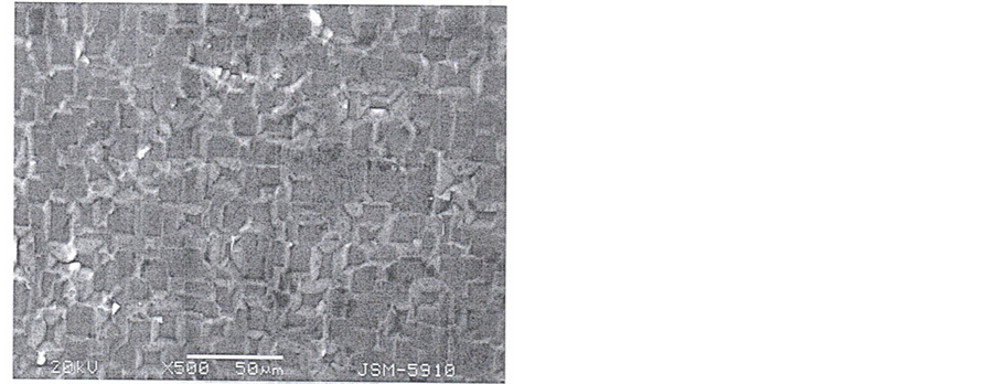
Micrographs of controlled samples Figure 2(a), depicts rectangular shaped grains arranged in a regular pattern with roughly same dimensions of the boundaries. Sides of each grain appear to be either 10 or 20 µm. Top surface of every grain represents (100) plane.
Micrograph of etched samples recorded at 2000 and 4000 magnifications, Figure 2(b) and Figure 2(c) show a modified surface after etching, which is different as compared to surface of the samples shown in Figure 2(a). Rectangular grains and boundaries have totally disappeared and instead circular dots appeared on the surface. Width of the boundaries and diameter of the dots is roughly 1 µm and 2 µm respectively. These dots appeared to be lined-up in two different directions at 90˚ or 45˚ to each other indicating etched planes in either (100) or (110) directions. Etching appeared to be uniform over a wide range of the surface, Figure 2(a). Images of the etched surface recorded at 120,000 magnification gives very interesting result about the size of the sub-features on the surface of the dots. Surface of every dot appears to be covered with very small sub dots (bright spots in the figure). Roughly 16 dark and bright spots line up in 0.1 µm that yield 5 nm diameter of each sub dot, now termed as quantum dots.
2.3. Surface Area and Pore Size Analyses
The surface area and pore size of the pores etched in silicon have been measured by surface area and pore size

Figure 1. Set for sample preparation.
 (a)
(a)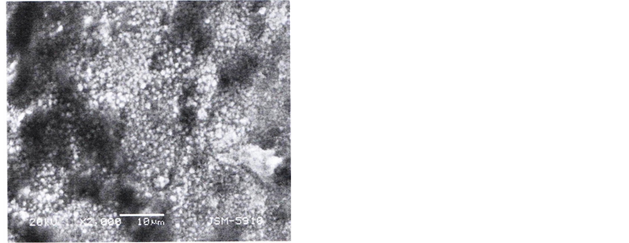 (b)
(b)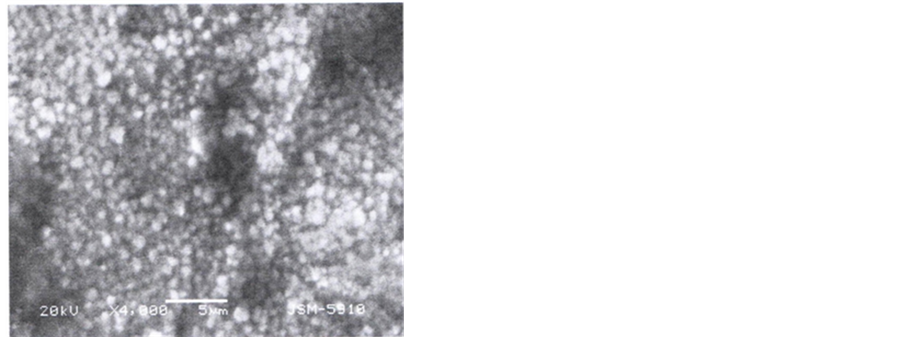 (c)
(c) (d)
(d)
Figure 2. (a): SEM image of control sample; (b): SEM image of etched sample at ×2000; (c): SEM image of etched sample at ×2000; (d) SEM image of etched sample at ×120,000.
analyzer (Following two figures have not been discussed).
The detail of measurements is given below. The relative pressure  has been measured and plotted against
  for unetched and etched samples. The plots of each sample are shown in Figure 3(a)Figure 3(b)). The porosity is measured from the slop of the best fit line through data points plotted in a graph as relative pressure
  verses
  for as grown and etched samples using following equations
[1] .
 where,
  and
and . Assuming pores are cylindrical, the following equation is valid for the pore radius.
 [20]
[20]
Pore radius calculated using above equations is roughly 6 nm.
The pore surface area, volume and diameter measured at relative pressure 2.94 × 10⁻² are listed below Surface area = 441.43 m2/g Pore value volume = 1.30 cc/g Pore diameter = 118.03 Å
Pore radius = 59 × 10−10 meter = 5.9 × 10⁻⁹ ≈ 6 nm.
 (a)
(a)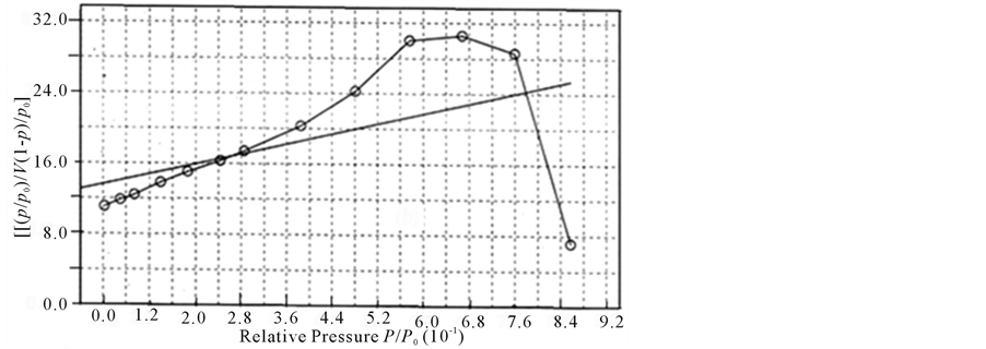 (b)
(b)
Figure 3. (a), (b): A plot  vs
vs  of control (a) and etched (b) samples.
2.4. Thermo Gravimetric/Differential Thermal Analysis
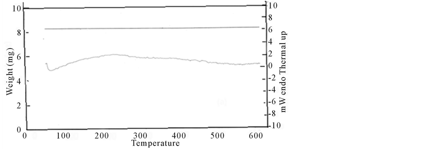
After performing above characterization, thermo gravimetric/differential thermal analysis (TG/DTA) has been carried out to study the porosity of etched silicon. During measurements change in weight of the samples as a function of temperature was recorded by increasing the temperature of the samples gradually up to 635˚C (temperature; high enough to force hydrogen related species to disappear) and change in weight against temperature was plotted Figure 3(a), Figure 3(b). The samples and an inert reference are made to undergo identical thermal cycles. During oxidation the reaction is endothermic or exothermic (heat flows in/out relative to the inert reference) was also recorded. TG/DTA thermograms {Figure 3(a), Figure 3(b)} depict both change in mass and amount of energy which are plotted on y axis against temperature. Thermograms (temperature from −24˚C to 635˚C) for un-etched (Figure 4(a)) show maximum endothermic and exothermic heat flow at about 50˚C and 200˚C respectively. The curve also shows that heat flow is dominantly exothermic in the range 100˚C to 635˚C (positive slope) and endothermic (negative slope) in the range −24˚C to 100˚C. However loss of weight per degree centigrade during reduction and gain during oxidation is not very high, which is not more than 10−4 mg/˚C. In the above description we have considered zero line as a reference where heat flow is 0 mW. But in our opinion rate of mass loss or gain and decrease or increase rate of heat energy indicate the dominance of endothermic or exothermic reactions, which means if the slope of a part of the curve is negative reduction is dominant and incase slope is positive oxidation is dominant.
Thermogram for etched samples shown in Figure 4(b) indicates that reduction of the sample continued dominantly up to 200˚C, (negative slope from 0˚C to 100˚C and positive slope in range 100˚C - 200˚C. This reduction reaction indicates a significant amount of hydrogen related species on the surface of etched samples. The reaction for the remaining part of temperature is exothermic, which high lights dominance of oxidation of the samples over reduction. Thermogram for etched samples can be divided into four regions I, II, III and IV. In region I slope of the thermogram is negative and reduction of the samples continued dominantly up to 100˚C with mass reduction rate 4.3 × 10⁻³ mg/˚C. Reduction peaks at 100˚C and later, oxidation started to compensate reduction that converts the slope of the thermogram to positive. The rate of weight gain is 2 × 10⁻³ mg/˚C. At 200˚C reduction and oxidation balance each other (heat flow in or out is zero). In regions II, III and IV reaction is exothermic and oxidation of the samples is dominant. In regions II, III and IV mass gain rates are 3 ×10⁻³ mg/˚C, 2 × 10⁻³ mg/˚C and 4 × 10⁻³ mg/˚C respectively which point out different oxidation reactions in these regions. To check the reactivity either endothermic or exothermic temperature range can also be divided into same four ranges. In range I (0˚C - 100˚C) endothermic reactivity is dominant that goes on increasing up to 100˚C and approach to maximum at 100˚C. Afterwards in range 100˚C to 200˚C exothermic reactivity plays its role, as a result endothermic reactivity starts decreasing and at about 200˚C endothermic and exothermic reactivthe thermogram is negative in this region. In the region 100˚C to 200˚C heat energy partially starts to flow out ity balances each other. The rate of heat (energy) flow in between (0˚C - 100˚C) is 0.062 mW/K, while slope of and compensate heat flow in. Endothermic reactivity decreases as a result, slope (mW/K = 0.02) of thermogram is positive. In regions II, III, and IV reaction is exothermic and rates of heat energy flow out are 0.022, 0.014 and 0.012 mW/K respectively. This result also supports our opinion of different reaction in regions II, III, and IV and formation of different oxygen related species on the surface of etched silicon.
 (a)
(a)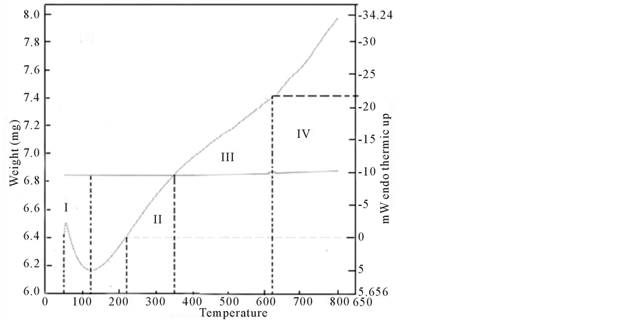 (b)
(b)
Figure 4. (a), (b): Thermogram of a control (a) and etched (b) samples.
3. Result and Discussion
The SEM image of the sample 1 given in Figure 2(a) clearly depicts the size and boundaries of the grains. SEM images of etched samples (Figure 2(b), Figure 2(c)) show that the grains can not maintain their regular rectangular shape, as exhibited by control samples, Figure 2(a). The difference in both surfaces indicates that a porous layer has been formed on the etched samples. The grain size appears to be of the order 1/2 µm radius and grain boundaries 1/4 µm. The dimensions are clear in micrograph scanned at 4000 magnification. Sub details of the grain surface highlighted at 120,000 magnifications (Figure 2(c) demonstrate that the surface of each dot is covered with quantum dots of diameter ~8 nm. Diameter of pores recorded by Pore size analyzer is also of the same order. The radius is of the pores and quantum dots are of the order of the atomic dimensions. Electron or hole confinement may give rise to energy states in the band gap of the quantum dots which is responsible for the emission of visible light from the surface of the etched silicon. It is still a question to the scientist whether the emission is from the layer of chemical species formed at the surface or quantum dots/quantum wires of silicon. The different chemical reactions observed during TG/DTA measurements in regions I, II, III, and IV high lights the presence of different species on the surface. The chemistry of reaction on the surface during etching is as follows [21] : when sample surface is fully covered with HF acid, the oxide dissolves and the surface becomes terminated with H atoms. The relative strength of bonds is as under: Si-H < Si-O < Si-F.
But Si-F bonds are highly polarized due to the large electro-negativity of fluorine and reaction following different paths and at the end of an HF etch, porous silicon samples contain primarily Si-H, SiH2, and SiH3 surface groups with minor concentration of O or F related species [21] .
Three exothermic reactions, which were apparently caused by the oxidation reaction observed in regions I, II, III, and IV, are related to Si-O bonds.
Keeping in view the relative bond strength of different species formed at the surface, given above, Arita et al. [22] have analyzed that Si-Si bond is weak as compared to Si-O bonds at higher temperatures, 300˚C to 635˚C. Si-Si bond easily changes into Si-O bond with the increase in temperature i.e. oxidation. Oxidation reaction on the surface in regions I, II, III, and IV follow different paths that also indicates the formation of a layer due different Hydrogen, oxygen and Fluorine related chemical species. In our opinion both layer of chemical species and quantum dots/wires can produce luminescence but wave length of the luminescence will be different which solely depends upon the energy states (due to quantum confinement) induced in the band-gap of the materials. Kabbi et al. [9] have also formed the openion that Quantum confinement and surface passivation are responsible for the electronic states of the silicon nano crystallites. Quantum dots and pore size appearing on the etched surface is of the order of nA and passivated surface may be of the order of Bohr Radius. Therefore, red emission appears to be the result of hole (material is p-type) confinement in the passivated layer.
4. Conclusion
The dimensions of pore size and quantum dots observed on the surface of HF vapor etched silicon are of the order of nanometer. The samples after etching exhibits red emission under UV light. The dimensions of these nanostructures (pores and quantum dots) suggest that emission of red luminescence is due to energy states induced by quantum confinment of electronsor holes which are noticed by scanning electron microscopy, and pore size analysis.
Acknowledgements
We acknowledge Govt. Denny’s Higher Secondary School for providing space to perform chemical reaction Rawalpindi, Pakistan and Central research Laboratory Peshawar University, Peshawar Dr. Said Karim Shahawar, Pakistan for measurements/characterization of the samples on payment.
References
- Kumar, P., Lemmens, P., Ghosh, M., Ludwig, F. and Schilling, M. (2009) Effect of HF Concentration on Physical and Electronic Properties of Electrochemically Formed Nanoporous Silicon. Journal of Nanomaterials, 18, Article ID: 727957, 7 p.
- Abramof, P.G., Beloto, A.F., Ueta, A.Y. and Ferreira, N.G. (2006) X-Ray Investigation of Nanostructured StainEtched Porous Silicon. Journal of Applied Physics, 99, Article ID: 024304.
- Anderson, O.K. and Veje, E. (1996) Experimental Study of the Energy-Band Structure of Porous Silicon. Physical Review B, 53, 15643-15652. http://dx.doi.org/10.1103/PhysRevB.53.15643
- Wallacher, D., Künzner, N., Kovalev, D. and Knorr, N. (2004) Capillary Condensation in Linear Mesopores of Different Shape. Physical Review Letters, 92, Article ID: 195704.
- Hirschman, K.D., Sybeskov, L.T., Dittagupta, S.P. and Fauchet, P.M. (1996) Silicon-Based Visible Light-Emitting Devices Integrated into Microelectronic Circuits. Nature, 384, 338-341. http://dx.doi.org/10.1038/384338a0
- Streimer, C.C., Gaborski, T.R., McGrath, J.L. and Fauchet, P.M. (2007) Chargeand Size-Based Separation of Macromolecules Using Ultrathin Silicon Membranes. Nature, 445, 749-753. http://dx.doi.org/10.1038/nature05532
- Föll, H., Carestensen, J. and Frey, S. (2006) Porous and Nanoporous Semiconductors and Emerging Applications. Journal of Nanomaterials, 2006, Article ID: 91635.
- Kumar, P. and Huber, P. (2007) Nucleation and Growth of Copper on Mesoporous Silicon by Immersion Plating. Journal of Physics D: Applied Physics, 40, 2864-2869. http://dx.doi.org/10.1088/0022-3727/40/9/030
- Kabbi, H., Miliki, N., Cheynet, M., Saikalay, W., Gibbert, D., Bassїs, B., Yangui, B. and Charї, A. (2006) Structural and Optical Properies of Vapour-Etching Based Porous Silicon. Crystal Research and Technology, 41, 154-162.
- Kore, L. and Bosman, G. (1999) Feasibility of Porous Silicon as a Primary Material in Solar Cells. Solar Energy Materials and Solar Cells, 57, 31-48.
- Bastide, S., Mcuniot, P., Williams, N., Le, Q., Sarti, D. and Levy-Clement, C. (1994) The Effect of Porous Silicon on the Emitterr of Photovoltaic Cell. Proceedings of 12th European Photovoltaic Solar Cell conference, Amsterdam, April 11-15, 1994, 780.
- Aouida, S., Saadoum, M., Saad, K.B. and Bessaїs, B. (2006) Phase Transition and Luminescence Properties from Vapor Etched Silicon. Thin Solid Films, 495, 357-3609. http://dx.doi.org/10.1016/j.tsf.2005.08.235
- Canham, L.T. (1990) Silicon Quantum Wire Array Fabrication by Electrochemical and Chemical Dissolution of Wafers. Applied Physics Letters, 57, 1046. http://dx.doi.org/10.1063/1.103561
- Khitaryan, Z.H.M., Aroutiounian, V.M. and Durgaryan, A.A. (2010) Influence of Temperature on Current Voltage Characterisics and Noise of Hydrogen Sensors. Sensors and Transducers Journals, 117, 106-111.
- Koropecki, R.R., Arce, R.D. and Schmidt, J.A. (2004) Infrared Studies Combined with Hydrogen Effusion Experiments on Nanostructured Porous Silicon. Journal of Nano-Crystalline Solids, 338-340, 159-162.
- Chen, S.Y., Kashkarov, P.K., Timoshenko, V.Y., Liu, B.L. and Jiang, B.X. (2003) Characterization and Luminescence Properies of Annealed Poroussilicon. Journal of Crystal Growth, 247, 446-451.
- Tischler, M.A., Collins, R.T., Stathis, J.H. and Tsang, J.C. (1992) Luminescence Degradation in Porous Silicon. Applied Physics Letters, 60, 639. http://dx.doi.org/10.1063/1.106578
- Elhouichet, H., Bessais, B., Ben younes, O., Ezzaouia, H. and Oueslati, M. (1997) Changes in Photoluminescence Behaviour and Structure of Porous Silicon Related to Preparation Conditions and Laser Irradiation. Thin Solid Films, 304, 358-368. http://dx.doi.org/10.1016/S0040-6090(97)00091-6
- Cullis, A.G., Canham, L.T. and Calcott, P.D.J. (1997) The Structural and Luminescence Properties of Porous Silicon. Journal of Applied Physics, 82, 909. http://dx.doi.org/10.1063/1.366536
- Baklanov, M.R., Mogilnikov, K.P., Polovinkin, V.G. and Dultsev, F.N. (2000) Determination of Pore Size Distribution in Thin Films by Elipsometric Porosimetry. Journal of Vacuum Science and Technology, B18, 1385 p.
- Boonekamp, E.P., Kelly, J.J., van de Ven, J. and Sondag, A. (1994) The Chemical Oxidation of Hydrogen-Terminated Silicon (111) Surfaces in Water Studied in Situ with Fourier Transform Infrared Spectroscopy. Journal of Applied Physics, 75, 8121. http://dx.doi.org/10.1063/1.356510
- Arita, Y., Kuranari, K. and Sunohara, Y. (1976) Thermal Behavior of Porous Silicon. Japanese Journal of Applied Physics, 15, 1655-1664. http://dx.doi.org/10.1143/JJAP.15.1655