Journal of Surface Engineered Materials and Advanced Technology
Vol.3 No.1(2013), Article ID:27329,5 pages DOI:10.4236/jsemat.2013.31006
Role of Substrate Temperatures on Structural, Optical, Wetting and Electrical Transport Properties of CdS Thin Films
![]()
Materials Research Laboratory, Department of Physics, Ahmednagar College, Ahmednagar, India.
Email: drpravinmore@gmail.com
Received September 20th, 2012; revised October 20th, 2012; accepted October 25th, 2012
Keywords: CdS Thin Film; Spray Pyrolysis; Band Gap; Contact Angle
ABSTRACT
Cadmium sulphide thin films were deposited on the glass substrate via simple spray pyrolysis technique. The substrate temperatures (Ts) have been varied from 250˚C to 350˚C and concentration of precursor’s solution of cadmium chloride and thiourea was optimized. The X-ray patterns and morphological studies of CdS thin films indicated that films are crystalline in nature with hexagonal crystal structure. The grain size calculated and found to be 250.12 to 349.61 nm. The optical spectra exhibited high transmittance and band gap varied from 2.41 eV to 2.39 eV. The angle of contact measured and found to be hydrophilicity behaviour. The electrical conductivity and thermoelectric power have been measured with two probe method. It was found that CdS thin films were semiconducting in nature with n-type.
1. Introduction
The use of semiconducting materials in the form of thin films now a day’s occupy prominent place in the basic as well as applied research. It is a technologically useful material due to wide band gap of 2.42 eV, as many devices such as electronic devices including light emitting diodes, single electron transistors and field effect transistor [1] sensors [2] window materials [3]. CdS solar cell has several years been considered to be a promising alternative to the more widely used silicon devices [4]. The efficiency and performance of the devices depends on the optical and electrical properties of the thin films. So that attempt tried to understand the role of substrate temperatures on structural, optical, wetting and electrical transport properties of CdS thin films.
Thin film of CdS has been prepared by several methods including Vacuum [5] sputtering [6] spray pyrolysis [7,8] chemical bath deposition [9]. The interest to nonvacuum methods for thin films deposition has increased. The solution based processes have several advantages viz: simplicity of process, precise composition, applicability to substrates of any size. These are important for practical applications. The SPD meets practically all the requirements to the methods for the films deposition on large substrate [10].
2. Methodology
Cadmium sulphide thin films were deposited via spray pyrolysis technique using aqueous solution of cadmium chloride (CdCl2 of 0.1 M) and thiourea (NH2CSNH2 of 0.2 M) at 250˚C, 300˚C and 350˚C substrate temperatures. The substrate was cleaned by ultrasonic cleaner. The samples were deposited by spraying 30 ml prepared solution at the rate of 5 ml/min using air as a carrier gas. The nozzle to substrate distance was kept around 22 cm.
The structural properties of CdS studied by X-ray diffraction (XRD) using filtered CuKα radiation (λ = 1.5406 Å). The surface morphologies of the CdS thin films carried out by scanning electron microscope operating at 25 KV. The optical studies carried in the range of 300 - 950 nm wavelengths. Contact angle of CdS were measured using standard goniometer (Ramehart Instrument Co., USA) equipped with CCD camera.
3. Results and Discussion
3.1. X-Ray Diffraction Studies
X-ray diffraction patterns of CdS films deposited at 250˚C, 300˚C and 350˚C substrate temperatures as shown in Figure 1. It is observed that XRD pattern showed preferential orientations along (100), (002) and (101) additionally (110), (103) and (201) directions. All the diffraction peaks can be indexed to a hexagonal structured. No obvious characteristic diffraction peaks from other impurities can be detected. From XRD studies it is clear that the intensity of peaks is function of substrate temperature and suggests that as deposited CdS films are crystalline
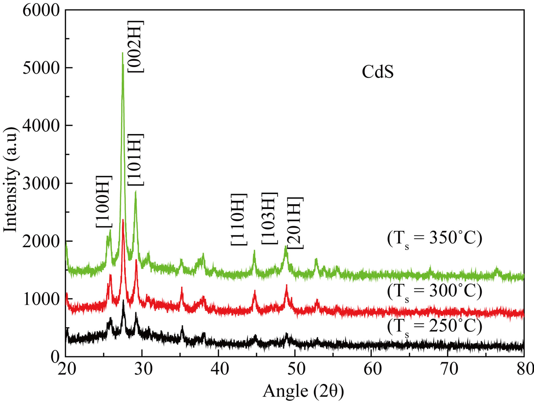
Figure 1. X-ray diffraction patterns of CdS thin films as a function of substrate temperatures.
in nature which is similar to reported in the literature [7,8].
Figure 2 shows the variation in intensity. The lattice parameters were calculated from the XRD data and are found to be close agreement with the JCPD data [11]. The grain size were calculated at q = 27.55˚ by using Scherer’s relation and listed in Table 1.
 (1)
(1)
where, l-wavelength, b-broadening of diffraction line measured at half maximum intensity and q-angle.
The dislocation density (δ) was evaluated by the formula [12].
 (2)
(2)
3.2. Compositional Studies
The EDX analysis carried out to study the composition of films in the binding energy region between 0 to 20 keV, shown in Figure 3. The EDX spectrum of CdS thin films exhibits clear existence of Cd and S elements with stoichiometric ratio.
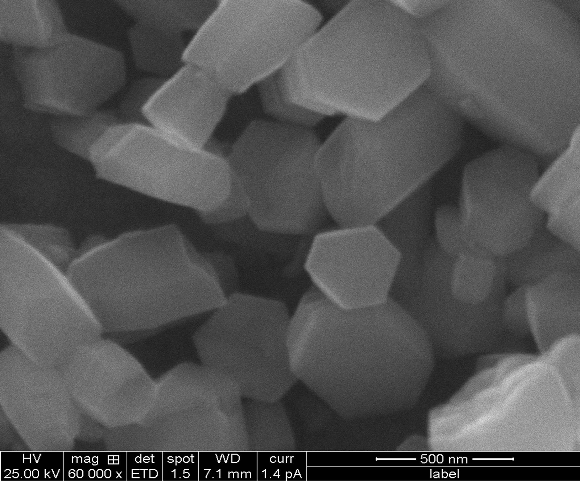
3.3. Surface Morphology Studies
SEM is one of the most useful and versatile technique for the investigation of surface topography, microstructural features etc. because such properties of films influence their optical study. Figure 4 shows surface morphology of CdS thin films. Thin films of CdS found homogeneous, well adherent and cover the glass substrate without cracks and pinholes. The surface morphology shows well developed hexagonal structure.
3.4. Optical Studies
The optical spectra’s of as deposited CdS thin films were
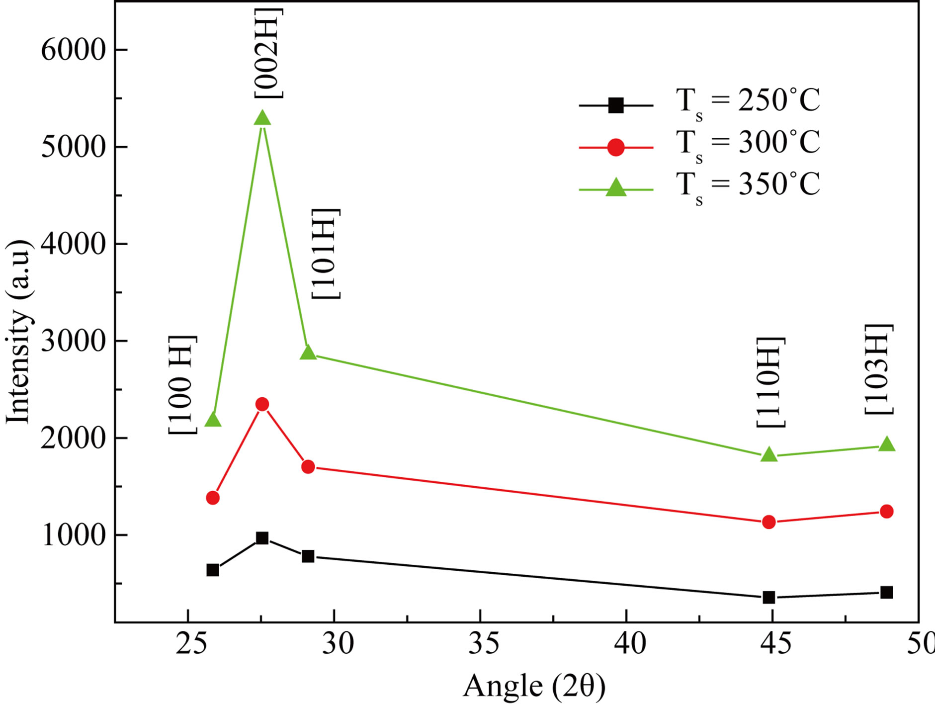
Figure 2. Variation in intensity of CdS thin films.
Table 1. The band gap (Eg), refractive index (n), static dielectric constant (eo), dislocation density (d) grain size and contact angle as a function of substrate temperatures.
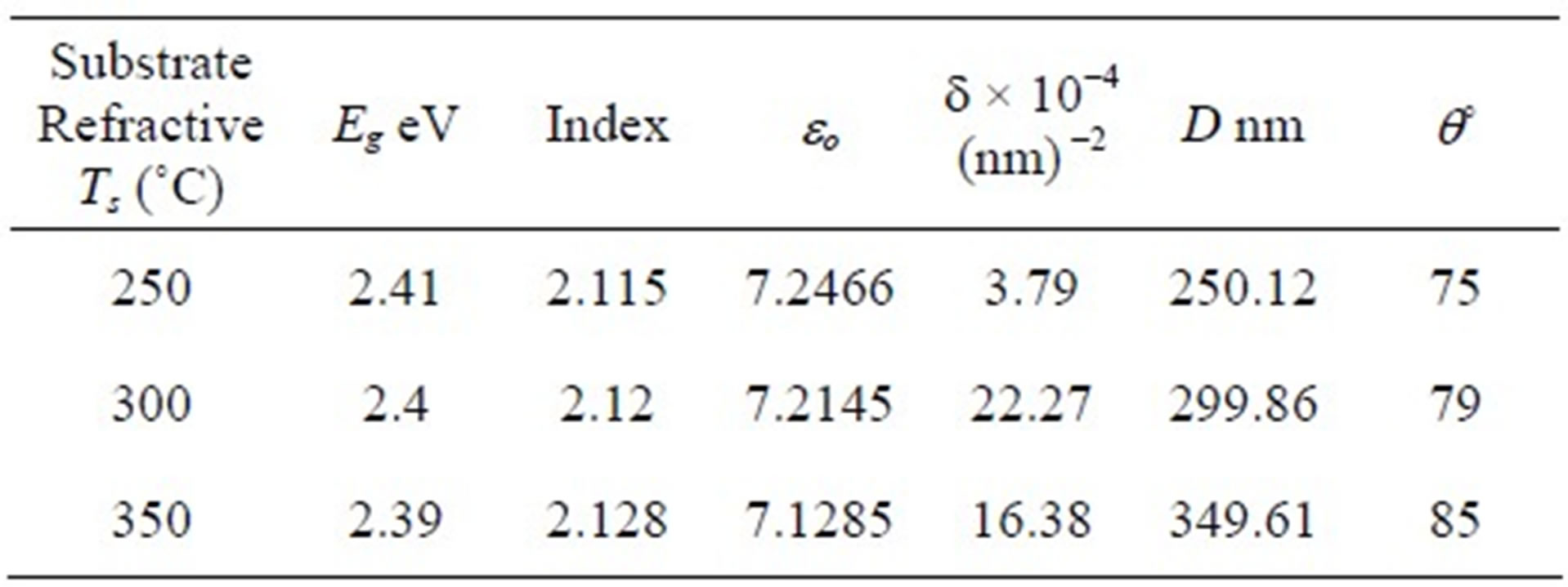
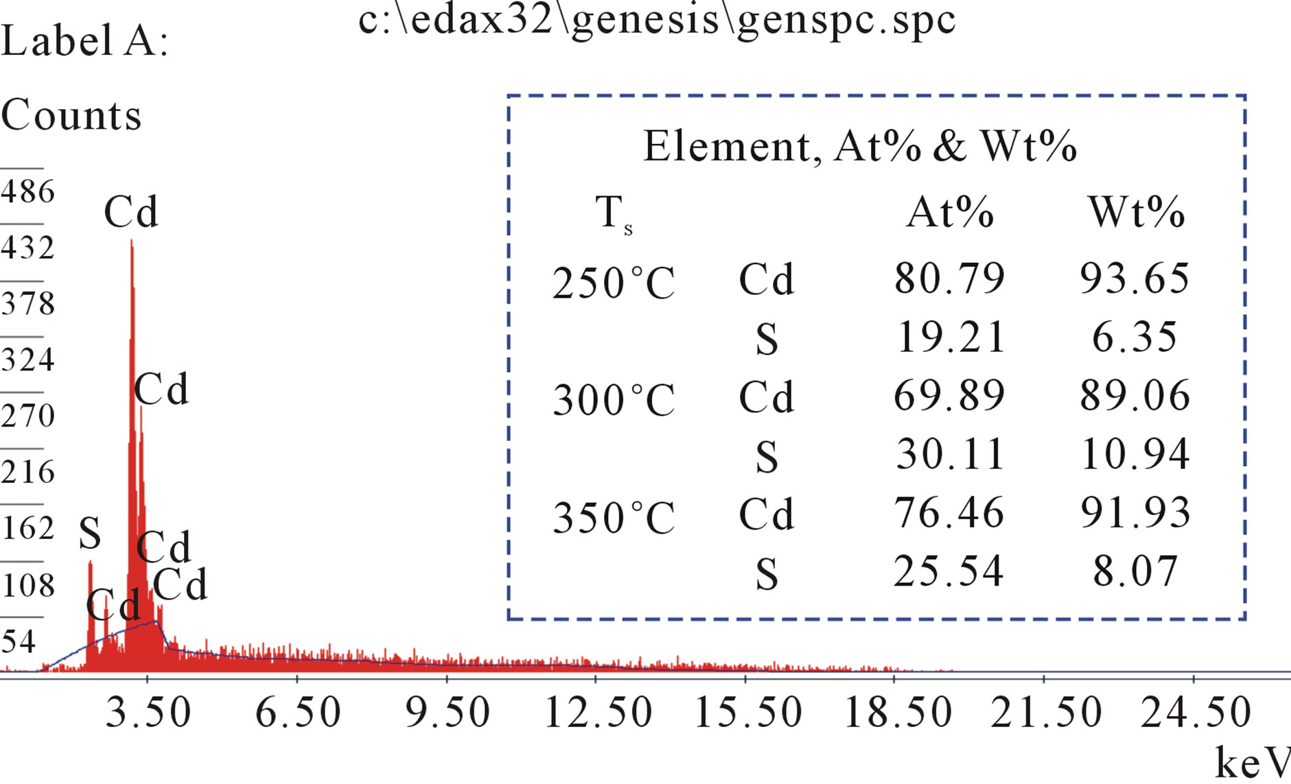
Figure 3. EDX of CdS thin films at Ts = 250˚C.
recorded by UV-VIS double beam spectrophotometer in the range of 300 - 950 nm at room temperature. Figure 5 shows the variation of optical transmittance with wavelength. The optical study shows that the films are absorptive. The value of absorption coefficient is depending upon radiation energy as well as the composition of films. The optical band gaps of the CdS films are found to decrease (from 2.41 eV to 2.39 eV) with increase in substrate temperatures shown in Figure 6. This is due to the increase of grain size on increase in substrate temperatures [7]. The plots of (αhν)2 vs hν are linear in high energy region indicating direct type of transitions in these
 (a)
(a)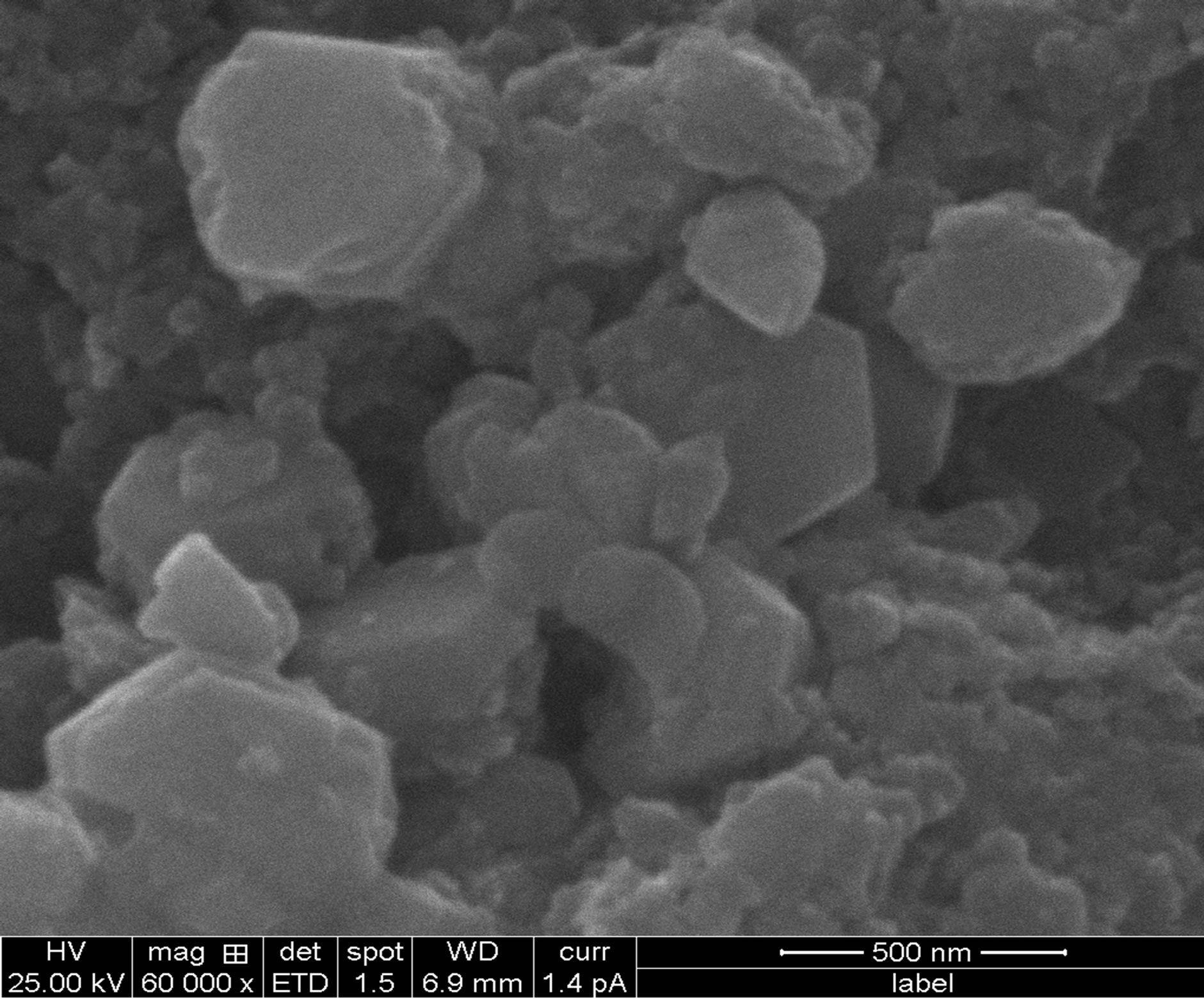 (b)
(b)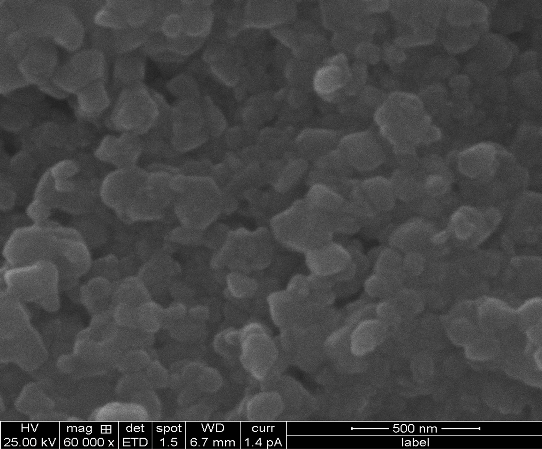 (c)
(c)
Figure 4. Indicate the temperature SEM (a) Ts = 250˚C (b) Ts = 300˚C (c) Ts = 350˚C.
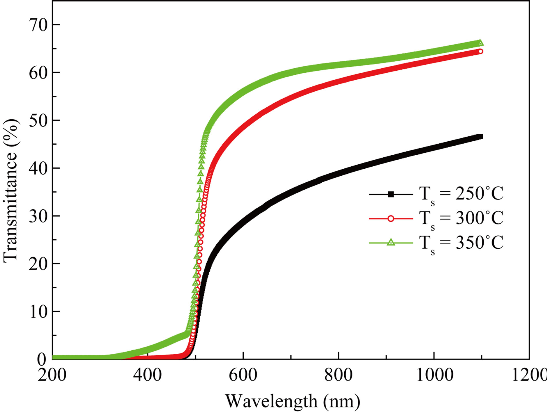
Figure 5. Optical transmittance of CdS thin films different substrate temperatures.
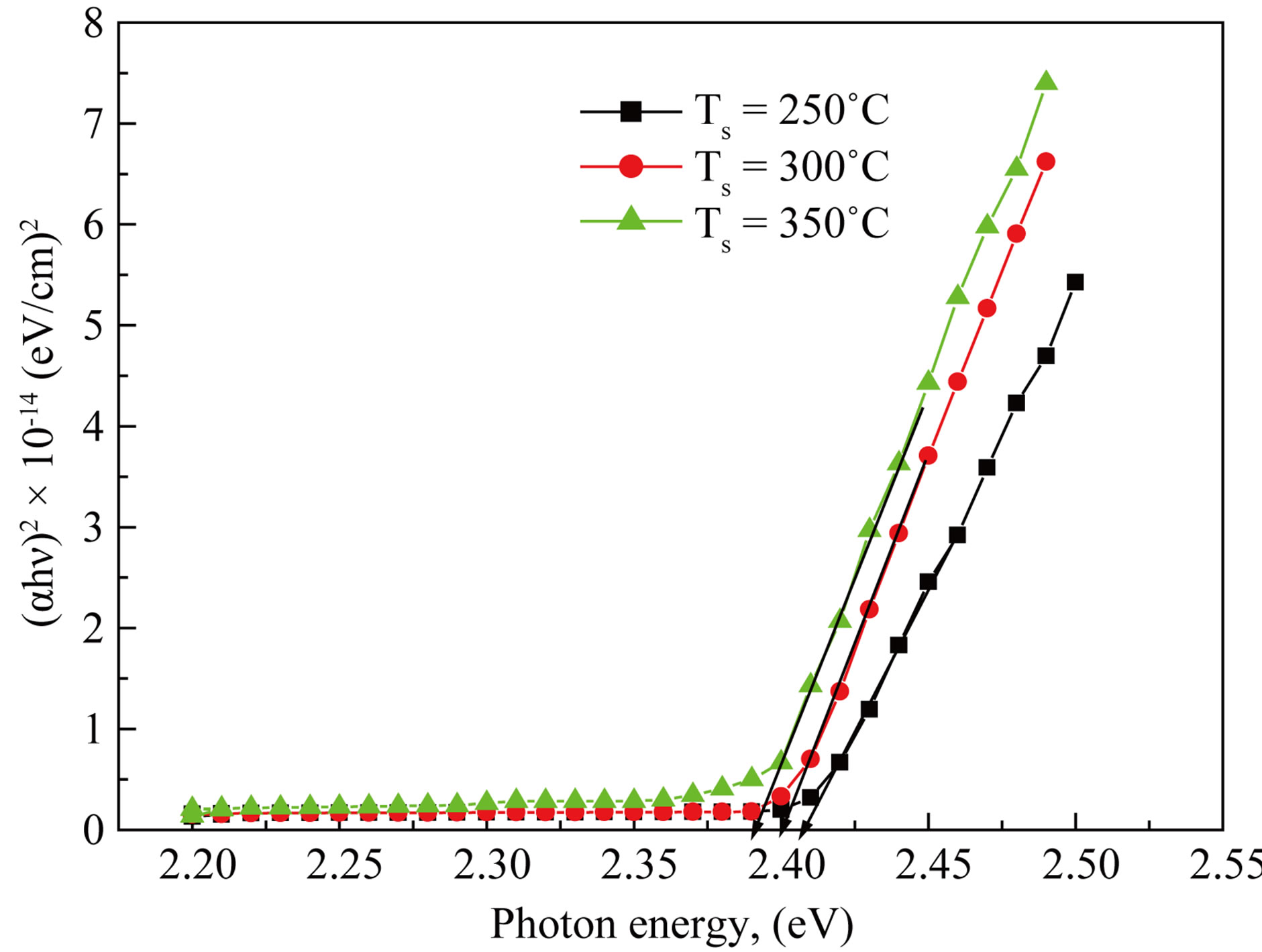
Figure 6. Optical band gap determination of CdS thin films as a function of substrate temperatures.
films. The type transition was also confirmed by considering the following relation [9,13]
 (3)
(3)
where symbols have their usual meanings and m = 0.5 for allowed direct and m = 3/2, 2 and 3 for other transtion.
The refractive index calculated from the following relation presented by Ravindra et al. [12]
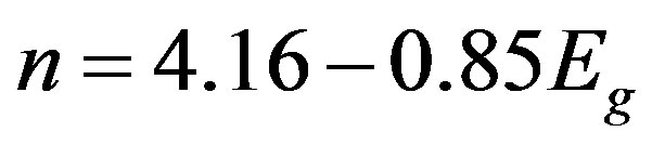 (4)
(4)
The static dielectric constant (εo) of the films calculated using a relation expressing the energy band gap dependence of εo for semiconductor in the following form [12].
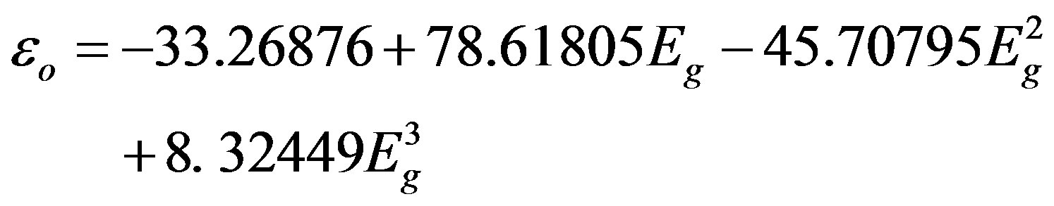 (5)
(5)
3.5. Wetting Studies
Wetting refers to the study of how a liquid deposited on a solid (or liquid) substrate spreads out. Spreading parameter, S measures by following relation.
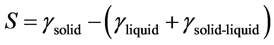 (6)
(6)
The wetting of solid with water is dependent on the relation between the interfacial tensions. The ratio between water/air, water/solid and solid/air determines the contact angle between a water and droplet on a given surface. Measurement of surface water contact angle is inversely proportional to the wettability and can be determined by Young-Dupre relation [14].
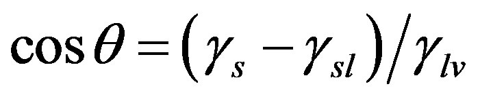 (7)
(7)
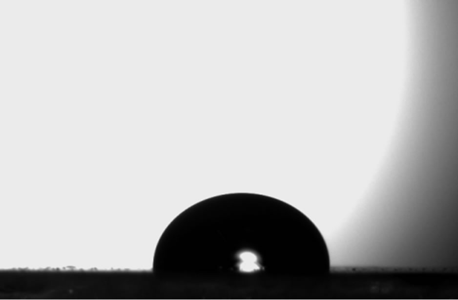
From the Figure 7 it is clear that contact angle is temperature dependent phenomenon and indicating hydrophilic behaviour (θ < 90˚) means the solid has a high affinity for water.
3.6. Electrical Studies
DC Conductivity
The conductivity of CdS thin films were measured by two probe method. The variation of dc conductivity with reciprocal temperature (1000/T) is depicted in Figure 8" target="_self"> Figure 8. It was found that conductivity increases with increasing substrate temperatures. The higher values of conductivity may be due to higher crystallanity [2]. It shows semiconducting nature of the material. Further it is observed that conductivity obeys Arrhenius behavior indicating a semiconducting transport behavior. It is seen that there are two distinct conducting regions indicating more than one conduction mechanisms due to the localized states responsible for this conduction process are the direct
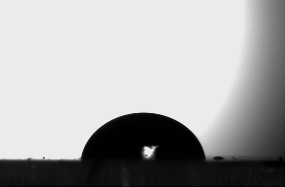
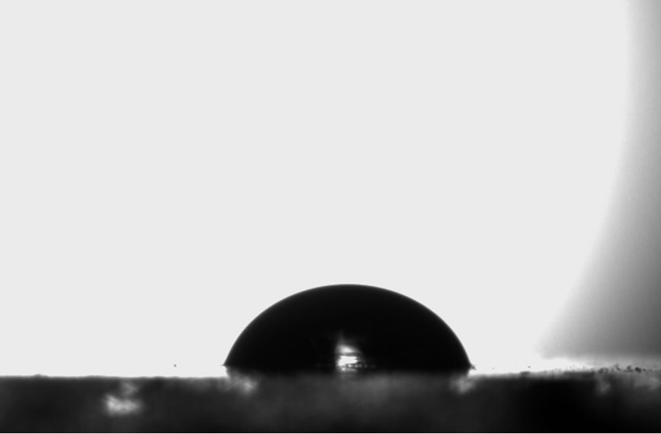
Ts = 250˚C Ts = 300˚C
Ts = 350˚C
Figure 7. Contact angle measurement of CdS thin films at different substrate temperatures.
consequence of the imperfections associated with thin films [15]. The activation energies were calculated using the relation.
 (8)
(8)
where, s is the conductivity at temperature T, so is a constant, K is the Boltzmann constant, T is the absolute temperature and Ea is the activation energy. The activetion energy represents the location of trap levels below the conduction band. It is seen that the activation energy (HT) is increases from 0.30 to 0.568 eV.
3.7. Thermoelectric Power
The thermoemf of CdS thin films were measured as a function of temperature in the range 300 - 500 K. The polarity of the thermally generated voltage at the hot end was positive, indicating that the CdS thin films are of n-type [16]. The variation of the thermoemf (∆V) with temperature is shown in Figure 9. The thermoemf in-
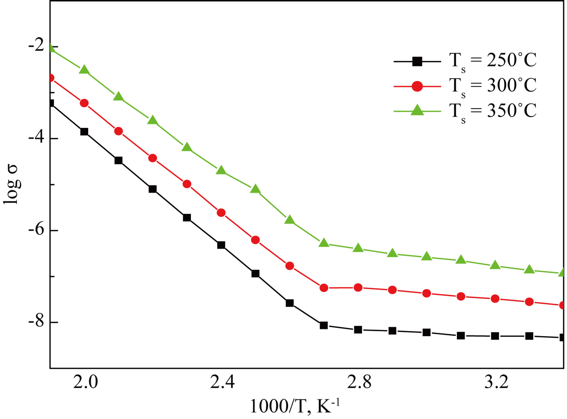
Figure 8. Variation of the dark electrical conductivity with inverse absolute temperature.
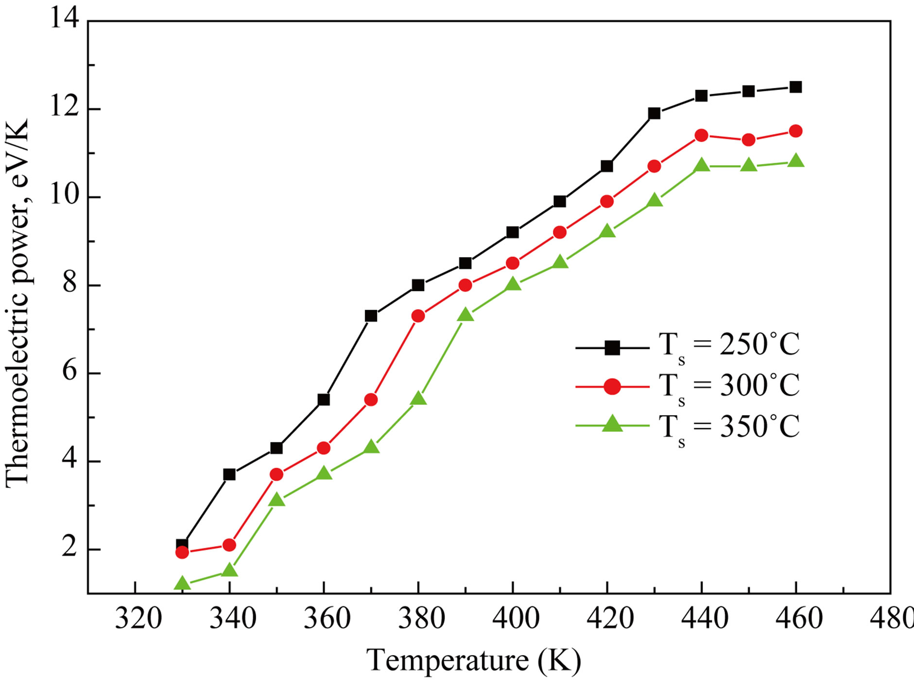
Figure 9. Variation in thermoelectric power with substrate temperatures.
creases with increasing temperature.
4. Conclusion
Role of substrate temperatures on CdS thin films were studied successfully by spray pyrolysis technique. XRD studies showed that the sharpness of peaks were function of substrate temperatures and suggested that as deposited CdS films were crystalline in nature. The optical properties showed films were smooth, free from pin hole with around 70% transmittance. The optical band gap varied in the range of 2.41 - 2.39 eV due to change in grain size with respect to substrate temperatures. The contact angle varies with substrate temperatures and showed hydrophilic in nature. The electrical studies revealed that the conductivity of CdS increases with substrate temperatures as well as working temperature, confirming semiconducting in nature. TEP of CdS films increases with both temperatures.
REFERENCES
- Y. Ni, H. Liu, F. Wang, Y. Liang, J. Hong, X. Ma and Z. Xu, “PbS Crystal with Clover like Structure: Preparation, Characterization, Optical Properties and Influencing Factors,” Crystal Research and Technology, Vol. 39, No. 3, 2004, pp. 200-206.
- K. M. Garadkar, A. A. Patil, P. V. Korake and P. P. Hankare, “Characterization of CdS Thin Films Synthesized by SILAR Method at Room Temperature,” Archives of Applied Science Research, Vol. 2, No. 5, 2010, pp. 429-437.
- N. I. Achuko and C. C. Ugwuegbu, “Optical Properties of CdS Thin Films Obtained by Chemical Bath Deposition,” International Journal of Academic Research, Vol. 6, 2011, pp. 368-374.
- J. Barman, J. P. Borach and K. C. Sarma, “Effect of pH Variation on Size and Structure of CdS Nanocrystalline Thin Films,” Chalcoginide Letters, Vol. 11, No. 5, 2008, pp. 265-266.
- K. K. Singh, M. Kar and H. L. Das, “Effect of Substrate Temperature on Photoconductivity in CdS Thin Films,” Indian Journal of Pure & Applied Physics, Vol. 48, No. 2, 2010, pp.110-114.
- S.-G. Hur and E.-T. Kim, J.-H. Lee, G.-H. Kim and S.-G. Yoon, “Characterization of Photoconductive CdS Thin Films Prepared on Glass Substrates for Photoconductive Sensor Applications,” Journal of Vacuum Science & Technology B, Vol. 26, No. 4, 2008, pp.1334-1337. doi:10.1116/1.2945301
- A. Ashour, “Physical Properties of Spray Pyrolysed CdS Thin Films,” Turkish Journal of Physics, Vol. 27, No. 6, 2003, pp. 551-558.
- C. S. Tepantlan, “Structural, Optical and Electrical Properties of CdS Thin Films by Spray Pyrolysis,” Revista Mexcana de Fisica, Vol. 54, No. 2, 2008, pp. 112-117.
- J. Barman, K. C. Sarma, M. Sarma and K. Sarma, “Structural and Optical Studies of Chemically Prepared CdS Nanocrystalline Thin Films,” Indian Journal of Pure and Applied Physics, Vol. 46, 2008, pp. 339-343.
- D. Todorvsky, R. Todorvsky, N. Petrova, M. U. Bojnova and M. Milanova, “Spray-Pyrolysis, Deepand Spin-Coating Deposition of Thin Films and Their Characteristics,” Journal of the University of Chemical Technology and Metallurgy, Vol. 41, No. 1, 2006, pp. 93-96.
- JCPD Card No. 75-1545.
- Y. Akaltun, M. A. Yildirım, A. Ates and M. Yildirim, “The Relationship between Refractive Index-Energy Gap and the Film Thickness Effect on the Characteristic Parameters of CdSe Thin Films,” Optics Communications, Vol. 284, 2011, pp. 2307-2311.
- P. D. More, G. S. Shahane, L. P. Deshmukh and P. N. Bhosale, “Spectro-Structural Characterisation of Cd (Se, Te) Alloyed Thin Film,” Materials Chemistry and Physics, Vol. 80, 2003, pp. 48-51.
- D. P. Dubal, D. S. Dhawale, R. R. Salunkhe, S. M. Pawar, V. J. Fulari and C. D. Lokhande, “A Novel Chemical Synthesis of Interlocked Cubes of Hausmannite Mn3O4 Thin Films for Supercapacitor Application,” Journals of Alloys and Compounds, Vol. 848, 2009, pp. 218-221.
- P. D. More and L. P. Deshmukh, “Electrical Conduction in Chemically Deposited CdSe1-xTex Mixed/Alloyed Thin Films,” Indian Journal of Engineering and Materials Sciences, Vol. 10, 2003, pp. 427-432.
- S. L. Patil, M. A. Chougule, S. G. Pawar, B. T. Raut, S. Sen and V. B. Patil, “New Process for Synthesis of ZnO Thin Films: Microstructural, Optical and Electrical Characterization,” Journal of Alloys and Compounds, Vol. 509, No. 41, 2011, pp. 10055-10061.