Journal of Crystallization Process and Technology
Vol.3 No.1(2013), Article ID:27292,13 pages DOI:10.4236/jcpt.2013.31006
Structural, Morphological, Optical and Electrical Properties of Zn(1−x)CdxO Solid Solution Grown on aand r-Plane Sapphire Substrate by MOCV
![]()
1Laboratory of Physical Chemistry Materials, USCR “High Resolution X-Ray Diffractometer”, Department of Physics, Faculty of Sciences of Monastir, University of Monastir, Monastir, Tunisia; 2Research Unit of Heteroepitaxy and Its Applications, Department of Physics, Faculty of Sciences of Monastir, University of Monastir, Monastir, Tunisia; 3Laboratory of Physical Chemistry Interfaces, Department of Physics, Faculty of Sciences of Monastir, University of Monastir, Monastir, Tunisia; 4Group Study of Condensed Matter, CNRS/University of Versailles Saint Quentin en Yvelines, Paris, France.
Email: *Fouzri.Afif@gmail.com
Received August 18th, 2012; revised September 25th, 2012; accepted October 8th, 2012
Keywords: II-VI Material; Zn(1−x)CdxO Solid Solutions; Metal Organic Chemical Vapor Deposition; High Resolution X-Ray Diffraction; Atomic Force Microscopy; Scanning Electron Microscopy; Photoluminescence; Hall Mobility
ABSTRACT
Zn(1−x)CdxO films have been grown on  (a-plane) and
  (r-plane) sapphire substrate by metal organic chemical vapor deposition. A maximum cadmium incorporation of 8.5% and 11.2% has been respectively determined for films deposited on aand r-plane sapphire. The optical transmission spectra and energy band-gap equation established by Makino et al. were used to estimate the cadmium mole fraction of the solid solutions. Structural, morphological and optical properties of these films were examined using high resolution X-ray diffraction (HRXRD), atomic force microscopy (AFM) and room and low temperature photoluminescence (Pl) as Cd incorporation and employed substrate. X-ray diffraction study revealed that all films had wurtzite phase but solid solution grown on a-plane sapphire are polycrystalline with a preferred orientation along the [0001] direction and a-plane
  film are epitaxially grown on r-plane sapphire. AFM image show significant differences between morphologies depending on orientation sapphire substrate but no significant differences on surface roughness have been found. The near band-edge photoluminescence emission shifts gradually to lower energies as Cd is incorporated and reaches 2.916 eV for the highest Cd content (11.2%) at low temperature (20 K). The room temperature hall mobility decreases with the Cd incorporation but it is larger for Zn(1−x)CdxO grown on r-plane sapphire.
1. Introduction
As a direct wide-band-gap semiconductor, ZnO has received increasing attention due to its potential applicability to optoelectronic devices such as ultraviolet (UV)- light emitting diodes (LEDs) and laser diodes (LDs) [1,2]. Since the first reports on ZnO-based heterostructures the issue of band gap engineering, as a means to control the actual device emission energy, was addressed [3-6]. ZnO has an ability to modulate the band gap to lower level by alloying with CdO [7]. The growth of both solid solutions presents the difficulty of combining materials with different crystalline structures, on the one hand hexagonal ZnO and then cubic CdO. Thus, the achievement of high Cd concentrations represents a challenge for crystal growers, since these growth problems lead to phase separation.
Most of the studies deal with c-plane oriented thin films. However, devices based on [0001]-oriented wurtzite materials are known to present spontaneous and piezoelectric electrostatic fields which spatially separate electrons and holes in the active layers and, thus, limit the device quantum efficiency [8]. Therefore, alternative growth orientations have been recently proposed with the polar [0001] direction within the growth plane [9,10] and quantum wells (QWs) free of electric fields have already been demonstrated [9-11].
In this paper, we analyze the structural, morphological, optical and electrical properties of Zn(1−x)CdxO solid solution grown by metal organic chemical vapor deposition (MO-CVD) on  and
and  -plane sapphire. The effect of increasing Cd concentration on the optical properties of the films has been evaluated by photoluminescence (Pl), while high-resolution X-ray diffracttion (HRXRD), atomic force microscopy (AFM) has been used to analyze the structural properties and morphology of Zn(1−x)CdxO layers as function of cadmium concentration. The electrical property was investigated by Van der Pauw Hall measurements at room temperature.
2. Experimental Details
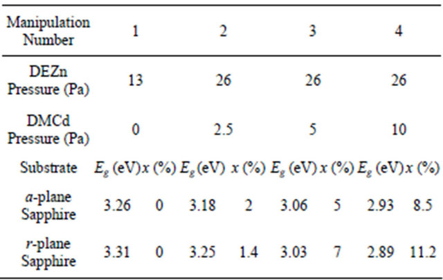
The layer is grown in horizontal MO-CVD reactor at atmospheric pressure under N2 carrier gas. Diethyl-Zinc (DEZn), Dimethyl-Cadmium (DMCd) and tertiary butanol (ter-butanol) are used as Zn, Cd and oxygen precursors, respectively at a growth temperature of 380˚C. The growth conditions are described elsewhere [12]. With similar growth parameters, thin films of Zn(1−x)CdxO are directly deposited on aand r-plane sapphire substrates from Crystec. The cadmium incorporation is obtained by using different flux ratios between DMCd and DEZn while the DEZn partial pressure is kept constant. The growth parameters of two series of four samples are listed in Table 1. We will note in the following, the first series of solid solution deposited on a-plane sapphire substrate by MSAi and the second series deposited on r-plane sapphire substrate by MSRi, where i is the manipulation number.
Thickness of ZnCdO film deposited on aand r-plane sapphire substrate are respectively about 2.8 µm and 2.2 for MSA4 and MSR4 (Figure 1). They clearly show
Table 1. MOCVD growth parameters, energy band gap (Eg) and cadmium concentration at % of Zn(1−x)CdxO solid solutions deposited on aand r-plane sapphire substrate.
the non-uniformity of layers thickness. These samples are characterized by optical transmission measurements in the range 360 - 690 nm using a DR/4000U spectrophotometer which can return either the absorption coefficient or the transmittance in percentage.
HRXRD experiments were performed with D8 discover Bruker AXS diffractometer using CuKa1 radiation at 1.5406 Å and the surface morphology of our film was observed by AFM. All the images were recorded with a in the tapping mode (25˚C, in air). All the measurements were carried out at room temperature. Photolumines Nanoscape III a microscope from digital instruments Inc. cence (Pl) measurements were made for different layers using the 325 nm line of He-Cd laser at room and low
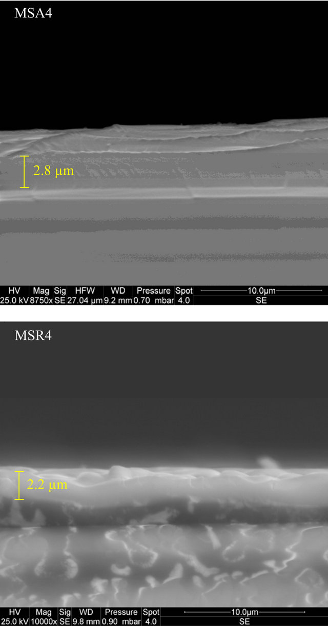
Figure 1. Cross section SEM images of MSA4 and MSR4. Boundaries and average thickness of each layer is reported on each image.
temperature.
3. Results and Discussion
3.1. Cadmium Incorporation
To determine the optical band gap Eg, we have used Tauc et al.’s plot [13] where the absorption coefficient a is a parabolic function of the incident photon energy (E = hn) and optical band gap Eg. This relation is given by:
 (1)
(1)
where A is function of refractive index of the material, reduced mass and speed of light.
The plot of (aE)2 as a function of the energy of incident radiation for the Zn(1−x)CdxO solid solution deposited on a-(MSAi) and r-(MSRi) plane sapphire substrate (i = 1, 2, 3 and 4) has been shown in Figure 2.
The energy band gap is obtained from intercept of the extrapolated linear part of the curve with the energy axis.
As seen in Figure 2, the Zn(1−x)CdxO films shows
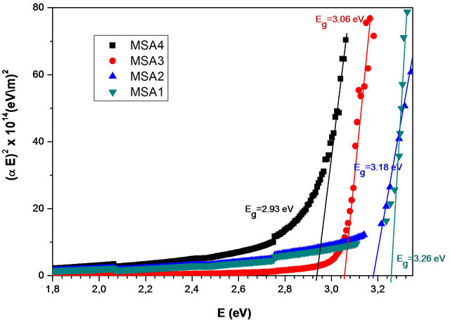
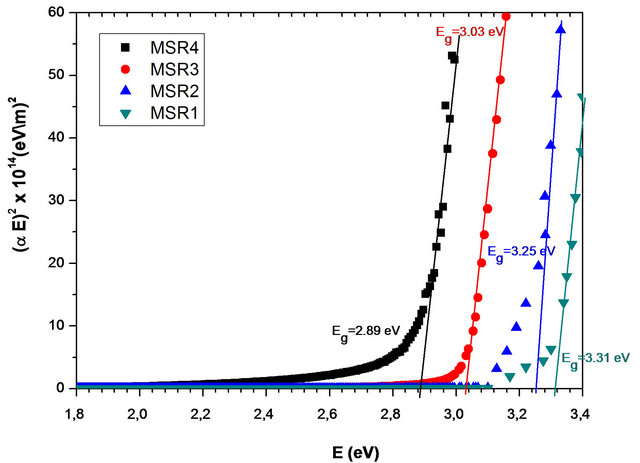
Figure 2. Plots of (aE)2 as a function of photon energy (E) for the Zn(1−x)CdxO solid solution deposited on a-(MSAi) and r-(MSRi) plane sapphire substrate (i = 1, 2, 3 and 4).
shrinkage in energy gap, which provides supportive evidence that Cd incorporates in ZnO. The cadmium concentrations in these layers deposited on aand r-plane sapphire substrate are determined from energy band gap (Eg) equation established by T. Makino et al. [6], where we have used respectively Eg (x = 0) deduced from sample MSA1 and MSR1. The corresponding values of cadmium concentration at % have been given in Table 1. In our previous work [14], the Cd incorporation in Zn(1−x) CdxO has been shown to be nearly twice as high on yield on aand r-plane as the Cd incorporation yield obtained on c-oriented substrate, indicating Cd incorporation is favored in the non polar orientation.
3.2. Structural Properties
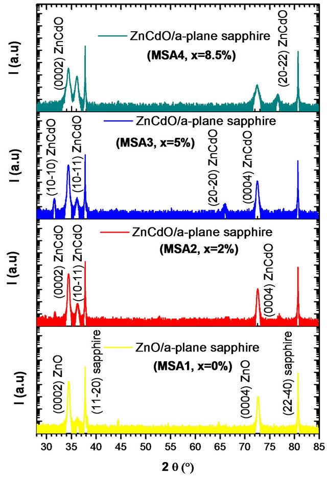
Figure 3 shows the X-ray diffraction (XRD) pattern for ZnCdO grown on aand r-plane sapphire substrate. The 2q - q scan revealed that all the films had wurtzite phase and no indications of any rocksalt phase related to segregate CdO within the layers are detected. The pattern of MSAi (i = 1, 2, 3 and 4) (Figure 3(a)) showed, in addition to substrate peaks  and
and , peaks located at 2q = 31.25˚, 34.32˚, 36.03˚, 72.35˚ and 76.55˚ which are respectively assigned to the peaks
 , (0002),
  , (0004) and
  of layer. The layer peak (000l) intensities are more important than others revealing the presence of a preferred orientation along the direction [0001] that coincides with the orientation of the sapphire substrate. However, in addition to the
  reflection and its harmonic from the r-plane sapphire substrate, only the ZnCdO
  reflection and its harmonic were observed (Figure 3(b)) which confirms the a-plane orientation of the layer [12,15-18].
We also note in Figure 3 (right one), a slight shift of layer peaks to small angles in function of x cadmium composition increase. The mosaicity of the film can be characterized by measuring the corresponding w-rocking curve of the layer peak diffraction, which is shown in Figure 4.
The full widths at half maximum (FWHMs) of the layers peak were reported in Table 2. FWHM increases with Cd composition indicating a degradation of the crystalline quality of the layers. For maximum Cd composition obtained, FWHM is about 1.27˚ for sample MSA4 which is higher compared with 0.90˚ for sample MSR4 although the Cd composition in this sample is more important than that of MSA4.
We have used high resolution X-ray diffraction on symmetric and asymmetric reflections which enables us to precisely measure layer lattice parameters. The lattice parameters of Zn(1−x)CdxO deposited on aand r-plane sapphire substrate are listed in Table 3. The experimental
 (a)
(a)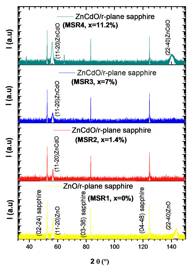 (b)
(b)
Figure 3. 2q - q scan pattern of Zn(1−x)CdxO solid solution deposited on (a) a-(MSAi) and (b) r-(MSRi) plane sapphire substrate (i = 1, 2, 3 and 4).
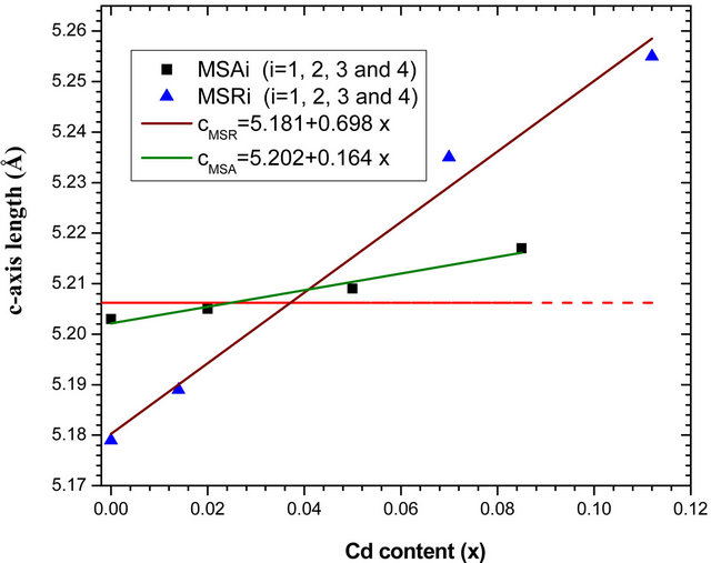
errors of lattice parameter are estimated at 0.003 Å. The a-, c-axis lengths determined by HRXRD, the ratio c/a and the cell volume are plotted as functions of Cd concentration in Figures 5(a)-(d) respectively. Corresponding parameters of bulk ZnO (a0 = 3.2495 Å and c0 = 5.2062 Å) [19] are also represented in dashed line and the solid lines are the linear fit to the corresponding experimental values.
The increase of lattice constant is due to the fact that the covalent radius of Cd2+ (1.48 Å) is larger than that of Zn2+ (1.25 Å) and therefore the substitution of Zn2+ ions by Cd2+ induces a lattice expansion [20,21]. We note a practically linear variation of lattice parameters, c/a ratio and cell volume according to Cd composition. We note that the variation as function of x cadmium content of layer lattice parameter a deposited on a-plane sapphire
Table 2. FWHMs of layer Zn(1−x)CdxO peak deposited on (a) aand (b) r-plane sapphire substrate for each cadmium concentration at % obtained.
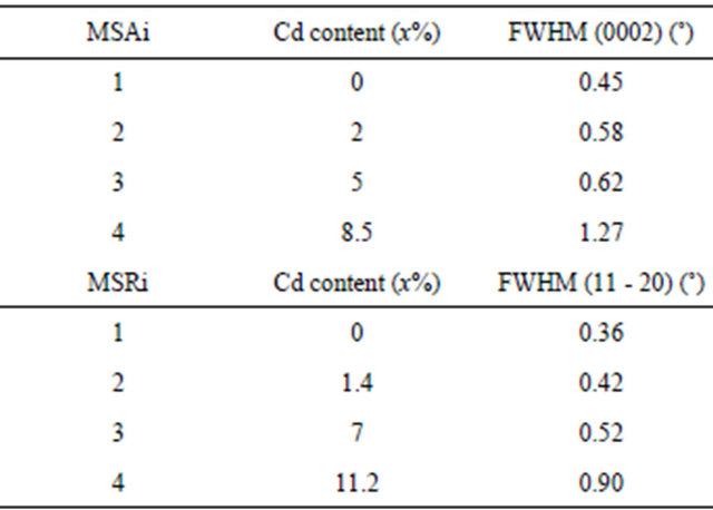
Table 3. Lattice parameters in Zn(1−x)CdxO solid solutions deposited on aand r-plane sapphire, c/a ratio and cell volume as the function of cadmium concentration at %.
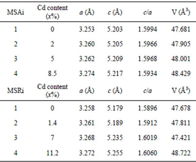
substrate is nearly twice as great as than that deposited on r-plane. On the contrary, we find that the evolution as function of x cadmium content of layer lattice parameter c deposited on r-plane is just over 4 times larger than that deposited on a-plane. This difference is clearly seen in Figure 5(c) where the ratio c/a decreases as function of x for samples MSAi whereas it increase for MSRi. But the increase in cell volume of the two samples series as cadmium x content is close. At high cadmium incorporation, the cell volume varied respectively by 1.7% and 2.33% for MSA4 and MSR4 from that of bulk ZnO. For the layer MSA4, this variation is in good agreement with the value (1.8%) obtained by Zûñiga-Pérez et al. [12] for the same x cadmium incorporation but the solid solution is deposited on r-plane sapphire substrate. In case of MSR4, the percentage variation 2.33% is close to that calculated (2.4%) by the quadratic fit dependence estab-
 (a)
(a)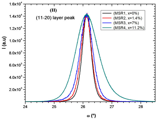 (b)
(b)
Figure 4. w-rocking curve of layer peak diffraction deposited on (a) aand (b) r-plane sapphire substrate for each cadmium concentration at % obtained.
lished in reference [12].
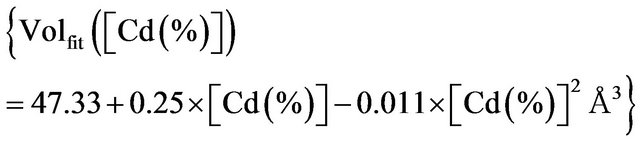
So the maximum attained cell volume variation of 2.33% is achieved before phase separation occurs (xmax = 11.2%), whereas it was of 1.8% for polycrystalline Zn(1−x)CdxO film and respectively 1.7% and 0.9% for c-oriented layer grown on ZnO and c-plane sapphire substrate [22].
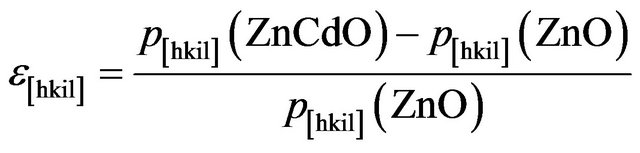
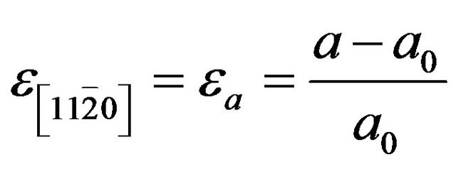
In order to compare the effect of Cd incorporation along [hkil] direction, we define the strain in the Zn(1−x)CdxO layer as:
 (2)
(2)
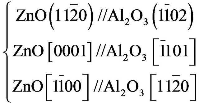
where  is the periodicity along the [hkil] direction of the ZnCdO film and bulk ZnO [18]. Therefore and by considering the epitaxial relationships of ZnO on r-plane [12,18,19,23-27]:
 (a)
(a)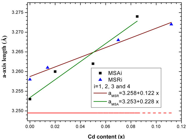 (b)
(b) (c)
(c)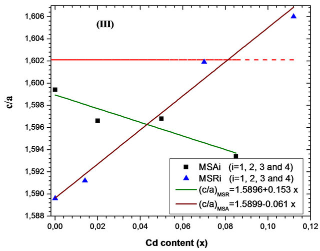 (d)
(d)
Figure 5. Cadmium content x dependence of (a) a-axis lattice length, (b) c-axis lattice length, (c) the ratio c/a and (d) the cell volume. In all cases the dashed line represents the corresponding parameters of bulk ZnO [19]. In all case, the solid lines are the linear fit to the corresponding experimental values.
 (3)
(3)
the deformation out-off the growth plane, i.e. in the direction 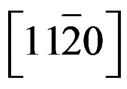 is:
is:
 (4)
(4)
and that in the growth plane are: 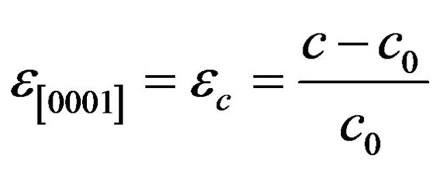 and
and
 (5)
(5)
a0 and c0 are lattice parameters of ZnO completely relaxed (bulk) [19]. Figure 6 shows the strain in MSRi layers as function of x cadmium content. The strain
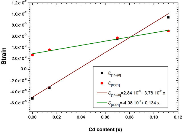
Figure 6. Epitaxial strain  and
and  of ZnCdO/r-plane sapphire as a function of cadmium content x. the solid lines are the linear fit to the corresponding experimental values.
shows a linear dependence on Cd content. The slope of the fitting curves of strain parallel to [0001] is found to be 3.5 times larger than that parallel to , which indicates that the Cd incorporation induces greater lattice deformation along [0001] than
 . In our case, the deformations
  and
and  are identical because we could not quantify any difference between the periodicity along both direction
  and
and , if it exists, for experimental errors.
3.3. Surface Morphology
Figure 7 shows the film morphology of Zn(1−x)CdxO grown on aand r-plane sapphire substrate (scan area 5 µm ´ 5 µm) as function of cadmium content.
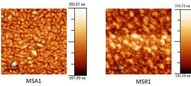
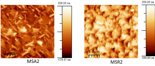
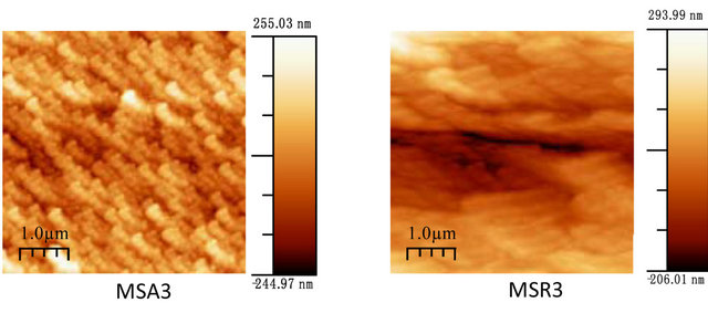
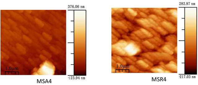
Figure 7. AFM images of Zn(1−x)CdxO deposited on a-(MSAi) and r-plane sapphire (MSRi) (i = ) as function of Cd content.
Upon inspection of the images, the surface morphology of ZnO deposited on a-plane sapphire substrate consists of rounded grains, same one appears slightly elongated and the measured root-square (rms) surface roughness of this film being 40 nm. But for layer MSR1 a two-dimensional growth is obtained with rms surface roughness about 24 nm. For solid solution layers MSA2, we can see in AFM image a hexagonal disk. This morphology shape is also reported by F. Lia et al. [26] and Y. Peng et al. [27] where it seems that the growth of ZnO along the c-axis is blocked.
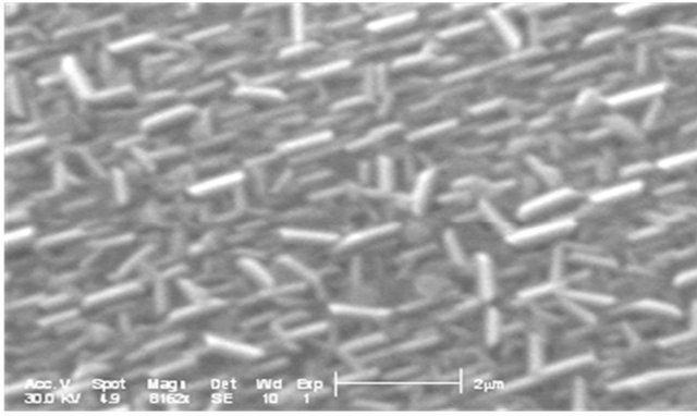
For MSA3 and 4, AFM images show an elongation and coalescence of grain more important as Cd content increases until the nanorod-like shape appearance (Figure 8(a). However, for solid solution layers grown on r-plane sapphire substrate, the grain coalescence leads to a two-dimensional layer (Figure 8(b)).
The rms surface roughness is measured in the same area for all samples and summarized in Table 4. There is a similar order of rms surface roughness as function of Cd content independently of substrate orientation. The lowest rms roughness surface value is obtained for MS(A/R)3. But rms value for sample MSR4 (x = 11.2%) is nearly half that of MSA4 (x = 8.5%).
 (a)
(a)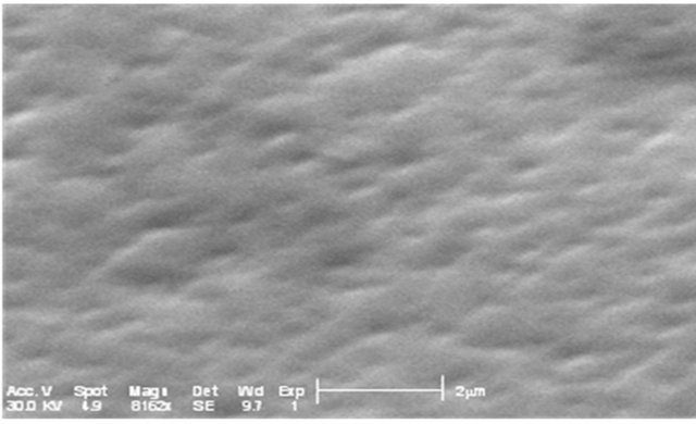 (b)
(b)
Figure 8. Scanning electron microscopy (SEM) images of MSA4 (a) and MSR4 (b) samples.
Table 4. Rms surface roughness of MSAi and MSRi sample (i = ) as function of Cd content.
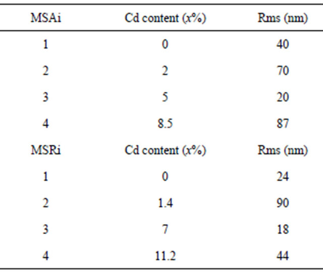
3.4. Photoluminescence Study
As mentioned in the introduction, the incorporation of Cd into the ZnO lattice has been used to tune the emission wavelength of ZnO-based heterostructures into the visible. The bad-gap decrease due to Cd incorporation can be monitored by Pl measurements, although the near bandedge Pl emission energy is lower than the actual bandgap energy due to Stockes’ shift and the exciton binding energy [7].
Pl spectra at room and low temperature of Zn(1−x)CdxO solid solutions grown on aand r-plane sapphire as function of cadmium content are shown respectively in Figures 9(a) and (b). A UV emission can be seen around 3.27 eV of both ZnO layers grown on aand r-plane sapphire [14,24,28,29]. This observed Pl peak of solid solution layer shifts to lower energies and becomes increasingly wide when the cadmium content x increases. In the Pl spectrum of MSA1 at low temperature, there are in addition to the peak of the near band-edge emission at 3.356 eV, a peak around 3.329 eV assigned by Mayer et al. [30], Ozgur et al. [31] and Shirra et al. [32] to defects. As cadmium content x increases, the Pl peak shifts to lower energies and its full width at half maximum (FWHM) increases. At maximum Cd incorporation (x = 8.5%), the position of Pl peaks and the FWHM are respectively 3.15 eV and 320 meV.
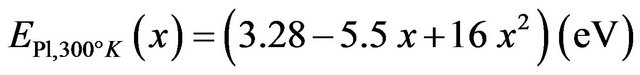
Recently, a structural and optical study was reported by Yamamoto et al. [33] on ternary alloys Zn(1−x)CdxO grown on a-plane sapphire substrates using remoteplasma-enhanced metal-organic chemical vapor deposition. By comparing our results to those calculated by both equations established by these authors with x Cd content obtained for our samples (Table 5), we note that the energies deduced from band-gap energy equation Eg, 300 K(x) are very close to our measurements, proving
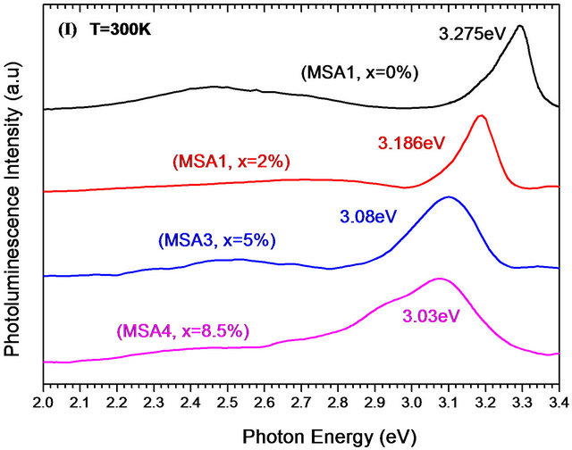
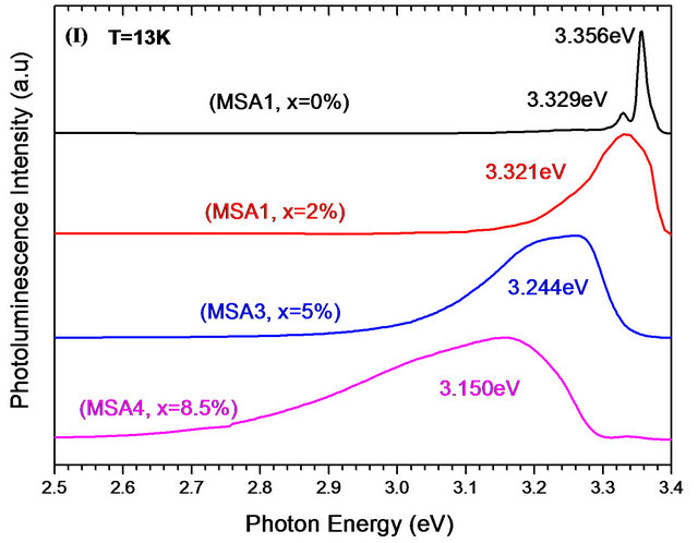
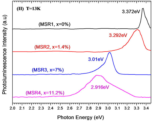
Figure 9. Photoluminescence spectra at room and low temperature of MSAi (a) and MSRi (b) sample (i = ) as function of Cd content.
Table 5. Energy band gap, solid solution Pl peak energy at room and low temperature and those calculated by the equations established by Yamamoto et al. [33] from our cadmium composition.
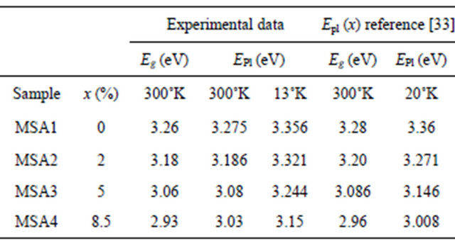
that x cadmium content has been well estimated. But on the contrary, energies deduced from Pl peak energy function EPl, 20˚ K(x) are different from our experimental values.
This is presumably due to cadmium compositional fluctuation and the difference of layers crystalline quality obtained. In fact, low temperature Pl spectroscopy is a suitable method to detect inhomogeneous potential fluctuation because the photo-excited carriers cannot travel a long distance resulting in radiative recombination after relaxation into local potential minima. Same effects of ZnO gap reduction and Pl peak broadening in accordance with the increase of Cd content are observed for solid solution. A maximum energy difference of 456 meV between the pure ZnO sample and MSR4 sample has been found.
By comparing, the room temperature near band-edge Pl peak energies of our samples (MSRi) and that calculated by the equation derived by Zûñiga-Pérez et al. 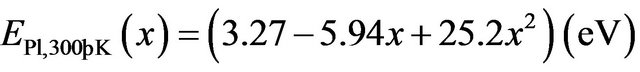 [12], we note that the experimental peak energy position check well the previous expression for x £ 8.5% but a difference of 70 meV is observed for x = 11.2% (Figure 10). By fitting our experimental data, we find the following secondorder polynomial:
Recently, heteroepitaxial growths of Zn(1−x)CdxO film grown on r-plane sapphire substrates by metal-organic chemical vapor deposition is reported by Sartel et al. [34]. In Figure 11, we compare experimental Pl peak energy position at low temperature of our sample MSRi (i = 1 4) with those calculated by the equation established by Yamamoto et al. [33] and Sartel et al. [34]. We can see that the difference between Pl emission energy increases with x Cd content. These few tens meV differrence could be due to local fluctuation in the Cd composition occurring at the atomic scale [35].
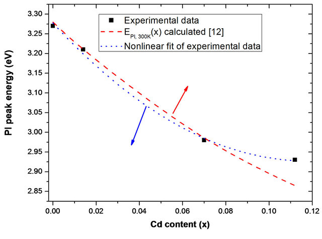
Figure 10. Cd content dependence of room temperature near band edge Pl emission energy of MSRi (i = ) sample. Dashed and dotted line are respectively Pl peak energy calculated by the equation established by Zûñiga-Pérez et al. [12] and the nonlinear fit of the experimental data.
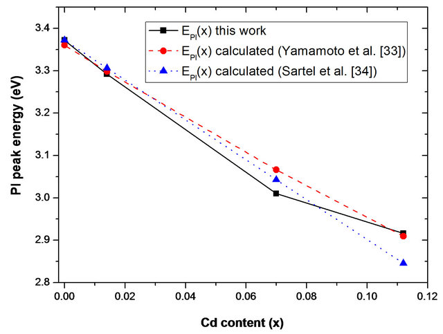
Figure 11. Cd content dependence of low temperature near band edge Pl emission energy of MSRi (i = ) sample. Dashed and dotted line are respectively Pl peak energy calculated by the equation established by Yamamoto et al. [33] and Sartel et al. [34].
3.5. Electrical Properties
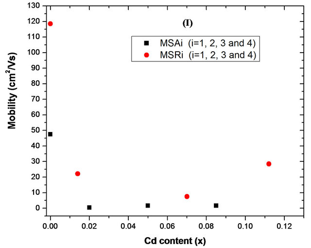
Hall mobility (µ) and carrier concentration (n) of substrates as function of cadmium content x are shown respectively in Figures 12(a) and (b). The type of conducting carriers was confirmed to be n-type for all samples. The film grown on a-plane sapphire has carrier concentration of 4.80 ´ 1018 cm−3 and a mobility of 47.5 cm2/Vs. This mobility value is more important than that reported by Ping et al. [36] (µ = 17.4 cm2/Vs and n = 2.80 ´ 1018 cm−3) but lower than that obtained by K. Iwata et al. [37] (µ = 120 cm2/Vs and n = 7 ´ 1016 cm−3). However, for sample MSR1, carrier concentration and hall mobility are respectively 6.35 ´ 1015 cm−3 and 118.5 cm2/Vs. Although mobility value is smaller than the bulk ZnO value
 (a)
(a)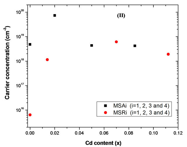 (b)
(b)
Figure 12. Hall mobility and carrier concentration of MSAi and MSRi (i = ) films with different Cd content x measured at room temperature.
of ~200 cm2/Vs [38], it is higher than those of most epitaxial ZnO films grown on c-plane sapphire such as 81 cm2/Vs by Wang et al. [39], 81 cm2/Vs by Polyakov et al. [40] and 103 - 105 cm2/Vs by Jung et al. [41]. But is slightly smaller than those reported by Miyamoto et al. [42] (145 cm2/Vs) and by Chu et al. (highest mobility reached 169.4 cm2/Vs) [43].
An interestingly weak p-type conductivity has recently been observed in non-polar ZnO film grown on r-plane sapphire [36] (hole concentration = 1.33 ´ 1016 cm−3 and mobility = 18.7 cm2/Vs). With cadmium incorporation in ZnO, there is a significant decrease in mobility, which becomes between 0.4 and 0.7 cm2/Vs for solid solution deposited on a-plane sapphire and between 7 and 29 cm2/Vs for those deposited on r-plane sapphire. While the carrier concentration obtained is comparable (1018 - 8 ´ 1018 cm−3) apart from the sample MSA2 where the concentration is 10 times greater. When Cd atoms are incorporated into ZnO, more oxygen vacancies, cadmium interstices and zinc interstices will be produced, which lead to higher carrier concentration [44]. Assuming that scattering mechanisms that govern the electron transport in ZnO and ZnCdO grown on same orientation sapphire substrate are identical, the observed decrease in film mobility can be ascribed to the Cd incorporation. However, the difference observed between the mobility of solid solutions deposited on aand r-plane sapphire is due to the presence and type of structural defects in each case. Microstructure of nonpolar films grown on r-plane sapphire is dominated by the presence of basal stacking faults and related partial dislocation [45]. But for polycrystalline ZnCdO deposited on a-plane sapphire, lattice defects and grain boundary defects increase with Cd incorporation [44].
4. Conclusion
Zn(1−x)CdxO solid solutions have been grown on  (a-plane) and
  (r-plane) sapphire substrate by metal organic chemical vapor deposition in the same condition. The cadmium mole fraction was determined from energy band gap equation established by T. Makino [6]. The maximum Cd content (8.5% and 11.2%) respectively determined for layer deposited on aand r-plane sapphire substrate is significantly larger than thermodynamic solubility limit (2%) [6,46]. Therefore the lattice incorporation sites available in each plane differ and the r-plane could again favor Cd incorporation. The XRD study revealed that all layers exhibit a wurtzite phase. However layer grown on a-plane sapphire substrate are polycrystalline with a preferred [0001] orientation and non-polar, a-plane
  films grown on r-plane sapphire substrate. The microstructure of Zn(1−x)CdxO layer are examined in detail as function of x cadmium content and orientation sapphire substrate employed. The layer lattice is progressively expanded until a volume variation of around 1.8% and 2.33% is obtained respectively for layer deposited on aand r-plane sapphire at a Cd content of 8.5% and 11.2%. As Cd content increases, AFM and SEM images show grain coalescence which lead to nanorod-like shape for layer grown on a-plane sapphire substrate. But two-dimensional growth is observed for solid solution on r-plane sapphire. Pl investigation at room and low temperature of Zn(1−x)CdxO solid solutions grown on aand r-plane sapphire as function of cadmium content are conducted in this work and our results are compared to those of recent bibliography. Near bandedge emission was dominant in Pl spectra which show clearly band gap reduction due to ZnO-CdO alloying. The energy shift between the Pl peaks of ZnO and that of solid solution at highest Cd content for the two orientation sapphire is from 200 to 450 meV. So these Cd concentrations are sufficient for designing Zn(1−x)CdxO/ZnO quantum heterostructures. The decrease of Zn(1−x)CdxO mobility can be ascribed to the Cd incorporation but it is more important in case of films grown on a-plane sapphire. This difference is attributed to the nature of structural defects that appears according to the plane growth orientation.
5. Acknowledgements
The authors would like to thank D. Maaref for proofreading the manuscript.
REFERENCES
- H. Ohta, K. Kawamura, M. Orita and M. Hirano, “Current Injection Emission from a Transparent p-n Junction Composed of p-SrCu2O2/n-ZnO,” Applied Physics Letters, Vol. 77, No. 4, 2000, p. 475-477. doi:10.1063/1.127015
- T. Aoki, Y. Hatawaka and D. C. Look, “ZnO Diode Fabricated by Excimer-Laser Doping,” Applied Physics Letters, Vol. 76, No. 22, 2000, pp. 3257-3258. doi:10.1063/1.126599
- A. Ohtomo, M. Kawasaki, T. Koida, K. Masubuchi and H. Koinuma, “MgxZn1−xO as a II-VI Widegap Semiconductor Alloy,” Applied Physics Letters, Vol. 72, No. 19, 1998, pp. 2466-2468. doi:10.1063/1.121384
- A. Ohtomo, R. Shiroki, I. Ohkubo, H. Koinuma and M. Kawasaki, “Thermal Stability of Supersaturated MgxZn1−xO Alloy Films and MgxZn1−xO/ZnO Heterointerfaces,” Applied Physics Letters, Vol. 75, No. 26, 1999, pp. 4088- 4090. doi:10.1063/1.125545
- T. Makino, C. H. Chia, N. T. Tuan, Y. Segawa, M. Kawasaki, A. Ohtomo, K. Tamura and H. Koinuma, “Radiative and Nonradiative Recombination Processes in LatticeMatched (Cd,Zn)O/(Mg,Zn)O Multiquatum Wells,” Applied Physics Letters, Vol. 77, No. 11, 2000, pp. 1632- 1635. doi:10.1063/1.1308540
- T. Makino, Y. Segawa, M. Kawasaki, A. Ohtomo, R. Shiroki, K. Tamura, T. Yasuda and H. Koinuma, “Band Gap Engineering Based on MgxZn1−xO and CdyZn1−yO Ternary Alloy Films,” Applied Physics Letters, Vol. 78, No. 9, 2001, pp. 1237-1239. doi:10.1063/1.1350632
- A. Nakamura, J. Ishihara, S. Shigemori, K. Yamamoto, T. Aoki, H. Gotoh and J. Temmyo, “Characterization of Wurtzite Zn1−xCdxO Films Using Remote Plasma-Enhanced Metalorganic Chemical Vapor Deposition,” Japanese Journal of Applied Physics, Vol. 43, 2004, pp. L1452-L1454. doi:10.1143/JJAP.43.L1452
- B. Gil, P. Lefebvre, T. Bretagnon, T. Guillet, J. A. Sans, T. Taliercio, and C. Morhain, “Spin-Exchange Interaction in ZnO-Based Quantum Wells, ” Physical Review B, Vol. 74, No. 15, 2006, Article ID: 153302. doi:10.1103/PhysRevB.74.153302
- P. Waltereit, O. Brandt, A. Trampert, H. T. Grahn, J. Menniger, M. Ramsteiner, M. Reiche, and K. H. Ploog, “Nitride Semiconductors Free of Electrostatic Fields for Efficient White Light-Emitting Diodes,” Nature, Vol. 406, 2000, pp. 865-867. doi:10.1038/35022529
- C. R. Gorla, N. W. Emanetoglu, S. Liang, W. E. Mayo, Y. Lu, M. Wraback, and H. Shen, “Structural, Optical, and Surface Acoustic Wave Properties of Epitaxial ZnO Films Grown on
 Sapphire by Metalorganic Chemical Vapor Deposition,” Journal of Applied Physics, Vol. 85, No. 5, 1999, pp. 2595-2602. doi:10.1063/1.369577
 - J. M. Chauveau, M. Laügt, P. Vennegues, M. Teisseire, B. Lo, C. Deparis, C. Morhain, and B. Vinter, “Non-Polar aPlane ZnMgO/ZnO Quantum Wells Grown by Molecular Beam Epitaxy,” Semiconductor Science and Technology, Vol. 23, No. 3, 2008, Article ID: 035005. doi:10.1088/0268-1242/23/3/035005
- J. Zûñiga-Pérez, V. Muñoz-Sanjosé, M. Loreng, G. Benndorf, S. Heitsch, D. Spemann and M. Grundmann, “Facets Evolution and Surface Electrical Properties of Nonpolar m-Plane ZnO Thin Films,” Journal of Applied Physics, Vol. 99, No. 2, 2006, Article ID: 023514. doi:10.1063/1.2163014
- J. Tauc, R. Grigorvici and Y. Yanca, “Optical Properties and Electronic Structure of Amorphous Germanium,” Physica Status Solidi, Vol. 15, No. 2, 1966, pp. 627-637. doi:10.1002/pssb.19660150224
- A. Fouzri, V. Sallet and M. Oumezzine, “A Comparative Structure and Morphology Study of Zn(1−x)CdxO Solid Solution Grown on ZnO and Different Sapphire Orientations,” Journal of Crystal Growth, Vol. 331, No. 1, 2011, pp. 18-24. doi:10.1016/j.jcrysgro.2011.06.056
- S. Liang, H. Sheng, Y. Liu, Z. Huo, Y. Lu and H. Shen, “ZnO Schottky Ultraviolet Photodetectors,” Journal of Crystal Growth, Vol. 225, No. 2-4, 2001, pp. 110-113. doi:10.1016/S0022-0248(01)00830-2
- J. M. Chauveau, P. Vennéguès, M. Laügt, C. Deparis, J. Zûñiga-Pérez, and C. Morhain, “Interface Structure and Anisotropic Strain Relaxation of Nonpolar Wurtzite (11- 20) and (10-10) Orientations: ZnO Epilayers Grown on Sapphire,” Journal of Applied Physics, Vol. 104, No. 7, 2008, Article ID: 073535. doi:10.1063/1.2996248
- G. Saraf, Y. Lu and T. Siegrist, “In-Plane Anisotropic Strain in a-ZnO Films Grown on r-Sapphire Substrates,” Applied Physics Letters, Vol. 93, No. 4, 2008, Article ID: 041903. doi:10.1063/1.2965801
- C. C. Kuo, W.-R. Liu, W. F. Hsieh, C.-H. Hsu, H. C. Hsu and L. C. Chen, “Crystal Symmetry Breaking of Wurtzite to Orthorhombic in Nonpolar a-ZnO Epifilms,” Applied Physics Letters, Vol. 95, No. 1, 2009, Article ID: 011905. doi:10.1063/1.3159470
- F. Vigué, P. Vennéguès, C. Deparis, S. Vézian, M. Laügt and J. P. Faurié, “Growth Modes and Microstructures of ZnO Layers Deposited by Plasma-Assisted MolecularBeam Epitaxy on (0001) Sapphire,” Journal of Applied Physics, Vol. 90, No. 10, 2001, pp. 5115-5119. doi:10.1063/1.1412572
- S.W. Jung, S.J. An, G. Yi, C.U. Jung, S. Lee and S. Cho, “Ferromagnetic Properties of Zn1−xMnxO Epitaxial Thin Films,” Applied Physics Letters, Vol. 80, No. 24, 2002, pp. 4561-4563. doi:10.1063/1.1487927
- C. Liu, F. Yun, B. Xiao, S. J. Cho, Y. T. Moon, H. Morkoc, M. Abouzaid, R. Ruterana, K. M. Yu and W. Walukiewicz, “Structural Analysis of Ferromagnetic MnDoped ZnO Thin Films Deposited by Radio Frequency Magnetron Sputtering,” Journal of Applied Physics, Vol. 97, No. 12, 2005, Article ID: 126107. doi:10.1063/1.1941465
- A. Fouzri, M. A. Boukadhaba, V. Sallet and M. Oumezzine, “Structural Properties and Morphology of Zn(1−x)CdxO Solid Solution Grown on ZnO and c-Plane Sapphire,” Thin Solid Films, Vol. 520, No. 7, 2012, pp. 2582-2588. doi:10.1016/j.tsf.2011.11.027
- J. J. Zhu, T. Aaltonen, V. Venkatachalapathy, A. Galeckas and A. Yu. Kuznetsov, “Structural and Optical Properties of Polar and Non-Polar ZnO Films Grown by MOVPE,” Journal of Crystal Growth, Vol. 310, No. 23, 2008, pp. 5020-5024. doi:10.1016/j.jcrysgro.2008.07.117
- C. R. Gorla, W. E. Mayo, S. Liang and Y. Lu, “Structure and Interface-Controlled Growth Kinetics of ZnAl2O4 Formed at the (110) ZnO/(012) Al2O3 Interface,” Journal of Applied Physics, Vol. 87, No. 8, 2000, pp. 3736-3743. doi:10.1063/1.372454
- S. K. Han, S. K. Hong, J. W. Lee, J. Y. Lee, H.-D. Yun, S.-W. Nam, S.-W. Chang, T. Minegishi and T. Yao, “Structural and Optical Properties of Non-Polar a-Plane ZnO Films Grown on r-Plane Sapphire Substrates by Plasma-Assisted Molecular-Beam Epitaxy,” Journal of Crystal Growth, Vol. 309, No. 2, 2007, pp. 121-127. doi:10.1016/j.jcrysgro.2007.09.025
- F. Li, Y. Ding, P. Gao, X. Xin and Z. L. Wang, “SingleCrystal Hexagonal Disks and Rongs of ZnO: Low-Temperature, Large-Scale Synthesis and Growth Mechanism,” Angewandte Chemie International Edition, Vol. 43, No. 39, 2004, pp. 5238-5242. doi:10.1002/anie.200460783
- Y. Peng, A-W. Xu, B. Deng, M. Antonietti and H. Cötfen, “Polymer-Controlled Crystallization of Zinc Oxide Hexagonal Nanorings and Disks,” The Journal of Physical Chemistry B, Vol. 110, No. 7, 2006, pp. 2988-2993. doi:10.1021/jp056246d
- L. Wang, Y. Yu, W. Fang, J. Dai, Y. Chen, C. Mo and F. Jiang, “High-Quality ZnO Films Grown by Atmospheric Pressure Metal—Organic Chemical Vapor Deposition,” Journal of Crystal Growth, Vol. 283, No. 1-2, 2005, pp. 87-92. doi:10.1016/j.jcrysgro.2005.05.040
- S. W. Jun, W. I. Park, H. D. Cheong, G. C. Yi and H. M. Jang, “Time-Resolved and Time-Integrated Photoluminescence in ZnO Epilayers Grown on Al2O3(0001) by Metalorganic Vapor Phase Epitaxy,” Applied Physics Letters, Vol. 80, No. 11, 2002, pp. 1924-1926. doi:10.1063/1.1461051
- B. K. Meyer, H. Alves, D. M. Hofmann, W. Kriegseis, D. Forster, F. Bertram, J. Christen, A. Hoffmann, M. Strassburg, M. Dworzak, U. Haboeck and A. V. Rodina, “Bound exciton and Donor-Acceptor Pair Recombinations in ZnO,” Physica Status Solidi (B), Vol. 241, No. 2, 2004, pp. 231- 260. doi:10.1002/pssb.200301962
- Ü. Özgür, Ya. I. Alivov, C. Liu, A. Teke, M. A. Reshchikov, S. Doğan, V. Avrutin, S.-J. Cho and H. Morkoç, “A Comprehensive Review of ZnO Materials and Devices,” Journal of Applied Physics, Vol. 98, No. 4, 2005, Article ID: 041301. doi:10.1063/1.1992666
- M. Schirra, R. Schneider, A. Reiser, G. M. Prinz, M. Feneberg, J. Biskupek, U. Kaiser, C. E. Krill, K. Thonke and R. Sauer, “Stacking Fault Related 3.31-eV Luminescence at 130-meV Acceptors in Zinc Oxide,” Physical Review B, Vol. 77, No. 12, 2008, Article ID: 125215. doi:10.1103/PhysRevB.77.125215
- K. Yamamoto, T. Tsuboi, T. Ohashi, T. Tawara, H. Gotoh, A. Nakamura and J. Temmyo, “Strcutural and Optical Properties of Zn(Mg,Cd)O Alloy Films Grown by RemotePlasma-Enhanced MOCVD,” Journal of Crystal Growth, Vol. 312, No. 10, 2010, pp. 1703-1708. doi:10.1016/j.jcrysgro.2010.02.029
- C. Sartel, N. Haneche, C. Vilar, G. Amiri, J.-M. Laroche, F. Jomard, A. Lusson, P. Galtier, V. Sallet, C. Couteau, J. Lin, R. Aad and G. Lérondel, “Growth Studies and Optical Properties of Zn1−xCdxO Films Grown by Metal-Organic Chemical-Vapor Deposition,” Journal of Vacuum Science & Technology A, Vol. 29, No. 3, 2011, Article ID: 03A114. doi:10.1116/1.3567960
- A. Lusson, R. Legros, Y. Marfaing, and H. Mariette, “Alloy-Induced Broadening of Extrinsic and Intrinsic Exciton Luminescence in CdxHg1−xTe,” Solid State Communications, Vol. 67, No. 9, 1988, pp. 851-854. doi:10.1016/0038-1098(88)90116-0
- P. Ding, X. Pan, J. Huang, B. Lu, H. Zhang, W. Chen and Z. Ye, “Growth of p-Type a-Plane ZnO Thin Films on rPlane Sapphire Substrates by Plasma-Assisted Molecular Beam Epitaxy,” Materials Letters, Vol. 71, 2012, pp. 18- 20. doi:10.1016/j.matlet.2011.12.030
- P. Fons, K. Iwata, A. Yamada, K. Matsubara, S. Niki, K. Nakahara, T. Tanabe and H. Takasu, “Nucleation and Growth of ZnO on
 Sapphire Substrates Using Molecular Beam Epitaxy,” Journal of Crystal Growth, Vol. 227-228, 2001, pp. 911-916. doi:10.1016/S0022-0248(01)00927-7
 - D. C. Look, J. W. Hemsky and J. R. Stzelove, “Production and Annealing of Electron Irradiation Damage in ZnO,” Physical Review Letters, Vol. 82, No. 12, 1999, pp. 2552-2555. doi:10.1103/PhysRevLett.82.2552
- S. P. Wang, C. X. Shan, B. Yao, B. H. Li, J. Y. Zhang, D. X. Zhao, D. Z. Shen and X. W. Fan, “Electrical and Optical Properties of ZnO Films Grown by Molecular Beam Epitaxy,” Applied Surface Science, Vol. 255, No. 9, 2009, pp. 4913-4915. doi:10.1016/j.apsusc.2008.12.035
- A. Y. Polyakov, N. B. Smirnov, A. I. Belogorokhov, A. V. Govorkov, E. A. Kozhukhova, A. V. Osinsky, J. Q. Xie, B. Hertog and S. J. Pearton, “Electrical Properties and Deep Traps in ZnO Films Grown by Molecular Beam Epitaxy,” Journal of Vacuum Science & Technology B, Vol. 25, No. 6, 2007, pp. 1794-1798. doi:10.1116/1.2790918
- Y. S. Jung, O. V. Kononenko and W, K. Choi, “Electron Transport in High Quality Undoped ZnO Film Grown by Plasma-Assisted Molecular Beam Epitaxy,” Solid State Communications, Vol. 137, No. 9, 2006, pp. 474-477. doi:10.1016/j.ssc.2005.12.038
- K. Miyamoto, M. Sano, H. Kato and T. Yao, “High-Electron-Mobility ZnO Epilayers Grown by Plasma-Assisted Molecular Beam Epitaxy,” Journal of Crystal Growth, Vol. 265, No. 1-2, 2004, pp. 34-40. doi:10.1016/j.jcrysgro.2004.01.035
- S. Chu, M. Morshed, L. Li, J. Huang and J. Liu, “Smooth Surface, Low Electron Concentration, and High Mobility ZnO Films on c-Plane Sapphire,” Journal of Crystal Growth, Vol. 325, No. 1, 2011, pp. 36-40. doi:10.1016/j.jcrysgro.2011.04.036
- B. J. Zheng, J. S. Lian, L. Zhao and Q. Jiang, “Structural, Optical and Electrical Properties of Zn1−xCdxO Thin Films Prepared by PLD,” Applied Surface Science, Vol. 257, No. 13, 2011, pp. 5657-5662. doi:10.1016/j.apsusc.2011.01.070
- P. Vennegues, J. M. Chauveau, M. Korytov, C. Deparis, J. Zûñiga-Pérez and C. Morhain, “Interfacial Structure and Defect Analysis of Nonpolar ZnO Films Grown on r-Plane Sapphire by Molecular Beam Epitaxy,” Journal of Applied Physics, Vol. 103, No. 8, 2008, Article ID: 083525. doi:10.1063/1.2905220
- H. S. Kang, S. W. Kim, J. H. Kim, S. Y. Lee, Y. Li, J. Sik Lee, J. K. Lee, M. A. Nastasi, S. A. Crooker and Q. X. Jia, “Optical Property and Stokes’ Shift of Zn1−xCdxO Thin Films Depending on Cd Content,” Journal of Applied Physics, Vol. 99, No. 6, 2006, Article ID: 066113. doi:10.1063/1.2186372
NOTES
*Corresponding author.