Circuits and Systems, 2011, 2, 183-189
doi:10.4236/cs.2011.23026 Published Online July 2011 (http://www.SciRP.org/journal/cs)
Copyright © 2011 SciRes. CS
An Ultra Low-Voltage and Low-Power OTA Using
Bulk-Input Technique and Its Application in
Active-RC Filters
Arash Ahmadpour
Department of Electronic Engineering, Lahijan Branch, Islamic Azad University, Lahijan, Iran
E-mail: ar.amp@iau-lahijan.ac.ir
Received March 10, 2011; revised April 29, 2011; accepted May 6, 2011
Abstract
This paper presents the design of a two-stage bulk-input pseudo-differential operational transconductance
amplifier (OTA) and its application in active-RC filters. The OTA was designed in 90 nm CMOS process
and operates at a single supply voltage of 0.5 V. Using a two-path bulk-driven OTA by the combination of
two different amplifiers the DC gain and speed of the OTA is increased. Rail-to-rail input is made possible
using the transistor’s bulk terminal as in input. Also a Miller-Feed-forward (MFF) compensation is utilized
which is improved the gain bandwidth (GBW) and phase margin of the OTA. In addition, a new merged
cross-coupled self-cascode pair is used that can provide higher gain. Also, a novel cost-effective bulk-input
common-mode feedback (CMFB) circuit has been designed. Simplicity and ability of using this new merged
CMFB circuit is superior compared with state-of-the-art CMFBs. The OTA has a 70.2 dB DC gain, a 2.5 MHz
GBW and a 70.8° phase margin for a 20 PF capacitive load whereas consumes only 25 µw. Finally, an 8th
order Butterworth active Biquadrate RC filter has been designed and this OTA was checked by a typical
switched-capacitor (SC) integrator with a 1 MHz clock-frequency.
Keywords: Operational Transconductance Amplifier (OTA), Common-Mode Feedback (CMFB), Bulk-Input,
Switched-Capacitor (SC) Integrator, Miller-Feed-Forward (MFF)
1. Introduction
There are growing strong demands for low-voltage sup-
ply and low-power consumption circuits and systems.
This is especially true for very high integration level and
very large scale integrated (VLSI) mixed-signal chips
and system-on-a-chip. In mixed-signal systems, the ana-
log circuits are combined with digital circuits in order to
get the best performance with low-voltage supply and
low-power consumption. This combination should be in
an optimal way and the optimization process is applica-
tion dependent. Also modern portable applications such
as medical devices and remote wireless sensors require
extending the battery life as well. This trend has forced
designers to develop new approaches more amenable to
low-voltage and low-power integrated circuits and it
poses lots of challenges for all involved such as proc-
esses, devices, circuits, and system architectures [1]. Op-
erational transconductance amplifiers (OTAs) are the key
active building blocks of continuous-time filters. They
can be generally classified into single ended, fully dif-
ferential and pseudo-differential OTAs. Fully differential
OTAs are preferred because they provide larger signal
swing, better distortion performance, better CM noise
and supply noise rejection. The main drawback of using
fully differential OTAs is that a common-mode feedback
(CMFB) circuit must be added. The principle of the CM
control circuit can be easily applied to the design of dif-
ferential structures, and it is well suited for low-voltage
pseudo-differential architectures. This extra circuit is
used to establish the common-mode output voltage and
suppress the common mode signal components [2]. The
speed of the common-mode path should be comparable
to that of the differential path; otherwise the com-
mon-mode noise may be significantly amplified such that
the output signal becomes distorted. Also, the CMFB
circuit is often a source of noise injection and increases
the load capacitance that needs to be driven. Regardless
of the limitations described above, fully differential
OTAs work very well and can substantially im-
184 A. AHMADPOUR
prove the system’s quality, especially in very unfriendly
environments such as mixed-mode applications. How-
ever, at lower supply voltages, pseudo differential OTAs
could be used to avoid the voltage drop across the tail
current source used in the fully differential structures.
Taking the tail current source achieves a larger signal
swing, but it also results in larger CM gain. So it requires
to carefully controlling the CM response for pseudo dif-
ferential OTAs. The reduced supply voltage will cause
many problems when designing analog circuits due to
the reduction in available signal swing. This problem is
magnified due to the fact that the threshold voltage (VT)
of the transistors has been reduced at a slower rate than
the supply voltage. In other words, the threshold-voltage
with decreasing the Power supply never reduces linearly.
If standard analog design techniques continue to be used,
the dynamic range and SNR of the circuits will degrade.
The gain of devices such as amplifiers will also decrease
because cascode transistors can no longer be used since
they limit the output swing. The design of rail-to-rail
input circuits is also made more difficult due to the large
VT which must be overcome. One solution for designing
low-voltage analog circuits is to operate the transistors in
the weak inversion region. The drawbacks to this tech-
nique include a limited input signal swing, an increase in
the mismatch between transistors, a low slew-rate due to
the low bias current levels, and large transistor sizes
[3-6]. In order to avoid these drawbacks a bulk-input
technique can be used, which allows for operation in the
moderate inversion region at supply voltages equal to the
VT of the technology. The voltage applied to the bulk
actually reduces the threshold voltage of the transistor,
which increases the inversion level. One drawback of the
bulk input technique is that the input transistor must sit
in an n-well or p-well, so that its bulk is separate from
the bulk of the rest of the transistors. This is not a prob-
lem in advanced technologies, which make use of triple
well structures. In triple-well processes both the NMOS
and PMOS can have isolated bulk terminals [5]. This
paper presents the design of a novel two-stage bulk-input
pseudo differential OTA, which operates at a supply
voltage of 0.5 V. The circuit was designed using the
90 nm process in digital CMOS technology. Design pro-
cedure for this new merged OTA structure such as main
OTA, CMFB and bias circuits are introduced in Section
2. In Section 3, SC integrator and active RC filter design
are described. Section 4 presents simulation results. Fi-
nally, conclusions and acknowledge are given in Section
5 and 6, respectively.
2. Bulk-Input OTA Circuit Design
2.1. Main Amplifier
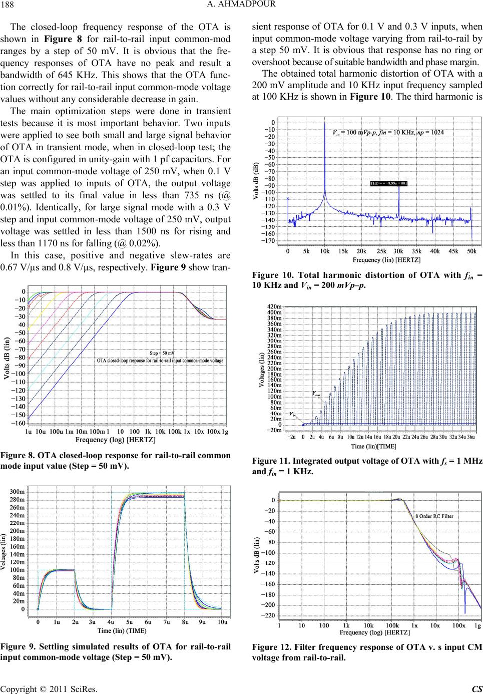
A basic body-input stage, capable of operating with very
low supply voltage is depicted in Figure 1. This struc-
ture is a two-path OTA built by the combination of the
two different amplifiers. In this circuit a PMOS body-
driven OTA is implemented due to the action of M1+,
M1–, M4+ and M4–, and also a current-mirror bulk-input
OTA is composed by transistors M2+, M2–, M3– and M3+.
The OTA input consists of two bulk-input split differen-
tial pairs; some of the ac current generated by the input
transistors is injected to the output transistors, providing
a fast path for the current. The other part of the current is
delivered to the current mirrors of M3+ and M3–. These
are the main transistors which the main portion of the
currents by the factor n transfer to output transistors of
M4+ and M4–. If we suppose M4+ and M4- have equal ef-
fective voltage to M1+ and M1–, their transconductances
are very much greater than bulk- transconductance of
M1+ and M1– (gm4 >> gmb1). It is possible to utilize com-
mon-source amplifier which is parallel and in same
phase with M1 when the input signal is implied to the
gate of M4 via feed-forward (FF) compensate capacitor
Cff (not shown in Figure 1). Moreover, the transistor of
the active load current source operates like a common
source amplifier. This structure increases the gain and
speed of the OTA. M3+ and M3– with diode connections
utilize for M4+ and M4– biasing and use in M2+ and M2–
as a differential loads.
To further improve the differential gain PMOS devices
(M5+, M6+ and M5–, M6–) are added. The body-inputs of
them are a new merged cross-coupled self-cascode pairs
that adds a negative resistance to the output in the form
of g'mb6 and boosts the differential DC gain. The g'mb6 is
the gmb of the self-cascode configuration of M5, M6. Also,
the gate inputs biased at 100 mV, which biases them in
moderate inversion. Moreover, these transistors are a
self-cascode active load for transistors M4+ and M4–
which are common source amplifiers.
Figure 1. One stage of p rop os ed bu lk - inpu t d ifferential pair.
Copyright © 2011 SciRes. CS
A. AHMADPOUR
Copyright © 2011 SciRes. CS
185
2.2. Bulk-Mode Common-Mode Feedback
Circuit and sends a feedback signal Vcm to set the bias voltage at
the gates of input transistors of the OTA. This structure
is able to operate with an ultra low supply voltage (as
low as 0.3 V supply voltage).
The Fully differential OTAs require a common-mode
feedback circuit. A CMFB circuit should behave linearly
and only response to common-mode voltage. Lacking
these features causes increase the THD of the circuit.
Nowadays, designing a CMFB circuit which is able to
operate under an ultra low-voltage supply is very diffi-
cult, mainly because of the difficulty of detecting of CM
voltage. In Reference [5] a CMFB circuit which operated
at 0.5 V by using two resistors to sense the output CM
levels was designed. But this structure increases the die
area and reduces the gain due to longer loads the OTA.
To overcome some of these problems, a CMFB circuit
has been reported [6]. This structure uses of four PMOS
and two NMOS transistors. The NMOS devices is a
bulk-input current mirror, which compares the current of
the PMOS devices and then difference of these current is
fed to the gate of the input transistors for controlling of
the output CM voltages. This paper is given a novel con-
tinuous-time CMFB circuit that is able to operate with an
ultra low-voltage supply. Figure 2 shows the proposed
CMFB circuit for each stage.
In addition, this configuration with minimizing of the
area cost and power consumption is a very cost-effective
CMFB which is much more applicable regarding modern
ultra low-voltage and low-power mixed-signal SoCs.
Simplicity and ability of using this new merged CMFB
circuit to set the output CM voltage of OTA is superior
compared with state-of-the-art CMFB.
To obtain adequate gain, identical gain blocks can be
cascaded so that a two-stage OTA is obtained. Figure 3
show the proposed OTA structure in first and second
stages without bias and CMFB circuits. In order to im-
prove the phase margin and speed of amplifier, we were
used Feed-forward compensation. Finally, the OTA was
stabilized by adding Miller compensation capacitors Cc
with series resistors Rc for right half-plane zero cancela-
tion. The OTA was designed and classified into two
kinds of compensations, such as only Miller compensa-
tion and Miller-Feed-forward (MFF) compensation. The
comparison of two these methods of compensations are
given in Table 1. As can be seen, the MFF compensation
method increases the phase margin and enhances the
open-loop GBW about two times as much.
In this circuit, a combination of two complementary
NMOS and PMOS transistors is used in a bulk-driven
configuration. The output voltage of the CMFB circuit
can be found using the KCL at the output node (Vcm).
The difference between currents of PMOS and NMOS
transistors is fed to the gate of the input transistors of
OTA. The bulks of the PMOS devices Mcp+ (Mcp) con-
nected to the NMOS devices Mcn+ (Mcn) and are utilized
to maintain the output common voltage at the required
level (250 mV), while maximizing the output swing of
the OTA. In other words, the inputs to the CMFB circuit
are the outputs of the OTA, Vo+ and Vo. The CMFB cir-
cuit amplifies the difference between the average of Vo+
and Vo and the desired common level Vcm (250 mV),
Figure 2. Ultra low-voltage bulk-mode CMFB circuit.
Figure 3. Two-stage bulk-input pse udo-diffe rential OTA without bias and CMFB circuits.
A. AHMADPOUR
Copyright © 2011 SciRes. CS
186
Table 1. Comparison of two compensation methods.
Resistors and Capacitors Miller-comp. MFF-comp.
Rc 60 k 68 k
Cc 3 pf 1 pf
Cff - 3 pf
Open-loop GBW 962 KHz 2.5 MHz
Phase-Margin 65° 70.8°
2.3. Reference Current Generator and Bias
Circuit
A low-sensitivity reference current generator and bias
circuit are illustrated in Figure 4. Because the gate and
source of MB3 and MB4 are common for both transistors,
and the aspect ratios are equal, ID MB3 = ID MB4. Also, note
that VGS MB2 = VGS MB1 + RB·ID MB1. Thus,


3
2
3
3
2
2
2
B
B
B
B
B
DM
nox M
DM
BDM
nox M
I
CWL
IRI
CKWL



(1)
In the above mentioned equation, K is the ratio be-
tween the aspect ratios of MB1 and MB2. Rearranging this
expression,

3
2
2
121
.
B
B
DM
nox
BM
ICKWL K
R
 
1
(2)
In the target circuit, k = 1.13 and RB = 1 k, thus ID MB3
= 1.25 uA. As expected, the circuit is independent of the
supply voltage. Transistor MB5 mirrors this current to
generate a stable 2 uA reference current, which is used in
the bias of PMOS devices. In order to ensure that the all
transistors operate in the saturation region, fixed bias
voltages are applied either to the gate of the PMOS and
NMOS transistors in the main OTA and CMFB circuits.
The gate voltage all of the NMOS and PMOS transistors
biased in about Vbn = 350 mV and Vbp = 100 mV, respec-
tively.
3. SC Integrator and Active F ilter Circuit
In order to show that the designed OTA will be useful in
practical analog circuits, this structure was checked by a
typical switched-capacitor (SC) integrator [7,8] with
suitable input frequency 1 KHz and sampling frequency
1 MHz. Figure 5 is shown schematic of this structure. In
switched-capacitor integrator design, we utilized two
clock-frequencies which have no overlap and used Boot-
strapped switches in Reference [9].
Figure 4. Reference current generator and bias circuit.
V
in
V
in+
V
cmi
V
o+
C
L
C
L+
V
i
V
cmi
V
o
V
i+
V
cmo
Figure 5. Fully differential switched-capacitor integrato.
Simulation result of this structure is depicted in Fig-
ure 11.
Filters are systems that can be used to manipulate the
frequency spectrum of signals and they are essential in
many different applications. The low-pass continuous-
time filter is used to limit signal and noise bandwidth and
provide anti-aliasing prior sampling. The analog-to- dig-
ital converter (ADC) digitizes the filtered output to take
the advantages of the Digital Signal Processing (DSP)
unit. The equalizer provides the equalization and the
equalized signal goes to the decoder. The gain/timing
control module is used to adjust the gain of the VGA.
Although we are living in a digital age, many digital
systems interfacing with the real analog world might use
continuous-time filters. There are mainly two types of
filters: digital filters and analog filters. While the data
samples are discrete for digital filters, analog filters
process continuous signals. Analog filters can be further
divided into passive filters and active filters. While pas-
sive filters comprise passive components only such as
resistors, capacitors, and inductors, active filters use ac-
tive devices such as operational amplifiers and/or opera-
tional transconductance amplifiers (OTAs). Active filters
can also be classified into Active-RC, Switched-Ca- pa-
citor (sampled-data filters), OTA-C/Gm-C, and LC fil-
ters. Passive filters do not employ amplifiers and usually
they are off-chip filters and are not suitable for integrated
circuits. But active-RC and SC filters are suitable for low
to medium frequency applications.
A. AHMADPOUR
187
This OTA was tested in an 8th order active Biquadrate
RC filter for maximize the attainable swing. The filter
was built by connecting four 2nd orders Thomas BiQuad
stage to implement the Butterworth function, shown in
Figure 6. The equations of the Two-Thomas biquad fil-
ter as follow:
11
2
22122 1
22
1,,
2
f
ff
s
ffff s
sf
RC R
Q
RRCCC R
RR


A
(3)
where
A
is the gain of integrator and
and Q are
the cut-off frequency and quality factor of integrator,
respectively. Assume Rs2 = Rf2, C
f1 = Cf2, Equation (3)
can be written as:
1
21 21
1,,
2
f
f
f
ff
RR
QA
RC RR


s
(4)
In the above mentioned equation, Q and
A
are de-
termined by the ratio of resistors and both Q and
can be tuned independently [10]. This 8th order Butter-
worth filter consists of four cascaded Thomas biquads;
and the cut-off frequency is about 400 KHz. The filter
was simulated with components values given in Table 2 .
Also, a plot of the frequency response for input CM vol-
tage from rail-to-rail of this filter is shown in Figure 12.
Figure 6. 2nd order Thomas Biquad filter stage.
Table 2. Filter component values.
Components Stage (1) Stage (2) Stage (3) Stage (4)
Rs1 56 k 39 k 47 k 56 k
Rs2 56 k 39 k 47 k 56 k
Rf1 30 k 87 k 87 k 30 k
Rf2 56 k 39 k 47 k 56 k
Cf1 10 pf 10 pf 10 pf 12 pf
Cf2 10 pf 8 pf 5.4 pf 10 pf
4. Simulation Results
To test op-amp’s performance, various configurations
were implemented to simulate application condition.
Based on the analysis procedure described in the previous
sections, an ultra low-voltage OTA at a single 0.5 V sup-
ply voltage was designed. The OTA has been designed in
90 nm CMOS process, and then simulated by Hspice.
Then this structure was checked by a typical SC integra-
tor with a 1 MHz clock frequency. Also a 8th order ac-
tive RC-filter with a 400 KHz cut-off frequency was de-
signed. The simulation results are shown in Figures 7 to
12. Furthermore, Table 3 summarizes the simulated per-
formance of this OTA and comparisons of characteristics
of proposed OTA with state-of-the-art OTAs. The open-lo-
op frequency response of the OTA for the common-mode
input Vcm varying from rail-to-rail by a step 0.01 V was
tested. The amplitudes and the phases of the proposed
OTA were almost independent of the applied Vcm. Figure
5 shows the frequency response of the OTA for Vcm =
0.25 V. The result showed a 70.2 dB DC gain, a 2.5 MHz
bandwidth and a of 70.8° phase margin. For the
closed-loop simulation, the OTA was configured in
unity-gain with 1 pf capacitors.
Figure 7. Open-loop frequency response of OTA for Vcm =
0.25 V.
Table 3. Comparison of characteristics of proposed OTA
with state-of-the-art OTAs.
Ref. [6] Ref. [5] This work Parameters
0.18 µm 0.18 µm
90 nm
Technology
0.5 V 0.5 V
0.5 V
Supply Voltage
65 dB 62 dB 70.2 dB Open-loop DC Gain
550 KHz 10 MHz
2.5 MHz
Open-loop GBW
475 KHz -
645 KHz
Closed-loop GBW
50°
60°
70.8°
Phase-Margin
432
nV/Hz1/2
- 139 nV/Hz1/2
Input ref. noise@1
KHz
19.6 133.3 100 FOM
0.13% 1% 0.119% THD@ 500 mV
20 pf 20 pf
20 pf
Load Capacitors
28 µw 110 µw 25 µw Power Consumption
Copyright © 2011 SciRes. CS
188 A. AHMADPOUR
The closed-loop frequency response of the OTA is
shown in Figure 8 for rail-to-rail input common-mod
ranges by a step of 50 mV. It is obvious that the fre-
quency responses of OTA have no peak and result a
bandwidth of 645 KHz. This shows that the OTA func-
tion correctly for rail-to-rail input common-mode voltage
values without any considerable decrease in gain.
The main optimization steps were done in transient
tests because it is most important behavior. Two inputs
were applied to see both small and large signal behavior
of OTA in transient mode, when in closed-loop test; the
OTA is configured in unity-gain with 1 pf capacitors. For
an input common-mode voltage of 250 mV, when 0.1 V
step was applied to inputs of OTA, the output voltage
was settled to its final value in less than 735 ns (@
0.01%). Identically, for large signal mode with a 0.3 V
step and input common-mode voltage of 250 mV, output
voltage was settled in less than 1500 ns for rising and
less than 1170 ns for falling (@ 0.02%).
In this case, positive and negative slew-rates are
0.67 V/µs and 0.8 V/µs, respectively. Figure 9 show tran-
Figure 8. OTA closed-loop response for rail-to-rail common
mode input value (Step = 50 mV).
Figure 9. Settling simulated results of OTA for rail-to-rail
input common-mode voltage (Step = 50 mV).
sient response of OTA for 0.1 V and 0.3 V inputs, when
input common-mode voltage varying from rail-to-rail by
a step 50 mV. It is obvious that response has no ring or
overshoot because of suitable bandwidth and phase margin.
The obtained total harmonic distortion of OTA with a
200 mV amplitude and 10 KHz input frequency sampled
at 100 KHz is shown in Figure 10. The third harmonic is
Figure 10. Total harmonic distortion of OTA with fin =
10 KHz and Vin = 200 mVpp.
Figure 11. Integrated output voltage o f OTA w ith fs = 1 MHz
and fin = 1 KHz.
Figure 12. Filter frequency response of OTA v. s input CM
voltage from rail-to-rail.
Copyright © 2011 SciRes. CS
A. AHMADPOUR
Copyright © 2011 SciRes. CS
189
about 90 dB below the fundamental. Also, for 400 mV
amplitude, the third harmonic is about 74.4 dB. As can
be seen, the extra harmonics except main harmonic has
been eliminated in this design.
5. Conclusions
In this paper a novel two-stage configuration of the ultra
low-voltage and low-power bulk-input CMOS OTA in
90 nm CMOS process which is able to operate with a
single supply voltage as low as 0.5 V has been presented.
A new merged cross-coupled self-cascode pair was used
and higher DC gain was achieved. In addition, a MFF
compensation was utilized which has been improved the
GBW and phase margin of the OTA. Also, a new bulk-
mode CMFB circuit which no longer loads OTA has been
discussed. A large linear signal swing has been achieved
due to the well controlled CM behavior. Finally this
structure was checked by a typical SC integrator and was
tested in an 8th order active Biquadrate RC filter. Correct
functionality for this configuration is verified from
30˚C to 70˚C. In addition, this structure can be used for
modern ultra low-voltage and low-power mixed- signal
SoCs.
6. Acknowledgements
The work described in this paper is financially supported
by a grant from the Research department of the Islamic
Azad University-Lahijan Branch. Also, the correspond-
ing author wishes to thank Reviewers for their useful
comments and suggestions.
7. References
[1] E. Sanchez-Sinencio and A. G. Andreou, “Low-Voltage
and Low Power Integrated Circuits and Systems,” Low-
Voltage Mixed-Signal Circuits, IEEE Press, New York,
1998.
[2] A. N. Mohieldin, “High Performance Continuous-Time
Filters for Information Transfer Systems,” Ph.D. Disser-
tation, Department of Electrical Engineering, Texas A &
M University, College Station, 2003.
[3] S. Yan and Sanchez-Sinencio, “Low-Voltage Analog
Circuit Design Techniques: A Tutorial,” IEICE Transac-
tions on Analog Integrated Circuits and Systems, Vol.
E00-A, No. 2, 2000, pp. 179-196.
[4] S. S. Rajput and S. S. Jamuar, “Low-Voltage Analog
Circuit Design Techniques,” IEEE Circuit and System
Magazine, Vol. 2, No. 1, 2002, pp. 24-42.
[5] S. Chatterjee, Y. Tsvidis and P. Kinget, “0.5 V Analog
Circuit Techniques and Their Application to OTA and
Filter Design,” IEEE Journal of Solid State Circuits, Vol.
40, No. 12, 2005, pp. 2373-2387.
doi:10.1109/JSSC.2005.856280
[6] M. Trakimas and S. Sonkusale, “A 0.5 V Bulk-Input
OTA with Improved Common-Mode Feedback for Low-
-Frequency Filtering Applications,” Analog Integrated
Circuits and Signal Processing, Springer Press, New
York, 2009, pp. 83-89.
[7] A. Ahmadpour and R. Fouladi, “A Modified High-Perfor-
mance Structure of Low-Voltage CMOS Op-Amp,” Pro-
ceeding of the 2008 IEEE International Conference on
Electron Devices and Solid-State Circuits, Hong Kong,
8-10 December 2008, pp. 1-5.
doi:10.1109/EDSSC.2008.4760687
[8] A. Ahmadpour, “An Ultra Low-Voltage and High-Speed
Amplifier for Switched-Capacitor Applications,” 6th In-
ternational Conference on Electrical Engineering/Elec-
tronics, Computer, Telecommunications and Information
Technology, Vol. 1, Pattaya, 6-9 May 2009, pp. 552-555.
[9] M. Dessouky and A. Kaiser, “Very Low-Voltage Digi-
tal-Audio Modulator with 88-dB Dynamic Range Using
Local Switch Bootstrapping,” IEEE Journal of Sol-
id-State Circuits, Vol. 36, No. 3, March 2001, pp. 349-
355. doi:10.1109/4.910473
[10] R. Schaumann and M. E. Van Valkenburg, “Design of
Analog Filters,” Oxford University Press, Oxford, 2001.