 Circuits and Systems, 2011, 2, 170-182 doi:10.4236/cs.2011.23025 Published Online July 2011 (http://www.SciRP.org/journal/cs) Copyright © 2011 SciRes. CS A Thyristor-Only Input ESD Protection Scheme for CMOS RF ICs* Jin Young Choi, Choongkoo Park Electronic & Electrical Engineering Department, Hongik University, Chungnam, South Korea E-mail: jychoi@hongik.ac.kr Received March 18, 2011; revised April 22, 2011; accepted April 29, 2011 Abstract We propose an input protection scheme composed of thyristor devices only without using a clamp NMOS device in order to minimize the area consumed by a pad structure in CMOS RF ICs. For this purpose, we suggest low-voltage triggering thyristor protection device structures assuming usage of standard CMOS processes, and attempt an in-depth comparison study with a conventional thyristor protection scheme incor- porating a clamp NMOS device. The comparison study mainly focuses on robustness against the HBM ESD in terms of peak voltages applied to gate oxides in an input buffer and lattice heating inside protection de- vices based on DC and mixed-mode transient analyses utilizing a 2-dimensional device simulator. We con- structed an equivalent circuit for the input HBM test environment of the CMOS chip equipped with the input ESD protection devices. And by executing mixed-mode simulations including up to four protection devices and analyzing the results for five different test modes, we attempt a detailed analysis on the problems which can occur in real HBM tests. We figure out strength of the proposed thyristor-only protection scheme, and suggest guidelines relating the design of the protection devices and circuits. Keywords: ESD Protection, HBM, Thyristor, Mixed-Mode Simulation, RF ICs 1. Introduction CMOS chips are vulnerable to electrostatic discharge (ESD) due to thin gate oxides used, and therefore protec- tion devices such as NMOS transistors are required at input pads. A large size for the protection devices is needed to reduce discharge current density and thereby to protect them against thermal-related problems. How- ever, using a large size tends to increase parasitic ca- pacitances added to input nodes generating problems such as gain reduction and poor noise characteristics in RF ICs [1]. To reduce the added parasitics, the protection schemes utilizing thyristor or diode protection devices were sug- gested [2,3] and have been used as fundamental protec- tion schemes in RF ICs. In the protection scheme utiliz- ing thyristor or diode protection devices, it is conven- tional to include a VDD-V SS clamp NMOS device in the input pad structure to provide discharge paths for all possible human-body model (HBM) test modes [4]. A large size for the clamp NMOS device is essential to prevent thermal device failure. Even though the clamp NMOS device does not add parasitics to the input node since it is not connected to it, adopting a large size makes the design to consume an excessive area for the pad structure. This requirement can be a serious limitation in a chip where a pad size is a critical issue in chip design. In this paper, we suggest an input protection scheme utilizing low-voltage triggering thyristor devices only without using a clamp NMOS device in input pad struc- ture. This scheme can be implemented into input pad structures of CMOS RF ICs to provide protection against HBM and MM (Machine mode) discharge events. We present a comparative analysis result of the proposed scheme and the conventional thyristor protection scheme incorporating a clamp NMOS device. The characteristics of the latter scheme are already presented in [4]. A 2-dimensional device simulator, together with a circuit simulator, is utilized as a tool for the comparative analysis. The analysis methodology utilizing a device simulator has been widely adopted with credibility [4-6] since it provides valuable information relating the mecha- nisms leading to device failure, which cannot be obtained by measurements only. *This work was supported by 2010 Hongik University Research Fund. (sponsors) 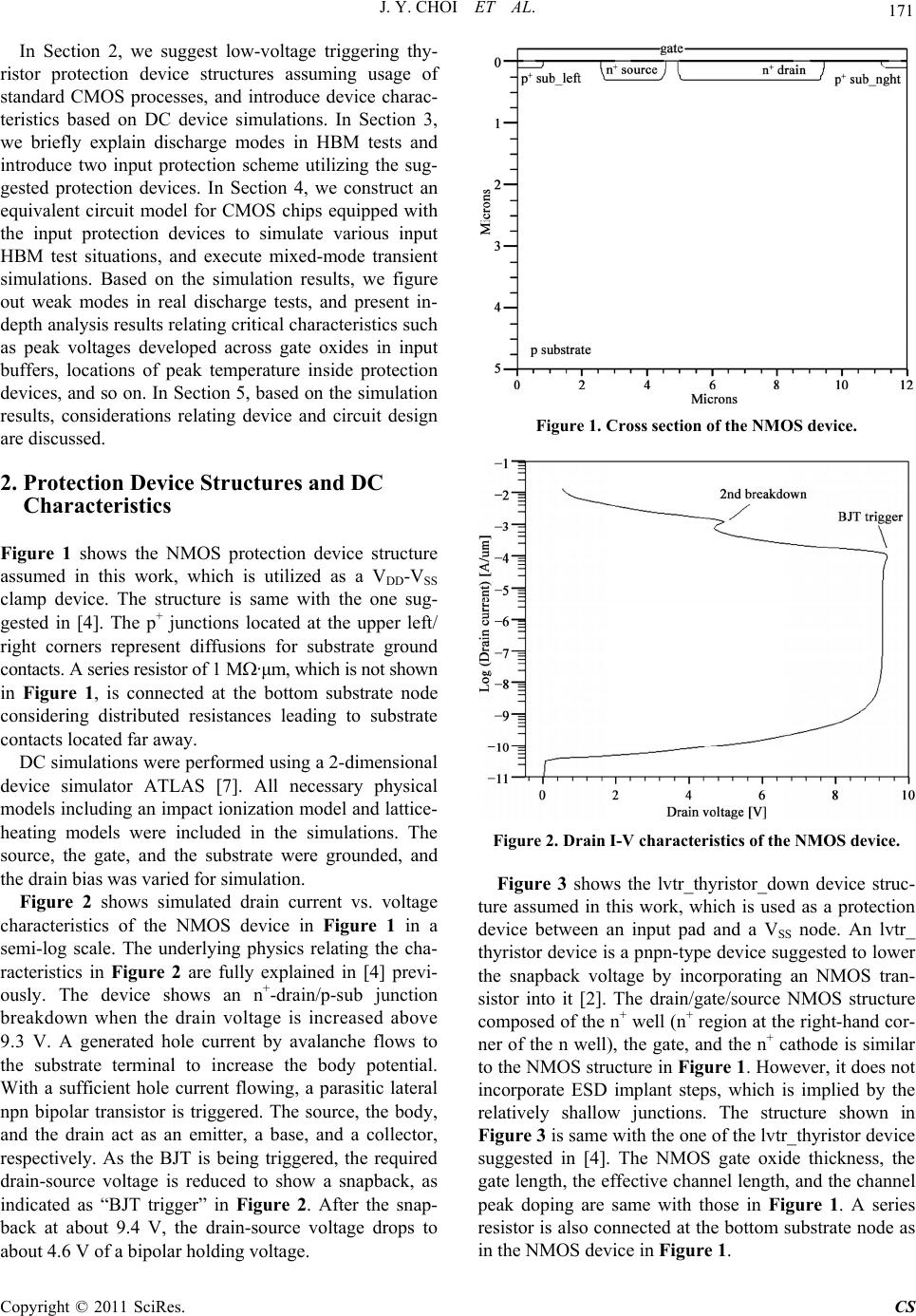 J. Y. CHOI ET AL. 171 In Section 2, we suggest low-voltage triggering thy- ristor protection device structures assuming usage of standard CMOS processes, and introduce device charac- teristics based on DC device simulations. In Section 3, we briefly explain discharge modes in HBM tests and introduce two input protection scheme utilizing the sug- gested protection devices. In Section 4, we construct an equivalent circuit model for CMOS chips equipped with the input protection devices to simulate various input HBM test situations, and execute mixed-mode transient simulations. Based on the simulation results, we figure out weak modes in real discharge tests, and present in- depth analysis results relating critical characteristics such as peak voltages developed across gate oxides in input buffers, locations of peak temperature inside protection devices, and so on. In Section 5, based on the simulation results, considerations relating device and circuit design are discussed. 2. Protection Device Structures and DC Characteristics Figure 1 shows the NMOS protection device structure assumed in this work, which is utilized as a VDD-VSS clamp device. The structure is same with the one sug- gested in [4]. The p+ junctions located at the upper left/ right corners represent diffusions for substrate ground contacts. A series resistor of 1 M·μm, which is not shown in Figure 1, is connected at the bottom substrate node considering distributed resistances leading to substrate contacts located far away. DC simulations were performed using a 2-dimensional device simulator ATLAS [7]. All necessary physical models including an impact ionization model and lattice- heating models were included in the simulations. The source, the gate, and the substrate were grounded, and the drain bias was varied for simulation. Figure 2 shows simulated drain current vs. voltage characteristics of the NMOS device in Figure 1 in a semi-log scale. The underlying physics relating the cha- racteristics in Figure 2 are fully explained in [4] previ- ously. The device shows an n+-drain/p-sub junction breakdown when the drain voltage is increased above 9.3 V. A generated hole current by avalanche flows to the substrate terminal to increase the body potential. With a sufficient hole current flowing, a parasitic lateral npn bipolar transistor is triggered. The source, the body, and the drain act as an emitter, a base, and a collector, respectively. As the BJT is being triggered, the required drain-source voltage is reduced to show a snapback, as indicated as “BJT trigger” in Figure 2. After the snap- back at about 9.4 V, the drain-source voltage drops to about 4.6 V of a bipolar holding voltage. Figure 1. Cross section of the NMOS device. Figure 2. Drain I-V characteristics of the NMOS device. Figure 3 shows the lvtr_thyristor_down device struc- ture assumed in this work, which is used as a protection device between an input pad and a VSS node. An lvtr_ thyristor device is a pnpn-type device suggested to lower the snapback voltage by incorporating an NMOS tran- sistor into it [2]. The drain/gate/source NMOS structure composed of the n+ well (n+ region at the right-hand cor- ner of the n well), the gate, and the n+ cathode is similar to the NMOS structure in Figure 1. However, it does not incorporate ESD implant steps, which is implied by the relatively shallow junctions. The structure shown in Figure 3 is same with the one of the lvtr_thyristor device suggested in [4]. The NMOS gate oxide thickness, the gate length, the effective channel length, and the channel peak doping are same with those in Figure 1. A series resistor is also connected at the bottom substrate node as in the NMOS device in Figure 1. Copyright © 2011 SciRes. CS  172 J. Y. CHOI ET AL. The n+ and p+ anodes in Figure 3 are tied together to serve as an anode. The cathode, the gate, and the sub- strate were grounded, and the anode bias was varied for simulation. Figure 4 shows the simulated DC anode current vs. voltage characteristics of the lvtr_thyristor_down device in Figure 3. The underlying physics relating the charac- teristics in Figure 4 are fully explained in [4] previously. The device shows an n+-drain/p-sub junction breakdown when the anode voltage is increased to above 8.8 V. With a sufficient hole current flowing to the substrate terminal, the p-sub/n+-cathode junction is forward biased triggering a lateral npn bipolar transistor. The n+ well, the p substrate, and the cathode act as a collector, a base, and an emitter, respectively. At this situation, a snapback is monitored as shown in Figure 4. The collector current from the n+ anode flows through the n well to decrease the potential of the region under the p+ anode by an oh- mic drop. When the collector current is large enough, the p+-anode/n-well junction is forward biased to trigger a pnpn (p+-anode/n -well/p-su b/n+-cathode) thyristor, which causes another decrease in the anode voltage, as indi- cated as “pnpn trigger” in Figure 4. The resulting hold- ing voltage drops to about 1 V, which is much smaller compared to 4.6 V of the NMOS device in Figure 2. We note here that the device shown in Figure 3 in- cludes a well conducting thyristor by virtue of the larger n+−p+ anode space. This is verified by the fact that the current level for the pnpn trigger is not much higher than that for the bipolar trigger in Figure 4. As the anode space decreases, the current level for the pnpn trigger increases [8]. If we want to use the lvtr_thyristor_down device in Figure 3 as a protection device between a VDD node and a pad in a thyristor-only protection scheme, we should Figure 3. Cross section of the lvtr_thyristor device. Figure 4. Anode I-V characteristics of the lvtr_thyristor device. connect the p+ anode and the n+ anode to a VDD node, and n+ cathode to a pad, and the common p substrate to a VSS node. In this case, however, we found that a serious problem occurs in a PD mode (a positive ESD voltage applied to a pad with a VDD pin grounded) since there is no forward diode path from the pad to the VDD node. Without the forward diode path provided, an npn (n+-cathode/p-sub/n+-anode) bipolar transistor conducts from the pad to the VDD node to cause a thermal-related problem with a larger holding voltage. Figure 5 shows the lvtr_thyristor_up device, which is suggested in this work to solve the problem. The device apparently in- cludes a forward diode path from the cathode to the an- ode. As we can see in Figure 5, the device needs addition of a p base region, which is provided in most of standard CMOS processes below 0.35 μm to allow forming sim- ple bipolar transistors. Depth of the p-base region was assumed as 0.5 μm, and the base is assumed to have a channel peak doping of 2.35 × 1017 cm–3, which is simi- lar to that of the NMOS structure in the lvtr_thyristor_ down device. Doping profiles of the n well, the n+ and p+ junctions are same with those in the the lvtr_thyris- tor_down device. The NMOS transistor, which is incorporated in the device to lower the snapback voltage, is located inside the p base. The n+ well (n+ region at the left-hand corner of the p base), the gate, and the n+ cathode play the role of the drain, the gate, and the source, respectively. The NMOS structure in the device is very similar to that in the lvtr_thyristor_down device except a small difference in the acceptor doping profile in the body region. We note that, in deep n-well processes, a p well separated from a p substrate can replace the p base. Copyright © 2011 SciRes. CS  J. Y. CHOI ET AL. 173 The n+ and p+ anodes in Figure 5 are tied together to serve as an anode. The n+ and p+ cathodes, the gate, and the substrate were grounded, and the anode bias was va- ried for simulation. Figure 6 shows the simulated DC anode current vs. voltage characteristics of the lvtr_thyristor_up device in Figure 5. The characteristics and the underlying physics are very similar to those of the lvtr_thyristor_down de- vice except that an npn bipolar transistor is formed by the n+-well/p-base/n+-cathode structure and a pnpn thy- ristor is formed by the p+-anode/n-well/p-base/n+-cathode structure. The breakdown voltage in this device corre- sponds to that of the n+-well/p-base junction. Table 1 summarizes the principal DC characteristics of the three protection devices. 3. ESD Protection Schemes Since parasitics added to an input pad should be mini- mized, it is desired to connect fewer number of protec- tion devices to an input pad. An effective way to reduce the number is to use a VDD-VSS clamp device since it provides discharge paths without adding parasitics to an input pad. Figure 7 shows a popular ESD protection scheme utilizing a thyristor device, which minimizes the added parasitics and is chosen for a comparison study with the thyristor-only protection scheme in this work. A CMOS inverter was assumed as an input buffer. The lvtr_thyristor_down device in Figure 3 is used for T1 in Figure 7. The NMOS device in Figure 1 is used for M2. In M2, the drain is connected to VDD, and the gate, the source, and the substrate are connected to VSS. In T1, the p+ and n+ anodes are connected to the pad, and the p substrate and the n+ cathode are connected to VSS. The NMOS gate (G1) in T1 is also connected to VSS to main- tain an off state in normal operations. It is important to locate all the protection devices close to the pad to minimize variation of the gate voltage in the input buffer when an ESD voltage is applied to the pad. Even though same discharge paths can be provided with VDD-VSS clamp devices located in other places, there exists an enhanced danger of oxide failure since the vol- tage applied to the gate oxide of the input buffer may increase due to added high voltage drops in power bus lines with a large discharge current flowing. Figure 8 shows the thyristor-only protection scheme suggested in this work. The lvtr_thyristor_down device in Figure 3 is used for T1, and the lvtr_thyristor_up de- vice in Figure 5 is used for T2. Connection of T1 is same as that in Figure 7. In T2, the p+ and n+ anodes are con- nected to VDD, and the p+ and n+ cathodes are connected to the pad. The NMOS gate (G2) in T2 is connected to the pad to maintain an off state in normal operations. Al- though it is not shown in Figure 8, the p substrate in T2 is connected to VSS. Figure 5. Cross section of the diode device. Figure 6. Anode current-voltage characteristics of the lvtr_ thyristor_up device. Table 1. Principal principal DC characteristics of the pro- tection devices. Protection device Holding Voltage Breakdown voltagee Snapback voltagee NMOS 4.6 V 9.3 V 9.4 V lvtr_thyristor_down 1.0 V 8.8 V 9.4 V lvtr_thyristor_up 1.1 V 9.1 V 9.7 V Copyright © 2011 SciRes. CS  174 J. Y. CHOI ET AL. Figure 7. Protection scheme (1) utilizing a thyristor device. Figure 8. Protection scheme (2) utilizing thyristor devices only. Input protection schemes utilizing thyristor devices only had been suggested [9,10]; however the trigger vol- tages of the suggested devices are too high [9] to be used in recent technologies, or the trigger voltages for the two LVTSCR thyristor devices are uneven [10] due to a dif- ference in hole and electron mobilities resulting uneven trigger voltage for different HBM test modes, which is certainly not beneficial, and the PMOS-triggered thyris- tor structure does not provide a forward diode path from a pad to a VDD node [10] to make the complemen- tary-LVTSCR structure hard to be optimized. While the amount of added capacitance to an input pad is expected to increase to about twice of that in case of using the protection scheme (1), the area consumed by a pad structure is expected to be reduced a lot by eliminat- ing the clamp NMOS device, and the peak voltages ap- plied to gate oxides of input buffers can be reduced somewhat since the series clamp NMOS device disap- pears in a discharge path. Since HBM tests for input pins should include all pos- sible discharge modes, tests are performed for five modes defined as PS, NS, PD, ND, and PTP modes [4]. Main discharge paths for test modes in each protection scheme are shown in Figures 9 and 10. Figure 9 shows main discharge paths for each test mode when using the protection scheme (1). In a PS mode, a pnpn thyristor in T1 provides a main discharge path, and in an NS mode, a forward-biased pn (p+-sub/ n+-anode) diode in T1 provides it. In a PD mode, a pnpn thyristor in T1 and a forward-biased pn (p+-sub/n+-drain) diode in M2 in series provide a main discharge path, and in an ND mode, a parasitic npn bipolar transistor in M2 and a forward-biased pn (p+-sub/n+-anode) diode in T1 in series provides it. In a PTP mode, a pnpn thyristor in T1 and a forward-biased pn (p+-sub/n+-anode) diode in T3, which is located in the other pad, in series provide a main discharge path. Figure 9. Main discharge paths for each test mode in the protection scheme (1). Copyright © 2011 SciRes. CS  J. Y. CHOI ET AL. Copyright © 2011 SciRes. CS 175 Figure 10. Main discharge paths for each test mode in the protection scheme (2). Local lattice heating is proportional to a product of current density and electric field intensity, and therefore temperature-related problems in the protection devices can occur in the parasitic npn bipolar transistor rather than in the forward-biased diode or in the pnpn thyristor since the holding voltage of the bipolar transistor is much larger. Therefore the width of the lvtr_thyristor_down device can be small, however, we should assign a suffi- cient device width to M2 considering an ND mode. Figure 10 shows main discharge paths for each test mode when using the protection scheme (2). In a PS mode, a pnpn thyristor in T1 provides a main discharge path, and in an NS mode, a forward-biased pn (p+-sub/ n+-anode) diode in T1 provides it. In a PD mode, a for- ward-biased pn (p+-cathode/n+-anode) diode in T2 pro- vides a main discharge path, and in an ND mode, a pnpn thyristor in T2 provides it. In a PTP mode, there exist two main discharge paths. One is a series path composed of a forward-biased pn (p+-cathode/n+-anode) diode in T2 and a pnpn thyristor in T4, and the other is a series path composed of a pnpn thyristor in T1 and a forward-biased pn (p+-sub/n+-anode) diode in T3. Since the holding voltages of the thyristor devices are not large, widths of all the thyristor devices don’t need to be large. 4. Mixed-Mode Transient Simulations Figure 11 shows an equivalent circuit of an input HBM test situation assuming a PS mode, which is fully ex- plained in [4] previously. VESD is a HBM test voltage, and a switch S1 charges CESD and then a switch S2 initi- ates discharge. By utilizing time-varying resistors for the switches, the switching times of S1 and S2 were set short as 0.15 ns. In Figure 11, a VDD-VSS clamp NMOS protection de- vice M2 and a protection device T1 form a representative protection circuit in the input pad, assuming usage of the protection scheme (1). In case of using the protection scheme (2), M2 is eliminated, and the additional protec- tion device T2 should be inserted between the VDD node and the pad. A CMOS inverter is assumed as an input buffer inside a chip, which is modeled by a capacitive network. Cngate and Cpgate represent gate-oxide capacitances of an NMOS transistor and a PMOS transistor, respectively. Cds repre- sents an n-well/p-sub junction capacitance. 0.1 pF, 0.1 pF, and 0.01 pF were assumed for Cngate, Cpgate, and Cds, re- spectively. Using ATLAS, we performed mixed-mode transient simulations utilizing the equivalent circuit in Figure 11 equipped with two different input protection circuits shown in Figures 7 and 8. When a mixed-mode simula- tion is performed, the active protection devices are solved by device and circuit simulations simultaneously. For all the mixed-mode transient simulations per- formed for each test mode, VESD = ±2000 V was assumed. To have fair comparison on ESD robustness of the dif- ferent protection schemes, widths of the protection de- vices were adjusted to maintain utmost peak lattice tem- perature inside the protection devices below 500 K in all the mixed-mode simulations, resulting 250 μm, 20 μm, and 20 μm for M2, T1, and T2, respectively.  176 J. Y. CHOI ET AL. As an example of the mixed-mode simulation results, Figure 12 shows variation of the anode current of T1 as a function of time in a PS mode in case of using the pro- tection circuit (1) in Figure 7. The anode current peaks up to 1.37A, and shows decaying characteristics with a time constant of roughly RESDCESD = 0.15 μs, which can be expected from the equivalent circuit in Figure 11. Figure 13 shows variations of the voltages developed across Cngate and Cpgate in the input buffer from the same simulation result. In Figure 13, the pad voltage is not shown since it is almost same with the voltage developed across Cngate. From the DC simulation result in Figure 4, we can es- timate transient discharge characteristics of T1, which lies in the main discharge path in this case. When a posi- tive ESD voltage is applied, the developed voltage across the device will increases at least up to the snapback vol- tage (9.4 V). As the bipolar transistor and the pnpn thy- ristor are triggered in order, the developed voltage will drop down to the holding voltage (1 V) and main dis- charge will proceed. In the later stage of discharge when the discharge current decreases below the holding current for the thyristor action, the developed voltage will in- crease again at most up to the snapback voltage (9.4 V) and will remain constant around the breakdown voltage (8.8 V) for some duration even though the discharge current decreases. As the discharge current decreases further, the device will go out of the breakdown mode and the developed voltage will decrease towards zero to end the discharge. Figure 11. Equivalent circuit of an input-pin HBM test situation. Figure 12. Variation of the anode current of T1 in a PS mode when using the protection circuit (1). Figure 13. Variations of the voltages developed on Cngate and Cpgate in a PS mode when using the protection circuit (1). Copyright © 2011 SciRes. CS  J. Y. CHOI ET AL. 177 With the expectation above in mind, let’s examine the results shown in Figures 12 and 13. From the results shown in Figures 12 and 13, we can see that the parasitic bipolar transistor in T1 is triggered when the pad voltage in the early stage of discharge increases to about 12.8 V at 0.77 ns after S2 in Figure 11 is closed. The trigger voltage is lager than the expected DC value probably due to the time needed for charge redistribution. Main dis- charge through the pnpn thyristor proceeds as the pad voltage, which is equal to the anode-cathode voltage of T1, drops to the holding voltage of about 2 V. The pad voltage decreases down to 1 V as the discharge current decreases with time. We can also see that the pad voltage increases again and reaches to 6.5 V at about 0.9 μs, when the anode current is reduced below the holding current for the pnpn thyristor action, and decreases very slowly thereafter. We confirmed from additional simula- tions that it takes 510 ms for the pad voltage to decrease down to 3 V. We also confirmed that main components of the anode current at 0.9 μs are the leakage current through the n-well/p-sub junction and the weak-inversion MOS current. The developed peak voltage in this later stage of discharge is smaller than the breakdown voltage (8.8 V) of the lvtr_thyristor device shown in Figure 4. This seems to be caused by the long duration (0.9 μs) of the main discharge by virtue of the excellent conducting pnpn thyristor. We confirmed that, with the sufficient discharge through the pnpn thyristor, the remaining dis- charge current level in this stage of discharge is only about 40 nA, which is too low for T1 to conduct in a breakdown mode. We also confirmed from an additional simulation that, if we decrease the n+/p+ anode contact space down to 0.7 μm, the pnpn thyristor turns off earlier at 0.815 μs and the developed peak voltage increases up to 9 V with the remaining discharge current level of about 0.1 mA, which is certainly high enough for the device to conduct in a breakdown mode. Figure 13 shows that, in overall, a lower voltage by about 1 V is developed on Cpgate since the VDD node does not lie in the main discharge path. Figure 14 shows variations of the voltages developed on Cngate and Cpgate in a PS mode in case of using the pro- tection circuit (2) in Figure 8. We confirmed that the variation of the anode current of T1 is similar to that in Figure 12. As we can see from Figure 14, the variation of the pad voltage, which is again almost same with the voltage developed on Cngate, is similar to that in case of using the protection circuits (1). The parasitic bipolar transistor in T1 is triggered when the pad voltage in the early stage of discharge increases to about 12.8 V at 0.77 ns after S2 is closed. Main discharge through the pnpn thyristor pro- ceeds as the pad voltage drops to the holding voltage of about 2 V. Figure 14. Variations of the voltages developed on Cngate and Cpgate in a PS mode when using the protection circuit (2). The pad voltage increases again and reaches to 6.2 V at about 0.9 μs, and decreases very slowly thereafter. We confirmed that the pad voltage (6.2 V) in this case is slightly lower than that in case of using the protection circuit (1) due to a difference in the current components. We confirmed that, when the pad voltage increases to 6.2 V, a pnp (p+-cathode/n-well/p+-sub) bipolar transistor in T2 is triggered and the pad voltage is limited by the pnp bipolar holding voltage. Since the holding voltage is somewhat large, thermal heating may cause a problem. However, we confirmed that the bipolar current level at this moment is too low to cause thermal heating. The components of the anode current in T1 in this later stage of discharge also include the leakage current through the n-well/p-sub junction and the weak-inversion MOS cur- rent, however the bipolar current through T2 is a major discharge current for some duration. Due to this current component, the pad voltage in this later stage of dis- charge decreases faster, compared to the case using the protection circuit (1). We confirmed that it takes 23 ms for the pad voltage to decrease down to 3 V. In Figure 14, we can see that the voltage developed across Cpgate remains low all the time. This is because the p+-cathode/n+-anode diode is conducting if the VDD-pad voltage becomes larger than the forward diode drop. In the later stage, there is almost no conduction through T2, and the voltage stays close to zero. 4.1. Voltages across the Gate Oxides in the Early Stage of Discharge For the two PS modes analyzed above, the trigger time for T1 is 0.77 ns. Due to this trigger time, the voltage Copyright © 2011 SciRes. CS  178 J. Y. CHOI ET AL. (12.8 V) larger than the DC snapback voltage is devel- oped across T1 right after S2 is closed, resulting the high voltage developed on Cngate in the early stage of dis- charge in Figures 13 and 14. Depending on test modes, larger peak voltages across the gate oxides in the input buffer appear at Cngate or Cpgate. If we define the test modes, which produce larger peak voltages in the mixed-mode transient simulations performed for 5 test modes, as weak modes, the results can be summarized as shown in Table 2. In Table 2, 13.3 V on Cpgate in the PD mode in case of using the protection scheme (1) corresponds to a sum of the voltages applied on the pnpn structure in T1 and the forward diode in M2, which can be easily expected from Figures 7 and 9. The voltage applied on the pnpn struc- ture peaks up to 12 V in this case. 13.5 V on Cpgate in the ND mode in case of using the protection scheme (1) cor- responds to a sum of the voltages applied on the npn structure in M2 and the forward diode in T1. The voltage applied on the npn structure peaks up to 10.8 V. 12.3 V on Cpgate in the ND mode in case of using the protection scheme (2) corresponds to the voltage applied on the pnpn structure in T2, which can be easily expected from Figures 8 and 10. The peak voltages in Table 2 can be regarded as ex- cessive; however, durations of the peak voltages applied are very short. We confirmed that, for example, the dura- tions for which the voltages exceed 10 V are at most 0.2 ns. Therefore it may be inferred that the gate oxides in the input buffer won’t be damaged in the early stage of discharge [11]. Notice that the peak voltages can be suppressed by reducing the bipolar trigger voltage of the NMOS tran- sistor in the NMOS protection device or the thyristor protection devices. To make the bipolar trigger voltage of the NMOS transistor even lower than the off-state DC breakdown voltage, the gate-coupled NMOS (gcNMOS) structure [12] can be adopted. It is possible to obtain a similar result by simply in- serting a series resistor between the gate (G2) and VSS nodes of M2 in Figure 7 since the gate-drain overlap capacitance (Cgd) already exists in the NMOS structure [4]. For the lvtr_thyristor_down device, the same tech- nique can be applied since it includes the same NMOS structure in it [4]. For the lvtr_thyristor_up device, the same technique can be also applied. A series resistor inserted between the gate (G2) and the input node in Figure 8 will do the role. We performed addition simulations to confirm that the early peaking can be suppressed by adding the series resistor to the gate node. The results are summarized in Table 3. For the 250 μm M2, a 10 kΩ resistor was in- serted between the gate and VSS nodes. For the 20 μm T1, a 125 kΩ resistor was inserted between the gate and VSS nodes. For the 20 μm T2, a 125 kΩ resistor was inserted between the gate and the input pad nodes. It is certain that the early peaking can be suppressed if needed. 4.2. Voltages across the Gate Oxides in the Later Stage of Discharge Depending on test modes, larger peak voltages across the gate oxides also appears at Cngate or Cpgate in the later stage of discharge. If we define the test modes, which produce larger peak voltages, as weak modes, the results can be summarized as shown in Table 4. We confirmed that use of the gate-coupling techniques does not affect the peak voltages in the later stage of discharge at all. Table 2. Peak voltages developed across the gate oxides in the early stage of discharge. Peak voltage [V] Protection schemeWeak mode Cngate C pgate Time [ns] (1) PS 12.8 0.77 PD 13.3 0.66 ND 13.5 0.82 (2) PS 12.8 0.77 ND 12.3 0.80 Table 3. Peak voltages developed across the gate oxides in the early stage of discharge when adopting the gate-cou- pling technique. Peak voltage [V] Protection schemeWeak mode Cngate C pgate Time [ns] (1) PS 8.7 0.65 PD 9.7 0.57 ND 10.4 0.79 (2) PS 8.7 0.65 ND 8.8 0.69 Table 4. Peak voltage developed across the gate oxides in the later stage of discharge. Peak voltage [V] Protection schemeWeak mode Cngate C pgate Time [μs] (1) PD 7.6 0.92 ND 10.7 0.50 (2) PS 6.2 0.92 ND 8.8 0.89 PTP 7.4 7.9 0.89 Copyright © 2011 SciRes. CS  J. Y. CHOI ET AL. 179 From Table 4, we can see that, in case of using the protection scheme (1), the ND mode is the weakest one. 10.7V developed on Cpgate corresponds to a sum of the breakdown voltage of M2 (9.6 V) and the forward diode drop in T1 (1.1 V) right after the main discharge through M2 and T1 is finished, which can be easily expected from Figures 9 and 7. Differently from the results of the thy- ristor devices in Figures 13 and 14, the peak voltage developed across M2 in this case is about same with the DC breakdown voltage (9.3 V). This is because the bi- polar transistor in M2 is not as excellent conducting as the pnpn thyristor, and the main discharge through the bipolar transistor ends earlier (at 0.5 μs) compared to that through the pnpn thyristor as shown in Table 4. In case of using the protection scheme (2), the ND mode is also the weakest one. 8.8 V developed on Cpgate corresponds to the voltage developed across T2, which is somewhat smaller than the DC breakdown voltage (9.1 V) of T2. In a PTP mode, 7.4 V and 7.9 V are developed on Cngate and Cpgate, respectively, which correspond to the voltages developed across T1 and T4 in Figure 10. We note that high voltages in the later stage of dis- charge can damage gate oxides in input buffers since they last for long time. When judging from the peak vol- tages developed across the gate oxides in the later stage of discharge in Table 4, the weakest modes in case of using the protection scheme (1) is an ND mode, and the PMOS gate oxide is more vulnerable to HBM ESD damages if the gate-oxide thicknesses of the NMOS and the PMOS are same. In case of using the protection scheme (2), the weakest mode is also an ND mode and the PMOS gate oxide is also more vulnerable. When judging from the peak voltages developed, the advantage of the protection scheme (2) over the protec- tion scheme (1) is expected to stand out more as the gate oxide thickness shrinks with advanced process technol- ogy used. 4.3. Location of Peak Temperature and Weak Modes In case of using the protection scheme (1), the utmost peak temperature in a PS mode appears at T1, and Figure 15 shows the variation of peak temperature inside T1. Peak temperature increases up to 473 K at about 0.9 ns just before the pnpn thryristor trigger, but decreases down to 330 K as soon as the pnpn thryristor is triggered since the holding voltage decreases. It peaks again up to 421 K at about 45 ns with increasing discharge current, and decreases slowly with the discharge current decreasing. By examining 2-dimensional temperature distributions, we confirmed that peak temperature at 0.9 ns appears at the n+ well junction, where the electric field intensity is highest, and that at 45 ns appears at the n+ cathode junc- tion, where the current density is highest. If we define the test modes, which produce larger tem- perature increase inside any protection device, as weak modes, the results can be summarized as shown in Table 5. In case of using the protection scheme (1) incorporate- ing the 250 μm NMOS device and 20 μm lvtr_thyris- tor_down device, the weakest mode is the ND mode, and peak temperature appears in M2, which conducts as an npn bipolar transistor. Peak temperature inside M2 ap- pears at the gate-side n+ drain junction. This is the reason for assigning a large spacing between the gate and the drain contact in Figure 1 to avoid drain contact melting. The second weakest mode is the PS mode, and the 1st peak temperature appears in T1, which happens just be- fore the pnpn thyristor is triggered. At this point, peak temperature inside T1 appears at the n+ well junction Figure 15. Peak temperature variation inside T1 in a PS mode when using the protection scheme (1). Table 5. Peak temperature locations and times. Peak temperature Protection scheme Weak mode Peak temp.[°K] Location Time [ns] (1) PS 473 n+ well junction in T1 0.9 421 n+ cathode junction in T1 45 ND495 gate-side drain junction in M233 (2) PS 471 n+ well junction in T1 0.8 421 n+ cathode junction in T1 52 ND471 n+ well junction in T2 0.9 473 n+ cathode junction in T2 44 Copyright © 2011 SciRes. CS  180 J. Y. CHOI ET AL. at the right-hand corner of the n well. However, a prob- lem with contact melting will not occur in this junction since there is no contact on it. The 2nd peak temperature in T1 appears at the n+ cathode junction when it conducts as a pnpn thyristor. Junction engineering such as in- creasing the junction area or adopting ESD ion implanta- tion may be required to restrain temperature increase. However, it will not add parasitics to the input pad since the junction is not connected to it. In case of using the protection scheme (2) incorporat- ing the 20 μm lvtr_thyristor devices, the weakest mode is the ND mode, and the 1st peak temperature appears in T2, which happens just before the pnpn thyristor is triggered. Peak temperature inside T2 appears at the n+ well junc- tion at the left-hand corner of the p base. However, a problem with contact melting will not occur in this junc- tion since there is no contact on it. The 2nd peak tem- perature in T2 appears at the n+ cathode junction when it conducts as a pnpn thyristor. Junction engineering such as increasing the junction area or adopting ESD ion im- plantation may be required to restrain temperature in- crease. This will not add parasitics to the input pad as long as the p-base region is not widened since the n+ ca- thode is located inside the p base. As shown in Table 5, lattice heating characteristics in a PS mode are very sim- ilar to those in case of using the protection scheme (1). We confirmed from additional simulations incorpo- rating the gate-coupling technique that all the tempera- ture peaking prior to 1ns in Table 5 are suppressed be- low 380 K by virtue of the reduced bipolar trigger volt- ages. This can be easily expected from the results shown in Table 3. From the result shown in Table 5, we can see that the 20 μm lvtr_thyristor devices are superior to the 250 μm NMOS device in ESD robustness in terms of thermal heating. Therefore we can save a lot of area consumed by a pad structure by eliminating the large clamp NMOS device. 5. Discussions 5.1. Considerations in Designing the Lvtr_Thyristor_Down Device By performing additional simulations, we figured out that a serious problem could occur if the p-type substrate contacts are not located close to the lvtr_thyristor_down device as shown in Figure 3. When the p+-sub/n +-anode forward diodes in T1 and T3 in Figure 10 turn on in the early stage of discharge in the NS and PTP modes, re- spectively, the parasitic npn (n+-cath-ode/p-sub /n+-anode) bipolar transistor inside this small-sized device can be triggered to increase temperature around the n+ cathode junction a lot, where electric field intensity is high. Therefore it is very important to locate the p+-sub con- tacts close as shown in Figure 3. 5.2. Considerations in Designing the Lvtr_Thyristor_Up Device By performing additional simulations, we also figured out that a similar problem could occur if the n+ anode2 contact at the right-hand side of the p base is not located in the lvtr_thyristor_up device as shown in Figure 5. When the p+-cathode/n+-anode forward diode in T2 in Figure 10 gets on in the early stage of discharge in PD and PTP modes, a parasitic npn (n+-cathode/p-base/ n+-anode) bipolar transistor inside this small-sized device can be triggered to increase temperature around the n+ cathode junction a lot. This can be completely solved by providing an additional p+-cathode/n+-anode2 forward diode path with the n+ anode2 contact as shown in Fig- ure 5. We also figured out that there is an important consid- eration to take care in connecting the gate node (G2) in T2 in Figure 8. Even though G2 can be connected to the VSS node without increasing an off-state leakage in nor- mal operations, this may cause a problem by making the pnpn thyristor in T1 never triggered in the PTP mode shown in Figure 10. This is because the voltage devel- oped between the pad (connected to the n+/p+ cathodes of T2) and the VSS node is restrained below 9 V, which is much smaller than the pnpn trigger voltage of 12.8 V, as a result of capacitive coupling between G2 (connected to the VSS node) and the n+/p+ cathodes of T2. As a result, the discharge current flows mainly through the upper discharge path (Path 1) consisting of T2 and T4 in Figure 10. At the same time, the pnp (p+-cathode/n-well/p+-sub) bipolar transistor in T2 is triggered to provide another discharge path by way of the forward biased pn (p+-cathode/n+-anode) diode in T3. This causes a thermal heating problem by increasing lattice temperature near the p+ sub junction at the right-hand corner of T2 a lot. This pnp (p+-cathode/n-well/p +-sub) bipolar transistor is easily triggered since the p+-cathode/n-well diode is al- ready forward biased due to the conduction through Path 1 in Figure 10. This problem is completely solved by making the pnpn thyristor in T1 easy to be triggered by connecting G2 to the input pad as shown in Figure 8. 5.3. Providing Discharge Paths for VDD-VSS HBM Discharge We have to check that a chip adopting the thyristor-only protection scheme can provide safe discharge paths when VDD-VSS HBM tests are performed. We note that large Copyright © 2011 SciRes. CS  J. Y. CHOI ET AL. 181 clamp devices such as the NMOS device shown in Fig- ure 1 should be located between VDD and VSS buses in VDD and VSS pad structures and also anywhere a space is available to provide discharge paths for VDD-VSS ESD events and also to reduce a VDD bounce during normal operation by increasing the capacitance between the two buses. We note that the bipolar trigger voltage of the clamp NMOS device without the gate-coupling tech- nique was confirmed as less than 11 V relating the result shown in Table 3. Using a single lvtr_thyristor protection device formed by assuming the lvtr_thyristor_down device in Figure 3 (T1) and the lvtr_thyristor_up device in Figure 5 (T2) located side by side on a same substrate, we confirmed by a mixed-mode simulation that the VDD-VSS peak vol- tage of the protection scheme (2) in a VDD-VSS HBM test is 17.6 V. The VDD-VSS voltage decreases down to 4 V (2 V each across T1 and T2) with both of the pnpn thy- ristors in T1 and T2 being triggered. Therefore, in a VDD-VSS HBM ESD test, it is certain that the clamp NMOS devices will provide discharge paths before the pnpn path through T1 and T2 in any of input pad struc- tures is triggered. Also when a surge voltage appears between VDD and VSS buses, the clamp NMOS device will constrain the rail voltage below 11 V to suppress the possibility of latch-up through T1 and T2. Also the latchup cannot per- sist since the conduction through T1 and T2 in series can be maintained only if the VDD-VSS voltage is higher than 4 V, which is higher than the normal supply voltage in recent technologies. 6. Summary We proposed an input protection scheme composed of thyristor devices only to minimize the size of an input pad structure. For this purpose, we suggested the low- voltage triggering thyristor protection device structures assuming usage of standard CMOS processes, and at- tempted an in-depth comparison study with a conven- tional thyristor protection scheme incorporating a clamp NMOS device based on DC and mixed-mode transient analyses utilizing a 2-dimensional device simulator. We analyzed in detail the problems which can occur in real HBM tests to provide useful findings regarding the proposed protection scheme as follows. 1) We figured out weak modes in terms of peak volt- ages developed across gate oxides in input buffers. 2) We figured out weak modes in terms of temperature increase inside the protection devices, and also figured out locations of peak temperature inside the protection devices. 3) We suggested design guidelines for each protection device to minimize temperature increase inside it and to minimize voltages developed across gate oxides in input buffers. 4) We showed how we can incorporate the gate cou- pling technique into the suggested protection devices. 5) We showed that the suggested thyristor-only pro- tection scheme can be made free from CMOS latch-up. 7. References [1] P. Leroux and M. Steyaert, “High-Performance 5.2 GHz LNA with on-Chip Inductor to Provide ESD Protection,” Electronics Letters, Vol. 37, No. 7, 2001, pp. 467-469. doi:10.1049/el:20010271 [2] A. Chatterjee and T. Polgreen, “A Low-Voltage Trigger- ing SCR for on-Chip ESD Protection at Output and Input Pads,” IEEE Electron Devices Letters, Vol. 12, No. 1, 1991, pp. 21-22. doi:10.1109/55.75685 [3] E. R. Worley, R. Gupta, B. Jones, R. Kjar, C. Nguyen and M. Tennyson, “Sub-micron Chip ESD Protection Sche- mes Which Avoid Avalanching Junctions,” Electrical Overstress/Electrostatic Discharge Symposium Proceed- ings, Phoenix, 12 September 1995, pp. 13-20. [4] J. Y. Choi, “A Comparison Study of Input ESD Protec- tion Schemes Utilizing NMOS, Thyristor, and Diode De- vices,” Communications and Network, Vol. 2, No. 1, 2010, pp. 11-25. doi:10.4236/cn.2010.21002 [5] H. Feng, G. Chen, R. Zhan, Q. Wu, X. Guan, H. Xie and A. Z. H. Wang, “A Mixed-Mode ESD Protection Circuit Simulation-Design Methodology,” IEEE Journal of Soi- lid-State Circuits, Vol. 38, No. 6, June 2003, pp. 995- 1006. doi:10.1109/JSSC.2003.811978 [6] B. Fankhauser and B. Deutschmann, “Using Device Si- mulations to Optimize ESD Protection Circuits,” Interna- tional Symposium on Electromagnetic Compatibility , Santa Clara, 9-13 August 2004, pp. 963-968. [7] Silvaco International, “ATLAS II Framework,” Version 5.10.2.R, Silvaco International, Austin, 2005. [8] J.-Y. Choi, W. S. Yang, D. Kim and Y. Kim, “Thyristor Input-Protection Device Suitable for CMOS RF ICs,” Analog Integrated Circuits and Signal Processing, Vol. 43, No. 1, April 2005, pp. 5-14. doi:10.1007/s10470-005-6566-y [9] H. Feng, K. Gong and A. Wang, “A Comparison Study of ESD Protection for RFIC’s: Performance vs. Parasitic,” 2000 IEEE Radio Frequency Integrated Circuits Sympo- sium, Boston, 11-13 June 2000, pp. 143-146. [10] M.-D. Ker, C.-Y. Wu and H.-H. Chang, “Complemen- tary-LVTSCR ESD Protection Circuit for Submicron CMOS VLSI/ULSI,” IEEE Transactions on Electron De- vices, Vol. 43, No. 4, 1996, pp. 588-598. doi:10.1109/TED.1996.1210725 [11] Z. H. Liu, E. Rosenbaum, P. K. Ko, C. Hu, Y. C. Cheng, C. G. Sodini, B. J. Gross and T. P. Ma, “A Comparative Study of the Effect of Dynamic Stressing on High-Field Copyright © 2011 SciRes. CS  J. Y. CHOI ET AL. Copyright © 2011 SciRes. CS 182 Endurance and Stability of Reoxidized-Nitrided, Fluori- nated and Conventional Oxides,” International Electron Devices Meeting, Washington, 8-11 February1991, pp. 723-726. [12] G. Chen, H. Fang and A. Wang, “A Systematic Study of ESD Protection Structures for RF ICs,” 2003 IEEE Radio Frequency Integrated Circuits Symposium, Philadelphia, 8-10 June 2003, Vol. 46, pp. 347-350.
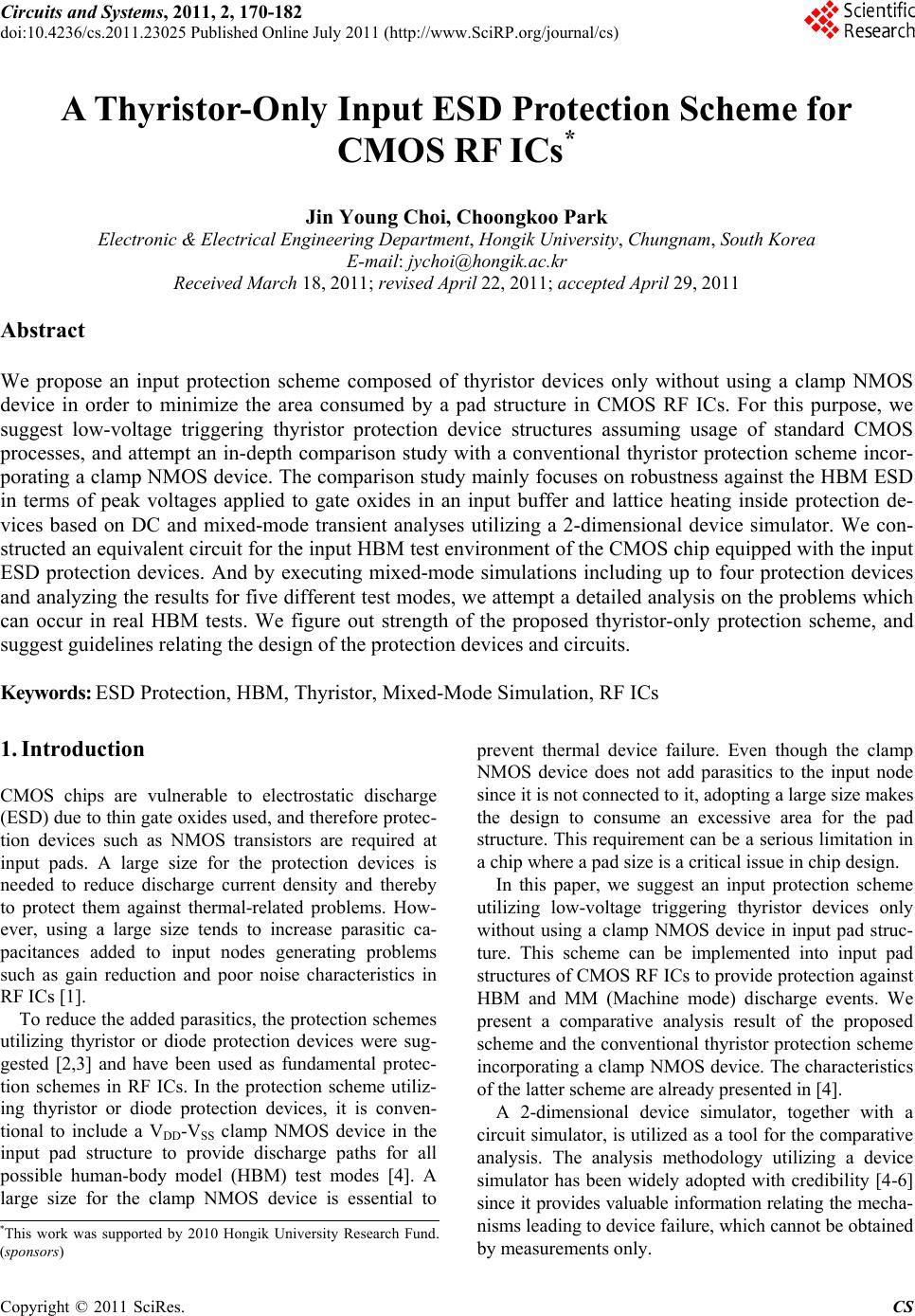
|