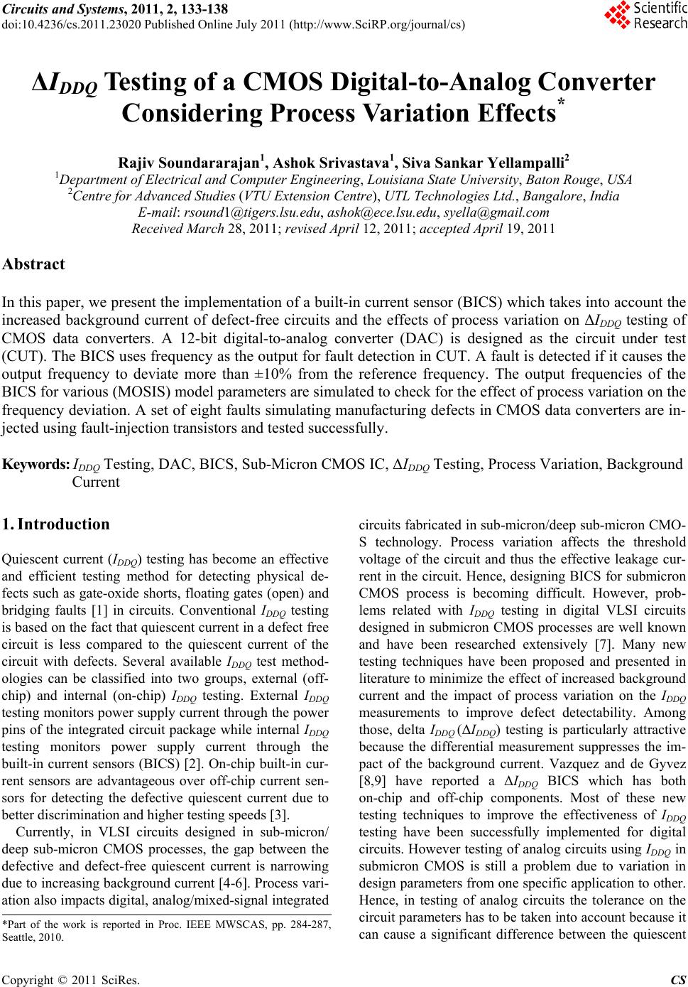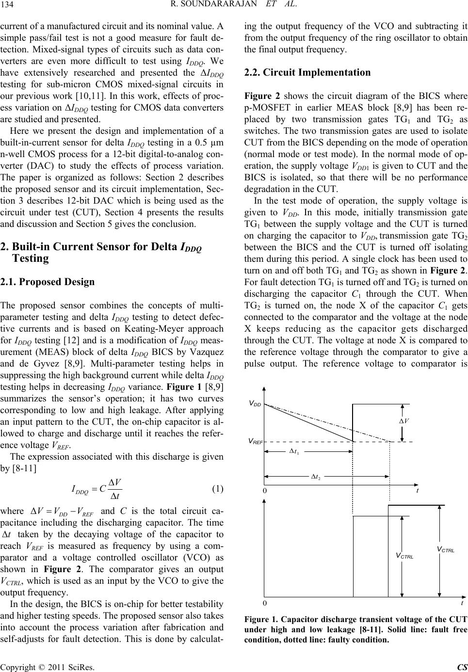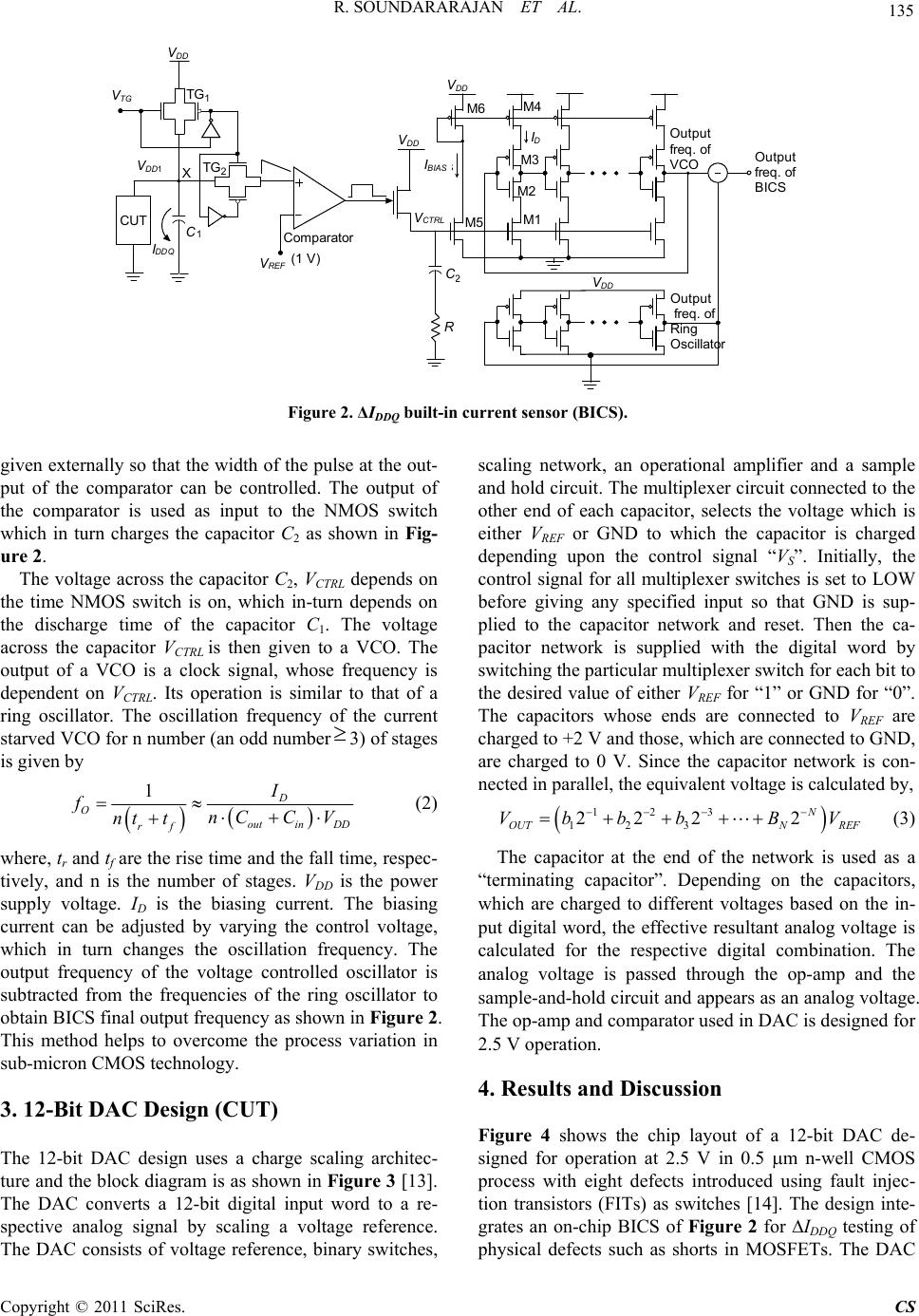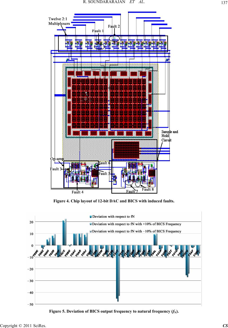
R. SOUNDARARAJAN ET AL.
Copyright © 2011 SciRes. CS
138
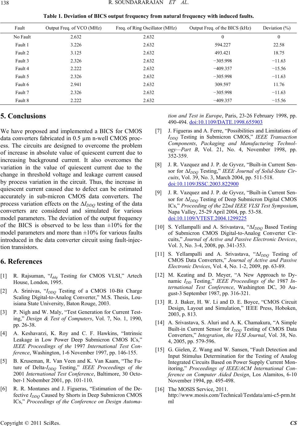
Table 1. Deviation of BICS output frequency from natural frequency with induced faults.
Fault Output Freq. of VCO (MHz) Freq. of Ring Oscillator (MHz) Output Freq. of the BICS (kHz) Deviation (%)
No Fault 2.632 2.632 0 0
Fault 1 3.226 2.632 594.227 22.58
Fault 2 3.125 2.632 493.421 18.75
Fault 3 2.326 2.632 −305.998 −11.63
Fault 4 2.222 2.632 −409.357 −15.56
Fault 5 2.326 2.632 −305.998 −11.63
Fault 6 2.941 2.632 309.597 11.76
Fault 7 2.326 2.632 −305.998 −11.63
Fault 8 2.222 2.632 −409.357 −15.56
5. Conclusions
We have proposed and implemented a BICS for CMOS
data converters fabricated in 0.5 µm n-well CMOS proc-
ess. The circuits are designed to overcome the problem
of increase in absolute value of quiescent current due to
increasing background current. It also overcomes the
variation in the value of quiescent current due to the
change in threshold voltage and leakage current caused
by process variation in the circuit. Thus, the increase in
quiescent current caused due to defect can be estimated
accurately in sub-micron CMOS data converters. The
process variation effects on the ΔIDDQ testing of the data
converters are considered and simulated for various
model parameters. The deviation of the output frequency
of the BICS is observed to be less than ±10% for the
model parameters and more than ±10% for various faults
introduced in the data converter circuit using fault-injec-
tion transistors.
6. References
[1] R. Rajsuman, “Iddq Testing for CMOS VLSI,” Artech
House, London, 1995.
[2] A. Srinivas, “IDDQ Testing of a CMOS 10-Bit Charge
Scaling Digital-to-Analog Converter,” M.S. Thesis, Lou-
isiana State University, Baton Rouge, 2003.
[3] P. Nigh and W. Maly, “Test Generation for Current Test-
ing,” Design & Test of Computers, Vol. 7, No. 1, 1990,
pp. 26-38.
[4] A. Keshavarzi, K. Roy and C. F. Hawkins, “Intrinsic
Leakage in Low Power Deep Submicron CMOS ICs,”
IEEE Proceedings of the 1997 International Test Con-
ference, Washington, 1-6 November 1997, pp. 146-155.
[5] B. Kruseman, R. Van Veen and K. Van Kaam, “The Fu-
ture of Delta-IDDQ Testing,” IEEE Proceedings of the
2001 International Test Conference, Baltimore, 30 Octo-
ber-1 Nobember 2001, pp. 101-110.
[6] R. R. Montanes and J. Figueras, “Estimation of the De-
fective IDDQ Caused by Shorts in Deep Submicron CMOS
ICs,” Proceedings of the Conference on Design Automa-
tion and Test in Europe, Paris, 23-26 February 1998, pp.
490-494. doi:10.1109/DATE.1998.655903
[7] J. Figueras and A. Ferre, “Possibilities and Limitations of
IDDQ Testing in Submicron CMOS,” IEEE Transaction
Components, Packaging and Manufacturing Technol-
ogy—Part B, Vol. 21, No. 4, November 1998, pp.
352-359.
[8] J. R. Vazquez and J. P. de Gyvez, “Built-in Current Sen-
sor for IDDQ Testing,” IEEE Journal of Solid-State Cir-
cuits, Vol. 39, No. 3, March 2004, pp. 511-518.
doi:10.1109/JSSC.2003.822900
[9] J. R. Vazquez and J. P. de Gyvez, “Built-in Current Sen-
sor for IDDQ Testing of Deep Submicron Digital CMOS
ICs,” Proceeding of the 22nd IEEE VLSI Test Symposium,
Napa Valley, 25-29 April 2004, pp. 53-58.
doi:10.1109/VTEST.2004.1299225
[10] S. Yellampalli and A. Srivastava, “ΔIDDQ Based Testing
of Submicron CMOS Digital-to-Analog Converter Cir-
cuits,” Journal of Active and Passive Electronic Devices,
Vol. 3, No. 3-4, 2008, pp. 341-353.
[11] S. Yellampalli and A. Srivastava, “ΔIDDQ Testing of
CMOS Data Converters,” Journal of Active and Passive
Electronic De vices, Vol. 4, No. 1-2, 2009, pp. 63-89.
[12] M. Keating and D. Meyer, “A New Approach to Dy-
namic IDD Testing,” IEEE Proceedings of the 1987 In-
ternational Test Conference, Washington DC, 30 Au-
gust-3 September 1987, pp. 316-321.
[13] R. J. Baker, H. W. Li and D. E. Boyce, “CMOS Circuit
Design, Layout and Simulation,” IEEE Press, Hoboken,
2003, p. 813.
[14] A. Srivastava, S. Aluri and A. K. Chamakura, “A Simple
Built-in Current Sensor for IDDQ Testing of CMOS Data
Converters,” Integration, the VLSI Journal, Vol. 38, No.
4, 2005, pp. 579-596.
[15] G. Gielen, Z. Wang and W. Sansen, “Fault Detection and
Input Stimulus Determination for the Testing of Analog
Integrated Circuits Based on Power Supply Current Mon-
itoring,” Proceedings of IEEE/ACM International Con-
ference on Computer Aided Design, Los Alamitos, 6-10
November 1994, pp. 495-498.
[16] The MOSIS Service, 2011.
http://www.mosis.com/Technical/Testdata/ami-c5-prm.ht
ml