 Circuits and Systems, 2011, 2, 112-120 doi:10.4236/cs.2011.23017 Published Online July 2011 (http://www.SciRP.org/journal/cs) Copyright © 2011 SciRes. CS A Fluctuation-Dissipation Model for Electrical Noise* Jose-Ignacio Izpura, Javier Malo Group of Microsystems and Electronic Materials, Universidad Politécnica de Madrid, Madrid, Spain E-mail: joseignacio.izpura@upm.es Received February 5, 2011; revised April 6, 2011; accepted April 13, 2011 Abstract This paper shows that today’s modelling of electrical noise as coming from noisy resistances is a non sense one contradicting their nature as systems bearing an electrical noise. We present a new model for electrical noise that including Johnson and Nyquist work also agrees with the Quantum Mechanical description of noisy systems done by Callen and Welton, where electrical energy fluctuates and is dissipated with time. By the two currents the Admittance function links in frequency domain with their common voltage, this new model shows the connection Cause-Effect that exists between Fluctuation and Dissipation of energy in time domain. In spite of its radical departure from today’s belief on electrical noise in resistors, this Complex model for electrical noise is obtained from Nyquist result by basic concepts of Circuit Theory and Thermo- dynamics that also apply to capacitors and inductors. Keywords: Admittance-Based, Noise Model, Fluctuation, Susceptance, Dissipation, Resistance 1. Introduction Current understanding of electrical noise in circuits con- siders shot and Johnson noises as different physical phe- nomena each with its own physical model, despite their deep connection found by some authors [1]. Considering electric current as carried by discrete electrons inde- pendently of one another, as Johnson did in vacuum de- vices to study their shot noise [2], this connection isn’t too surprising. What is a surprise, however, is that to- day’s works in this field tend to consider noise currents as carried by packets of electrons that, to our knowledge, hardly are found in ordinary matter. We mean proposals like [3] contending that electrical charge piling-up in a lonely resistance R generates shot noise, thus transgress- ing a Quantum-Mechanical result of [4]: the need for a Complex Admittance function to describe a noisy system. This transgression and that of Special Relativity that a null C shunting the R of a resistor endures [5], led us to review today’s modelling of electrical noise in this paper showing why the PSPICE simulator does not give the right noise of junction diodes [6] and what the effects are of today’s unawareness about the Susceptance that shunts the Conductance G = 1/R of any resistor we can make. The paper is organized as follows. In Section 2 we review the Partial Interpretation (PI) in use today of Johnson-Nyquist results that leads to a wrong modelling of electrical noise sometimes. Section 3 shows how to pass from this PI to an Advanced Model (AM) for elec- trical noise that agreeing with the laws of Physics, also allows a right modelling of this noise where the aforesaid PI fails. This passage is done in frequency domain by the familiar noise densities I Sf in 2 AHz and V Sf in 2 VHz. Section 4, however, considers the generation of electrical noise by Fluctuations and Dissipations of elec- trical energy in time domain, taking place in the Admit- tance of two-terminal devices like resistors and capaci- tors, no matter its physical structure. Some relevant con- clusions are drawn at the end. 2. Reviewing Current Model for Electrical Noise in Resistors To a first level, the Susceptance shunting the conductance 1GR of a resistor of resistance R is due to a capaci- tance Cd coming from the dielectric properties of the material used to fabricate this device, whose physical structure appears in Figure 1 and where the space be- tween two parallel plates (ohmic contacts) contains some material of dielectric permittivity ε and conductivity σ. We mean the Susceptance due to dd CR that each resistor bears in parallel with its R because the non-null dielectric relaxation time d of its inner material *Work supported by the Spanish CICYT under the MAT2010-18933 rojec , by the Comunidad Autónoma de Madrid through its IV-PRICIT Program, and by the European Regional Development Fund (FEDER).  J.-I. IZPURA ET AL. 113 [7]. Any stray capacitance as pF, typical of set-ups used in Low Frequency Noise (LFN) measure- ments [8], would be added to Cd. 0.5 stray C For conducting materials as n-doped Silicon or GaAs, d falls below the ps, thus giving very low Cd values: F for R = 1 k and d = 1 ps. This is why Cd and Cstray are considered irrelevant at frequencies f ≤ 1 MHz where LFN is found. This irrelevance that can be accepted numerically in most cases (e.g. when there are other Admittances in parallel), leads to the misconcep- tion underlying the aforesaid PI of the pioneering works of Johnson [9] and Nyquist [10]. This error is so deep-rooted in today’s research that reviewers of [3] were not ashamed of publishing a piling-up of electrical charge in a resistance devoid of capacitance C, which links electric charge and electric voltage 15 10 d C Qt vt . When a current it produces a change of dipolar charge as t passes, it builds a voltage Qit v that is linked with the charge variation at each instant by the Capacitance CQv . Thus, C = 0 between the two terminals of a resistor means that it could show an electrical voltage between them without electric charges acting as its source or, as we wrote in [5], its material having finite σ to offer a finite R with the structure of Figure 1, but having a null permittivity ε = 0 to offer Cd = 0, would allow an infinite speed for the electromag- netic wave, thus infringing Einstein’s Special Relativity. Besides this conflict with Physics, this PI of Nyquist work is hard to apply out of Thermal Equilibrium (TE) because [10] was done for TE. The footnote of Figure 4.11 of [11] summarizes the essence of this PI by this sentence: “Circuits elements and their noise models. Note that capacitors and inductors do not generate noise”. Figure 2 shows the circuits this PI uses to represent electrical noise in a resistor of resistance R, where a Conductance 1GR is shunted by a noise generator of density 4 I Sf kTR 2 AHz (Nyquist noise) for k being the Boltzmann constant. This leads to a noise density VI 2 Sf RSR 4f kT2 VHz (Johnson noise). Thus, a resistor is a noisy resistance [3] for this PI that uses the resistance R of a resistor in TE as a genera- tor of flat and V noises up to frequencies fQ 6.2 THz at room T, a quantum limit given in [10]. I Sf S f Let’s consider under this PI the circuit of Figure 3 with C = 0, where the voltage of a resistor of R = 100 k is sampled and feedback as a current by a feedback factor β = 1/R A/V. For this R = 100 k giving 4 V Sf kTR 1600 2 nVHz and 0. 16 I Sf 2 A Hz , the noise- less sampling and feedback of Figure 3 could be carried out quite well with today’s Operational Amplifiers [12] having input noise parameters as: 2 236 nVHz n e and 2 2 n i1fAHz. Accordingly to the PI in use today this negative feedback adds a noiseless R in parallel with the noisy R or resistor whose Nyquist noise I Sf is the input signal of this feedback circuit. Thus, the I Sf of the noisy R is the only source of noise in this circuit that, attenuated by the noiseless R, leads to kT VFB Sf R 2 VHz in it. This result agreeing with Figure 1. Physical structure of an elemental resistor whose ohmic contacts (shaded area) are the plates that enclose the parallel-plate capacitor of capacitance Cd = τd/R that allows to apply or to measure an electrical voltage between the terminals A and B of its resistance R. Figure 2. Parallel and series circuits that today’s Partial Interpretation (PI) of Johnson and Nyquist results uses to represent the electrical noise of a resistor (see text). (a) ( ) Figure 3. Feedback scheme used to show that today’s un- awareness about the role of Susceptance in electrical noise, doesn’t allow finding the “we ll known” kTC noise of the capacitor existing in this circuit. Copyright © 2011 SciRes. CS  114 J.-I. IZPURA ET AL. a “well know” one of this PI, namely: “the available noise power from a resistor of resistance R in TE at some T is Nf kTWHz”, deserves some attention. Because the noisy R and the noiseless R are driven by SfkTR VFB 2 VHz, they are dissipating Nf VFB SfRkTWHz, of course. Since the noisy R is out of TE due to its feedback, we find logical this lower dissipation than the 4kT W/Hz it dissipated in TE when it was driven by . What is less “logical” is the null dissipation R has in the equivalent circuit of Figure 2 with series connected with R, thus rais- ing doubts about the physical correctness of I Sf f V S V Sf , whose circuital correctness is well known. 2 I RSf To make some progress, let’s consider the noisy R shunted by C = 1 pF in Figure 3 to represent a pixel of an imaging device becoming charged by m electrons when a short packet of m/η photons is absorbed with quantum efficiency η < 1. “Short” means that photons are absorbed within a time interval tRC , where τ is the time constant of this R-C cell. Thus, a photon packet sets a charge of mq C in C (q is the elec- tron charge) and the voltage vmqC V appearing on R will be the aimed Signal on R whose power is: S = 2 mqCR W. Since C will discharge through R, the Signal readout would be done a short time d t after the photon absorption in order to find the aforesaid power S. Concerning Noise power N, the mean square noise voltage on R is the product of the Johnson noise 4 V Sf kTR V 2/Hz by the noise bandwidth N BW 2C of this circuit of cut-off frequency 12 C RC [13]: N = SV × BWN. This replaces the integration in f of to allow a fast reasoning using Signal to Noise ratios ( V Sf SN). Thus, the noise power in the pixel with- out feedback is: NkTRC W and its SN is: i SN 2 mqkTC , the ratio of the square charge signal in C C 2, divided by the square charge noise of C: kTC C2 [14]. To give some figures, the kT/C noise at room T (e.g. the square root of 2 mq kT of C = 1 pF is 64 Vrms. For a Signal ∆v = C) mq 6.4 mV we would have: C = 4 i10 SN 40 dB for the pixel with- out feedback. or With feedback, however, the BWN doubles due to R2 shunting the same C that this feedback in-phase with the output doesn’t vary [15]. From this double BWN with the noise power on R is: FB VFB SfkT 3. An Advanced Model for Electrical Noise in Resistors and Capacitors Because CQv links charge variations with volt- age ones related with electric fields storing energy be- tween terminals, C behaves as the reservoir of electrical energy whose thermal Fluctuations are observed as Johnson noise v(t) in resistors [7]. Using Thermodynam- ics, C sets the Degree of Freedom to store electrical en- ergy linked with the fluctuating v(t) in a resistor that a lonely resistance doesn’t have. Using Quantum Mechan- ics we will say that eingenstates of electrical energy hardly will be found in a lonely resistance unable to store it by some Susceptance in parallel or by a Reactance in series. Thus, a cogent model for electrical noise in resis- tors must handle Conductance 1GR together with Susceptance, and this also holds for noise modelling of capacitors in TE at some temperature T because they offer a similar Admittance [5]. It is worth noting that these ideas about noise in resis- tors are present in Figure 2 if one knows how to read its first circuit or which is the physical meaning of I Sf A2/Hz, a current-like power source proportional to the conductance it is driving. This I leads to 4kTG Sf V Sf 4kTR V 2/Hz, a power density that, being pro- portional to R while its bandwidth (note that Cd always exists) is proportional to 1/R, means that the mean square voltage noise has nothing to do with currents in R. Thus, the noise currents that 4Sf I re- presents must be currents inQ(t) orthogonal to noise currents inP(t) in G that always are in-phase with the voltage noise vn(t). This means currents inQ(t) always in quadrature with vn(t) flowing through a Susceptance shunting kTR 1GR . The compound device Nyquist used in [10] agrees with this feature of the AM for electrical noise we are going to show. This AM used to explain the 1/f excess noise of Solid-State devices [7] and the flicker noise of electron fluxes in vacuum ones [5], never has been described before at this level of detail, especially in time domain. The Susceptance or ability to store electrical energy our AM uses replacing the Transmission Line of [10], is the circuit element providing a Degree of Freedom to store electrical energy liable to fluctuate thermally in the device. These Fluctuations giving rise to the Johnson noise of resistors, don’t take place in R, but in its Sus- ceptance that must be capacitive because the flat 4 V Sf kTR V 2/Hz found by Johnson at low f [9] is not possible for an inductive Susceptance with Fluctua- tions of energy of finite power. To make easier the pas- sage from the PI to our AM let’s consider the electrical noise of a two-terminal circuit that can be reduced to a capacitance C at high f. The equipartition value for one R N2RCkT W. Since the Signal power on R doesn’t change because C doesn’t vary, the (SN) of the pixel with feedback would be doubled, a result well worth patenting provided it was true. Unfortunately, this noise modelling is wrong as we will show in the next Section. Copyright © 2011 SciRes. CS  J.-I. IZPURA ET AL. 115 Degree of Freedom applies to C in this case [14] and this gives the mean square voltage noise of C in TE from this equality: 22 11 22 kT kTCv tv tC (1) thus showing that the mean square voltage of noise has nothing to do with currents in R as we concluded previ- ously from Circuit Theory and why this is so. Because (1) gives the kTC noise of capacitive de- vices that doesn’t depend on the R that shunts C [13,14], let us consider the noise of the BAT85 Schottky diode of [6] whose PSPICE model appears in Appendix I. Due to its CJ0 = 11.1 pF, the kTC noise of this diode at room T is: 2 vt = 3.7 10–10 V2 or 19.3 Vrms. From its saturation current Isat = 211.7 nA and the ideality factor n = 1.016 of its i-v curve, CJ0 is shunted in TE by a resis- tance 1 00v dTsat riv nVI = 124.1 k, where T VkTq is the thermal voltage. Following our AM, the room T noise density of this diode at low f must be: V 2/Hz in TE because this is the value giving 04 VAM d S kTr 2 vt = 0 kT C in CJ0 to fulfil (1). There- fore, is this low-pass, Lorentzian spectrum: VAM Sf 0 2 0 00 1 42 21 121 d VAM J dJ c kTr f kT Sf C frC c (2) that integrated from to gives 0ff 2 vt = 0 kT C as it must be by Equipartition. Using PSPICE we have obtained the i-v curve of this diode shown in Figure 4 with a logarithmic axis to show its exponential character. Besides the simulated i-v we also present (by dots) the i-v solely due to thermoionic current represented by this equation: 9 3 exp 1 211.7 10exp1 1.01625.8510 sat T v iI nV v (3) The superposition of the two curves shows that cur- rents through R1 = 36 M used by PSPICE to get a better fitting in reverse mode (see Appendix I), are negligible. The inset of Figure 4 shows the i-v curve with linear axis in the region (v 0) where a resistance R*(v = 0) = 123.7 k can be found. This R* is: R* = 010 1dd rRrRr 0d Vrms. This SVPI(0) being 24.6 dB below SVAM(0) = 4kTR* . Curve a) of Figure 5 is the PSPICE gives for this diode in TE (i = 0 in the inset of Figure 5), whose flat SVPI(0) = 171.5 dB at low f means 1.13 Vrms noise in this diode whereas our AM states that it will be 19.3 = 146.9 dB, is a 292 times lower noise that PSPICE gives because it considers (as the aforesaid PI) that the only source of noise in the diode at v = 0 is R1 = 36 M, whose Nyquist noise V Sf 1 4 I Sf kTR drives the paral- lel circuit of rd0, R1 ans a low-pass spec- trum of amplitude SVPI (0) = d CJ0. This give2 * 1 4kTRR V 2/Hz at low f that is R1/R* times lower t0) = 4kTR* that our AM states to keep the han the SVAM( 0 kT C noise of 0 C shunted by R*. Since 10 1 log .6RR dB, this plains why today’s PI ofils to give a well known * 24 Nyquist result fa ex- kTC noise. Concerning circuit elements, PSPICE conshem perfectly as it is shown by the cut-off frequency fc = ider t * 0 12J RC = 115.6 kHz of curve a in Figure 5. Taking advantage of the correctness of the fc PSP gi ICE ves, we have simulated this diode out of TE, under a forward current i = Isat. The noise spectrum thus obtained is curve b of Figure 5, whose fc = 222.4 kHz comes from the low dynamical resistance of the diode under this forward bias: rd (i = Isat) = rdfw = 62 k, and its similar junction capacitance (slightly higher with the voltage v = 18.2 mV set by this i = Isat biasing the diode). Note that while the diode capacitance varies slightly for such a small voltage, the diode resistance varies as: exp(v/nVT) BAT85 Figure 4. Current-voltage (i-v) characteristics of the Schottky diode obtained by PSPICE (line) and its ther- moionic values (dots) given by (3) (see text). 150 175 200 Figure 5. Noise densities SV(f) obtained by PSPICE for the BAT85 Schottky diode at room T: a) without bias (Thermal Equilibrium, i = 0) and b) under forward bias (i = Isat). Curve a) does not give the kTC noise of its junction ca- pacitance (see text). Copyright © 2011 SciRes. CS  116 B tha J.-I. IZPURA ET AL. [7]. The SVSim(0) = 155.8 dt PSPICE gives at low f for i = I is the sho sat t noise of the net current i converted to voltage noise on rdfw = 62 k: 10 log(2qIsat rdfw 2) = 155.8 dB. This noise is 7.7 dB below SVAM(0) = (3/2)4kTrdfw = 148.1 dB that our AM will give for this case out of TE in the next Section. Considering that to deal with shot noise one has to take all the independent currents, not its net value [6], and that a net i = Isat is: i = (+2Isat) + (Isat), see (3), we have: SI (f)= 2q(Isat + 2Isat) A2/Hz that converted to SV on rdfw gives: 10 log(6qIsat 2 dfw r) = 151 dB. This improvement of the PSPICE’s prediction appears “converting” shot noise accordingly to a procedure that works fine in TE, where a net i = 0 = (+Isat) + (Isat) leads to: I Sf = 2q(Isat + Isat) that converted to SV on R* gives: SV(0) = 10 log[4qIsat (R*)2] (e.g. SV(0) = 146.8 dB) whih is similar to SVAM(0) = 4kTR* = 146.9 dB predicted by our AM. As it is shown in [5,7], this “conversion” by the square of a resistance fails out of TE [5,7] as we c 0 will see in the next Section linked with the meaning of Resistance in time domain. A proof favouring our AM that doesn’t need this advanced knowledge can be given from a paradox we had in previous Section where a negative feedback seemed to improve the S/N of the pixel of Fig- ure 3 accordingly to the PI in use today. Following our AM, however, the kT/C noise of C must be kept by tak- ing the low f noise density on R* as: SVAM(0) = 4kTR*, where R* is the resistance shunting C no matter its origin. If R* = R in the pixel without feedback we have: SVAM(0) = 4kTR V 2/Hz and when feedback makes R* = R/2, the noise is: SVAM(0) = 4kTR/2 V2/Hz, always keeping the kT/C noise of C. This keeps the noise power on R: NFB = kT/(RC) W and therefore, this negative feedback doesn’t improve the S/N as it is “well known”. When v is negative and few times VT, an interesting situation appears because the diode current becomes i Isat that, accordingly to the PI today in use, is a source of “shot” noise I Sf 2q(Isat) A2/Hz that converted to voltage noise (V2/Hz) by 2 d rv will track the exp(v/nVT) variation of rd(v) for CJ(v) constant. This is shown in Figure 6(a) by the noise spectra PSPICE gives for the diode biased by three reverse currents ia, ib and ic that set va = 3nVT, vb = 4nVT and vc = 5nVT in the diode respectively. To study the noise of the diode alone, R1 was removed from the PSPICE model. Due to the factor e 2.718… dividing rd (v) as we go from curve a) to curve b) of Figure 6(a), the bandwidth decreases by e whereas their low f value increases by e2. This gives Figure 6(a) looking like the picture represent- ing the Gain × Bandwidth conservation of Operational Amplifiers with resistive feedback. The results of our AM for these cases will be discussed in the next Section. 100 120 140 160 (a) 100 120 140 160 (b) Figure 6. (a) Noise densities S(f) obtained by PSPICE for the BAT85 Schottky diode aom T for three reverse cur- Dissipations of Electrical Energy in Time Be nusoidal components (Fourier synthesis) we will use en terminals of a noisy device will come fro V t ro rents (see text); (b) Noise densities SV(f) obtained by our Fluctuation-Dissipation model for electrical noise. 4. Electrical Noise as Fluctuations and cause an arbitrary voltage noise v(t) can be built from si sinusoidal noise voltages vn(t) and currents in(t) except otherwise stated. Being Conductance G(f) the ratio be- tween sinusoidal current and voltage mutually in-phase at frequency f, it doesn’t distinguish “ohmic” resistances of resistors from “non-ohmic” ones due to feedback or to junctions for example, because all of them dissipate power by Conduction Currents (CC) in phase with their voltage. To work with a parallel circuit let’s use the Ad- mittance function Y(jω) = G(ω) + jB(ω), whose Real part is Conductance G(ω) and whose Imaginary part is Sus- ceptance B(ω), where ω is the angular frequency ω = 2f and j is the imaginary unit indicating a 90˚ phase shift (orthogonality or null mean overlap in time for sinusoi- dal signals). From the meaning of Y(jω), a voltage noise vn(t) ob- served betwe m a current in-phase with vn(t) through G = 1/R* and from a current in-quadrature through B(ω). G = 1/R* means that we will use a Conductance that is independ- ent of f as it uses to happen in the device resistor at low f, because at high f it becomes a capacitor due to τd [7]. Figure 7 shows the circuit our AM uses for the electrical noise of resistors and capacitors in TE. Although it re- minds the parallel one of Figure 2, it has C = Cd + Cstray Copyright © 2011 SciRes. CS 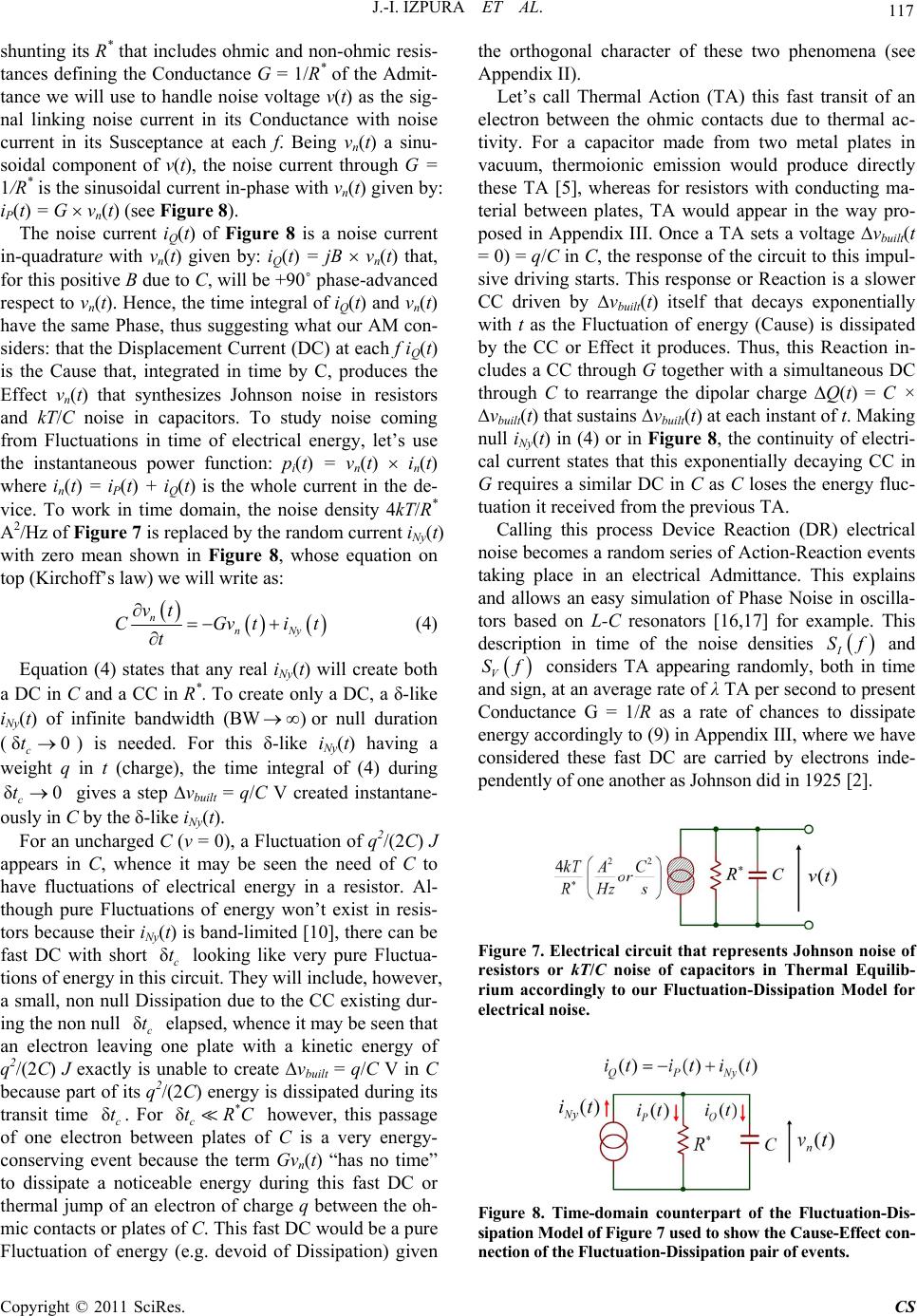 J.-I. IZPURA ET AL. 117 y: iQ(t) = jB vn(t) that, fo shunting its R* that includes ohmic and non-ohmic resis- tances defining the Conductance G = 1/R* of the Admit- tance we will use to handle noise voltage v(t) as the sig- nal linking noise current in its Conductance with noise current in its Susceptance at each f. Being vn(t) a sinu- soidal component of v(t), the noise current through G = 1/R* is the sinusoidal current in-phase with vn(t) given by: iP(t) = G vn(t) (see Figure 8 ). The noise current iQ(t) of Figure 8 is a noise current in-quadrature with vn(t) given b r this positive B due to C, will be +90˚ phase-advanced respect to vn(t). Hence, the time integral of iQ(t) and vn(t) have the same Phase, thus suggesting what our AM con- siders: that the Displacement Current (DC) at each f iQ(t) is the Cause that, integrated in time by C, produces the Effect vn(t) that synthesizes Johnson noise in resistors and kT/C noise in capacitors. To study noise coming from Fluctuations in time of electrical energy, let’s use the instantaneous power function: p i(t) = vn(t) i n(t) where in(t) = iP(t) + iQ(t) is the whole current in the de- vice. To work in time domain, the noise density 4kT/R* A2/Hz of Figure 7 is replaced by the random current iNy(t) with zero mean shown in Figure 8, whose equation on top (Kirchoff’s law) we will write as: n nN vt CGvti t y t (4) Equation (4) states that any real iNy(t) w a DC in C and a CC in R*. To create only a DC, a -like i For a e seen the need of C to ha ve use the term en the ohmic contacts due to thermal ac- tiv eaction events ta ill create both Ny(t) of infinite bandwidth (BW) or null duration (0 c t) is needed. For this -like iNy(t) having a weight q in t (charge), the time inal of (4) during cgives a step vbuilt = q/C V created instantane- ously in C by the -like iNy(t). n uncharged C (v = 0), a Fluctuation of q2/(2C) J appears in C, whence it may b tegr 0t ve fluctuations of electrical energy in a resistor. Al- though pure Fluctuations of energy won’t exist in resis- tors because their iNy(t) is band-limited [10], there can be fast DC with short c t looking like very pure Fluctua- tions of energy in this circuit. They will include, however, a small, non null Disation due to the CC existing dur- ing the non null c t elapsed, whence it may be seen that an electron leaving one plate with a kinetic energy of q2/(2C) J exactly is unable to create vbuilt = q/C V in C because part of its q2/(2C) energy is dissipated during its transit time c t. For * c tRC however, this passage of one electron between plates of C is a very energy- conserving ent beca Gvn(t) “has no time” to dissipate a noticeable energy during this fast DC or thermal jump of an electron of charge q between the oh- mic contacts or plates of C. This fast DC would be a pure Fluctuation of energy (e.g. devoid of Dissipation) given the orthogonal character of these two phenomena (see Appendix II). Let’s call Thermal Action (TA) this fast transit of an electron betwe sip ity. For a capacitor made from two metal plates in vacuum, thermoionic emission would produce directly these TA [5], whereas for resistors with conducting ma- terial between plates, TA would appear in the way pro- posed in Appendix III. Once a TA sets a voltage vbuilt(t = 0) = q/C in C, the response of the circuit to this impul- sive driving starts. This response or Reaction is a slower CC driven by vbuilt(t) itself that decays exponentially with t as the Fluctuation of energy (Cause) is dissipated by the CC or Effect it produces. Thus, this Reaction in- cludes a CC through G together with a simultaneous DC through C to rearrange the dipolar charge Q(t) = C × vbuilt(t) that sustains vbuilt(t) at each instant of t. Making null iNy(t) in (4) or in Figure 8, the continuity of electri- cal current states that this exponentially decaying CC in G requires a similar DC in C as C loses the energy fluc- tuation it received from the previous TA. Calling this process Device Reaction (DR) electrical noise becomes a random series of Action-R king place in an electrical Admittance. This explains and allows an easy simulation of Phase Noise in oscilla- tors based on L-C resonators [16,17] for example. This description in time of the noise densities I Sf and V Sf considers TA appearing randomly, both in time and sign, at an average rate of λ TA per seconesent tance G = 1/R as a rate of chances to dissipate energy accordingly to (9) in Appendix III, where we have considered these fast DC are carried by electrons inde- pendently of one another as Johnson did in 1925 [2]. d to pr Conduc Figure 7. Electric al circuit that represents Johnson noise of resistors or kT/C noise of capacitors in Thermal Equilib- rium accordingly to our Fluctuation-Dissipation Model for electrical noise. Figure 8. Time-domain counterpart of the Fluctuation-Dis- sipation Model of Figure 7 used to show the Cause-Effect con- nection of the Fluctuation-Dissipation pair of events. Copyright © 2011 SciRes. CS  118 J.-I. IZPURA ET AL. This view of G as λ chances per second to dissipate en- ergy suggests the reason why the conversion A2/Hz 2 V/Hz by the square of a resistance fails for very high R values, as those found in [7] for the rd(v) of reverse-bi- ased junctions with tens of VT. The high noise voltages this conversion gives as R* would require “packets of electrons” passing together between terminals [5] that, contrarily to [3], we consider unlikely to occur in com- mon devices. This led us to abandon this conversion in [7] replacing it by the AM or Fluctuation-Dissipation Model (FDM) for electrical noise just described, which was used to explain two noises [5,7] that the PI of Nyquist result in use today is unable to explain. To use this FDM out of TE let’s consider the cases of the BAT85 diode whose PSPICE spectra appeared in Fi * gure 6(a). Recalling that for v = 0 the diode is in TE with λ TA/s due to its two opposed Isat, the rate of TA for i ≈ −Isat, will drop to λ/2 [5,7]. Since C only has half the charge noise power it had in TE, we don’t have to keep 2 vt = kT/C in C, but half this value. Particularizing (2) for these cases, we have: 2 0 2 0 2 12 d VAMOUT kTr v Sf 1 1 1 dJ c J c fr v Cv fv kT Cv f fv (5) Integrating (5) from f to f we obtain: 0 2 vt = 0 2J kTCv . Fi g (5) gure 6(s the th no in uform b) show e fc P ree ise spectra obtained usinwith thSPICE gave Figre 6(a). They a ladder of slope 1/f whose sum gives a 1/f noise spectrum over a band (fLO – fHI) such that: exp 53. IO HITTT fnVnVVThis means one decade of 1/f noise for a voltage span of 2.3VT (e.g. 60 mV at room T), being this the basis e 1/f noise synthesizer that appeared in [5,7] with this FDM for electrical noise based on Admittance. To end, let’s justify the 0 VAM S = (3/2) 4kTrdfw = 148.1 dB value we proposed in previous Section as the no I, r of th ise for the diode with i =ll curve b) of Fig- ure 5. Due to the Isat and +2Isat existing in this case, we have: 3(λ/2) TA/s in C or a charge noise power that is 3/2 times higher than the one required to keep the kT/C noise of C by λ TA/s in TE. This means that for i = Isat we don’t have to keep sat eca 2 vt = kT/C V 2 in C by using 4kTrdfw V 2/Hz as the low f value of (2). In- stead, we have to keep 3/2 times value, whence it can be seen the reason to write this 032 4 VAM dfw SkTr 6kT r . 5. Conclusions dfw The partial interpretation of Nyquist result today in use 1-D) noise model based on issipation that is incomplete. A 2-D noise model using al no ] L. Callegaro, “Unified Derivation of Johnson and Shot ions,” American Journal of Physics, Vol. , pp. 438-440. doi:10.1119/1.2174034 leads to a 1-Dimensional ( D a Complex Admittance to handle Fluctuation and Dissi- pation of electrical energy, not only excels the aforesaid 1-D model, but also studies electrical noise accordingly to its first Quantum Mechanical treatment due to Callen and Welton. In this Complex model, Fluctuations and Dissipations of electrical energy creating electrical noise form a random series of Cause/Effect pairs in time, each linked with an elemental charge noise of one electron. For this Complex model of electrical noise, 1/f “excess noise” in Solid State devices and flicker noise in ther- moionic emitters simply are consequences of therm ise that the 1-D noise model based on Dissipation is unable to explain. This Complex model also shows that the Johnson noise of resistors and the kT/C noise of ca- pacitors, both reflect the same power 4kT/R of charge noise in C2/s or A2/Hz, appearing thermally between two conductors separated by some finite distance in our physical world. The quantization of electrical noise that results leads to an easy explanation of Phase noise in resonant circuits of electronic oscillators. 6. References [1 Noise Express 74, No. 5, 2006 [2] J. B. Johnson, “The Schottky Effect in Low Frequency Circuits,” Physical Review, Vol. 26, No. 1, 1925, pp. 71-85. doi:10.1103/PhysRev.26.71 [3] G. Gomila, C. Pennetta, L. Reggiani, M. Sampietro, G. Ferrari and G. Bertuccio, “Shot Noise in Linear Macro- scopic Resistors,” Physical Review Letters, Vol. 92, 2004, Article ID: 226601. doi:10.1103/PhysRevLett.92.226601 [4] H. B. Callen and T. A. Welton, “Irreversibility and Gen- eralized Noise,” Physical Review, Vol. 83, No. 1, 1951, pp. 34-40. doi:10.1103/PhysRev.83.34 [5] J. I. Izpura, “On the Electrical Origin of Flicker Noise in Vacuum Devices,” IEEE Transactions on Instrumenta- tion and Measurement, Vol. 58, No. 10, 2009, pp. 3592-3601. doi:10.1109/TIM.2009.2018692 [6] J. I. Izpura and J. Malo, “Noise Tunability in Planar Junc- tion Diodes: Theory, Experiment and Additional Support by SPICE,” TAEE’2006 Conference, Madrid, July 2006. http://taee.euitt.upm.es/Congresosv2/2006/papers/2006S1 F02.pdf [7] J. I. Izpura, “1/f Electrical Noise in Planar Resistors: The Joint Effect of a Backgating Noise and an Instrumental Disturbance,” IEEE Transactions on Instrumentation and Measurement, Vol. 57, No. 3, 2008, pp. 509-517. doi:10.1109/TIM.2007.911642 Copyright © 2011 SciRes. CS 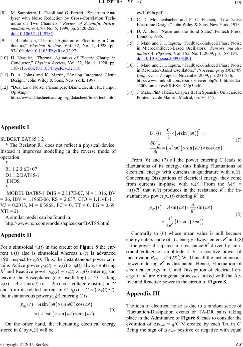 J.-I. IZPURA ET AL. Copyright © 2011 SciRes. CS 119 pp. 2520-2525. [8] M. Sampietro, L. Fasoli and G. Ferrari, “Spectrum Ana- lyzer with Noise Reduction by Cross-Correlation Tech- nique on Two Channels,” Review of Scientific I mentation, Vol. 70, No. 5, 1999, nstru- doi:10.1063/1.1149785 [9] J. B. Johnson, “Thermal Agitation of Electricity in Con- ductors,” Physical Review, Vol. 32, No. 1, 1928, pp. 97-109. doi:10.1103/PhysRev.32.97 [10] H. Nyquist, “Thermal Agitation of Electric Charge in Conductor,” Physical Review, Vol. 32, No. 1, 1928, pp. 110-113. doi:10.1103/PhysRev.32.110 [11] D. A. Johns and K. Martin, “Analog Integrated Cicuit acher and F. C. Fitchen, “Low Noise . Izpura, “Feedback-Induced Phase Noise gy/1169fa.pdf [13] C. D. Motchenb Electronic Design,” John Wiley & Sons, New York, 1973. [14] D. A. Bell, “Noise and the Solid State,” Pentech Press, London, 1985. [15] J. Malo and J. I in Microcantilever-Based Oscillators,” Sensors and Ac- tuators A: Physical, Vol. 155, No. 1, 2009, pp. 188-194. doi:10.1016/j.sna.2009.08.001 [16] J. Malo and J. I. Izpura, “Feedb Design,” John Wiley & Sons, New York, 1997. [12] “Dual Low Noise, Picoampere Bias Current, JFET Input Op Amp,” http://www.datasheetcatalog.org/datasheet/lineartechnolo ack-Induced Phase Noise i anish). Universidad ppendix I 5 1 2 r R1 does not reflect a physical device. stead it improves modelling in the reverse mode of AT85-1 DS 1 D(IS = 2.117E-07, N = 1.016, BV = = 1.196E-06, RS = 2.637, CJO = 1.114E-11, VJ = 0.2013, M = 0.3868, FC = 0, TT = 0, EG = 0.69, X A vn(t) in the circuit of Figure 8 the cur- sinusoidal whereas iQ(t) is advanced in Resonator-Based Oscillators,” Proceedings of DCIS’09 Conference, Zaragoza, November 2009, pp. 231-236. http://www.linkpdf.com/ebook-viewer.php?url=http://dc s2009.unizar.es/FILES/CR2/p5.pdf [17] J. Malo, PhD Thesis, Chapter III (in Sp Politecnica de Madrid, Madrid, pp. 70-145. A 2 2 () sin 2 sin cos E C UtAt UE Ct t t SUBCKT BAT8 * The Resisto (7) From (6) and (7) all the power entering C leads to flu ts in quadrature with vn(t). Concerning Dissipations of electrical energy, they come from currents in-phase with vn(t). From the iP(t) = vn(t)/R* that vn(t) produces in the resistance R stantaneous power piP(t) entering R* is: In operation. * R1 1 2 3.6E+07 D1 1 2 B ctuations of its energy, thus linking Fluctuations of electrical energy with curren .EN * *, the in- .MODEL BAT85- 36, IBV * 2 * sin sin 1cos2 2 iP pt Att R At R A (8) Contrarily to (6) whose mean value is null because energy enters and exits C, energy always enters R* and (8) is the power dissipated in a resistance R* TI = 2) A similar model can be found in: http://www.nxp.com/models/spicespar/BAT85.html ppendix II driven by sinu- soidal voltage of amplitude A V: a positive power of mean value Pavg = A2/(2R*) W. Thus all the instantaneous power entering R* is dissipated. Hence, electrical energy in C and Dissipation of electrical en- ergy in R* are orthogonal processes linked with the Ac- tiv built For a sinusoidal ent iP(t) also isr +90˚ respect to vn(t). Thus, the instantaneous power con- tains Active power piP(t) = vn(t) i P(t) always entering R* and Reactive power piQ(t) = vn(t) iQ(t) entering and leaving the Susceptance (e.g. oscillating) at 2f. Taking vn(t) = A sin(ωt) (ω = 2f) as a voltage existing on C and from its related current in C: iQ(t) = C (vn(t)/t), the instantaneous power piQ(t) entering C is: Fluctuation of e and Reactive power in the circuit of Figure 8. Appendix III The idea of electrical noise as due to a random series of Fluctuation-Dissipation events or TA-DR pairs taking place in the Admittance of Figure 8 leads to consider the evolution of vbuilt = q/C V created by each TA in C. Being the sign of v positive or negative with equal 2 sin cos sincos iQ pt AtACt Ct t (6) On the other hand, the fluctuating electrical energy stored in C by vn(t) will be:  J.-I. IZPURA ET AL. 120 ill be ull (v = 0). Taking λ/2 as the average rate of positive ate of TA is λ. For v = 0, each TA or harge fluctuation of one electron in C will set a Fluc- probability on average, the mean voltage in C w n TA, the average r C tuation UTA = q2/(2C) J in C. Once this Fluctuation is completed in a short transit time TA, its associated volt- age vbuilt = q/C starts to drive a slower DR or the Dissi- pation by R* of the UTA stored by the TA. Due to this, the initial vbuilt decays with a time constant = R*C as shown in Figure 9(a). The spectrum of this decay will look like the Lorentzian one of Figure 9(b), which is the Johnson noise v(t) of the circuit of Figure 7 coming from a random series of pulses like that of Figure 9(a), each following its own TA (Carson’s Theorem). Since the noise power N dissipated in R* (the kT/C noise of C divided by R*) has to dissipate the energy fluctuations of λ TAs per second on average, we have: 2 * *2* 24 2 2 kTqkT kT NRqq C RCq R (9) Equation (9) shows that the Resistance R* of a resistor or capacitor in TE is inversely proportional to the λ op- portunities per unit time it has to dissipate ene shows that the noise density 4kT/R* A2/Hz preserving the kT/C noise of C is the density of shot noise due to the λ TA’s per unit time taking place in this device. rgy. It also Thus, the shot noise 2qITA A 2/Hz of the current I λq associated to the λ TAs per unit time of this devi the source of its electrical noise, no matter if we call it Jo happens if we change the co his agrees with (9), where 10 times possible blockage by the conducting material between them. This is solved, however, by considering that a free electron in a Quantum State (QS) of the Conduction Band (CB) has a wavefunction extending over the whole material between plates. This would allow an electron to jump from a contact to this QS as soon as it is left empty by the electron that, occupying it previously, has been captured by the far contact (Collector). Thus, a QS or energy level of the CB would be a sort of tunnel for the fast transit of each electron between ohmic contacts cladding n-type semiconductor material for example. Used to electrons transiting between electrodes in vacuum devices that are collected a short transit time T after their emission, the above process looks reversed: an electron of the CB is captured by the Collector a short time T before another electron is emitted from the Emit- ter contact to the empty QS of the CB. Processes where electrons emitted from a contact to empty QS of the CB are subsequently captured by the other contact acting as a Collector of electrons are equally possible. TA = ce is hnson noise of its resistance R* or kT/C noise of its capacitance C. This deep connection between “shot” and Johnson noises (also found by other scientists [1]) is the charge noise existing in the capacitance C of a resistor or capacitor in TE due to its λ TA-DR pairs per unit time that are shown in Figure 10. Since each DR has a CC and a DC giving a charge fluctuation of q C each in C and they are uncorrelated in time due to their orthogonal character in f-domain, the mean square charge noise per second (charge noise power) existing in C due to DR is: 2(λq2) = 4kT/R* C2/s. This explains the alternative units used in Figure 7 to reveal neatly the same charge noise underlying Johnson and shot “noises”. It is worth studying what nducting material between plates in Figure 1 to reduce its R* to R*/10 while keeping the same ε. Since C does not vary its kT/C noise will remain, but the voltage de- cays of Figure 9(a) will be ten times faster, thus having a ten times broader spectrum (Figure 9(b)). Since the voltage vbuilt = q/C decays ten times faster with t, there must be ten times more TA (10λ) to sustain the same kT/C V 2 in time. T lower R* at the same T requires a 10 times higher rate of TA or 10 times more charge noise due to TA. Since this happens no matter the material we use, the presence of solid matter between contacts doesn’t change the nature of the TA in our FDM: a Charge Noise of one electron. Although single electrons jumping between plates in vacuum is well know [2], this is not so for electrons do- ing it between contacts in Solid-State devices due to their v n (t) 4 kTR 1/f 2 τ = CR * Frequency (a) (b) Figure 9. (a) Impulse response of the circuit of Figure 8 driven by current iNy(t) and taking v(t) as its output signal. (b) Bode plot (modulus) of the Lorentzian spectrum of v(t) mirroring the spectral energy content of the impulse shown in Figure 4. Figure 10. Charge noises in the contacts of a resistor or capacitor due to the (Thermal Action)/(Device Reaction) dynamics described in the te xt. Copyright © 2011 SciRes. CS
|