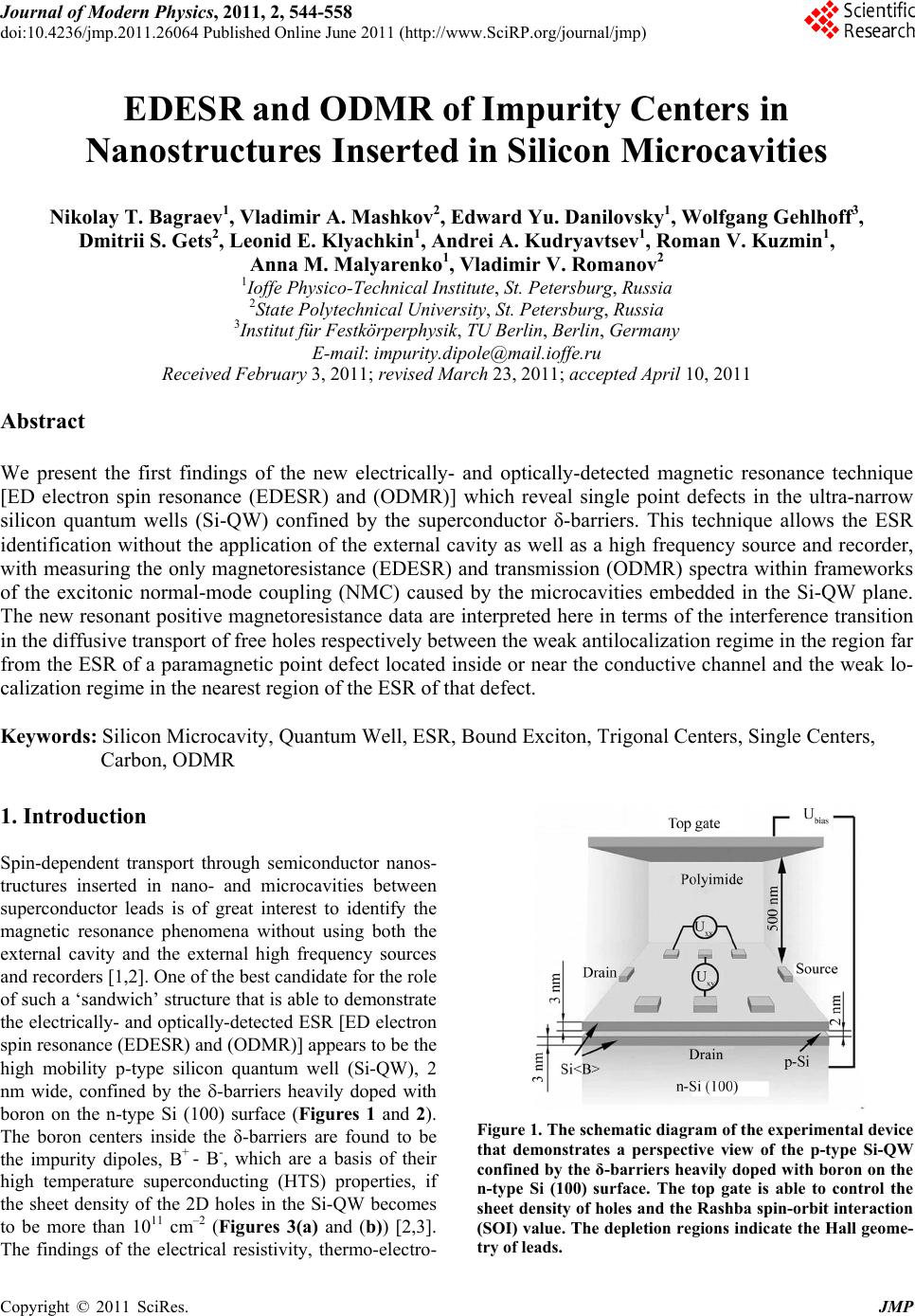
 Journal of Modern Physics, 2011, 2, 544-558 doi:10.4236/jmp.2011.26064 Published Online June 2011 (http://www.SciRP.org/journal/jmp) Copyright © 2011 SciRes. JMP EDESR and ODMR of Impurity Centers in Nanostructures Inserted in Silicon Microcavities Nikolay T. Bagraev1, Vladimir A. Mashkov2, Edward Yu. Danilovsky1, Wolfgang Gehlhoff3, Dmitrii S. Gets2, Leonid E. Klyachkin1, Andrei A. Kudryavtsev1, Roman V. Kuzmin1, Anna M. Malyarenko1, Vladimir V. Romanov2 1Ioffe Physico-Technical Institute, St. Petersburg, Russia 2State Polytechnical University, St. Petersburg, Russia 3Institut für Festkörperphysik, TU Berlin, Berlin, Germany E-mail: impurity.dipole@mail.ioffe.ru Received February 3, 2011; revised March 23, 2011; accepted April 10, 2011 Abstract We present the first findings of the new electrically- and optically-detected magnetic resonance technique [ED electron spin resonance (EDESR) and (ODMR)] which reveal single point defects in the ultra-narrow silicon quantum wells (Si-QW) confined by the superconductor δ-barriers. This technique allows the ESR identification without the application of the external cavity as well as a high frequency source and recorder, with measuring the only magnetoresistance (EDESR) and transmission (ODMR) spectra within frameworks of the excitonic normal-mode coupling (NMC) caused by the microcavities embedded in the Si-QW plane. The new resonant positive magnetoresistance data are interpreted here in terms of the interference transition in the diffusive transport of free holes respectively between the weak antilocalization regime in the region far from the ESR of a paramagnetic point defect located inside or near the conductive channel and the weak lo- calization regime in the nearest region of the ESR of that defect. Keywords: Silicon Microcavity, Quantum Well, ESR, Bound Exciton, Trigonal Centers, Single Centers, Carbon, ODMR 1. Introduction Spin-dependent transport through semiconductor nanos- tructures inserted in nano- and microcavities between superconductor leads is of great interest to identify the magnetic resonance phenomena without using both the external cavity and the external high frequency sources and recorders [1,2]. One of the best candidate for the role of such a ‘sandwich’ structure that is able to demonstrate the electrically- and optically-detected ESR [ED electron spin resonance (EDESR) and (ODMR)] appears to be the high mobility p-type silicon quantum well (Si-QW), 2 nm wide, confined by the -barriers heavily doped with boron on the n-type Si (100) surface (Figures 1 and 2). The boron centers inside the δ-barriers are found to be the impurity dipoles, B+ - B-, which are a basis of their high temperature superconducting (HTS) properties, if the sheet density of the 2D holes in the Si-QW becomes to be more than 1011 cm–2 (Figures 3(a) and (b)) [2,3]. The findings of the electrical resistivity, thermo-electro- Figure 1. The schematic diagram of the experimental device that demonstrates a perspective view of the p-type Si-QW confined by the δ-barriers heavily doped with boron on the n-type Si (100) surface. The top gate is able to control the sheet density of holes and the Rashba spin-orbit interaction (SOI) value. The depletion regions indicate the Hall geome- try of leads. 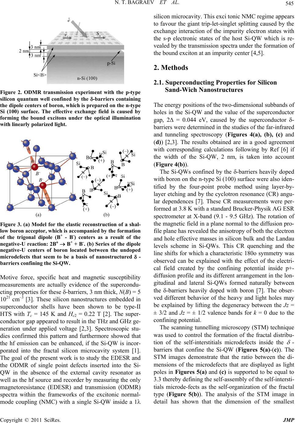 N. T. BAGRAEV ET AL. 545 Figure 2. ODMR transmission experiment with the p-type silicon quantum well confined by the -barriers containing the dipole centers of boron, which is prepared on the n-type Si (100) surface. The effective exchange field is caused by forming the bound excitons under the optical illumination with linearly polarized light. Figure 3. (a) Model for the elastic reconstruction of a shal- low boron acceptor, which is accompanied by the formation of the trigonal dipole (B+ - B-) centers as a result of the negative-U reaction: 2Bo B+ + B-. (b) Series of the dipole negative-U centers of boron located between the undoped microdefects that seem to be a basis of nanostructured - barriers confining the Si-QW. Motive force, specific heat and magnetic susceptibility measurements are actually evidence of the supercondu- cting properties for these -barriers, 3 nm thick, N(B) = 5 1021 cm–3 [3]. These silicon nanostructures embedded in superconductor shells have been shown to be type-II HTS with Tc = 145 K and Hc2 = 0.22 T [2]. The super- conductor gap appeared to result in the THz and GHz ge- neration under applied voltage [2,3]. Spectroscopic stu- dies confirmed this pattern and furthermore showed that the hf emission can be enhanced, if the Si-QW is incor- porated into the fractal silicon microcavity system [1]. The goal of the present work is to study the EDESR and the ODMR of single point defects inserted into the Si- QW in the absence of the external cavity resonator as well as the hf source and recorder by measuring the only magnetoresistance (EDESR) and transmission (ODMR) spectra within the frameworks of the excitonic normal- mode coupling (NMC) with a single Si-QW inside a 1 silicon microcavity. This exci tonic NMC regime appears to favour the giant trip-let-singlet splitting caused by the exchange interaction of the impurity electron states with the s-p electronic states of the host Si-QW which is re- vealed by the transmission spectra under the formation of the bound exciton at an impurity center [4,5]. 2. Methods 2.1. Superconducting Properties for Silicon Sand-Wich Nanostructures The energy positions of the two-dimensional subbands of holes in the Si-QW and the value of the superconductor gap, 2∆ = 0.044 eV, caused by the superconductor - barriers were determined in the studies of the far-infrared and tunneling spectroscopy (Figures 4(a), (b), (c) and (d)) [2,3]. The results obtained are in a good agreement with corresponding calculations following by Ref [6] if the width of the Si-QW, 2 nm, is taken into account (Figure 4(b)). The Si-QWs confined by the -barriers heavily doped with boron on the n-type Si (100) surface were also iden- tified by the four-point probe method using layer-by- layer etching and by the cyclotron resonance (CR) angu- lar dependences [7]. These CR measurements were per- formed at 3.8 K with a standard Brucker-Physik AG ESR spectrometer at X-band (9.1 - 9.5 GHz). The rotation of the magnetic field in a plane normal to the diffusion pro- file plane has revealed the anisotropy of both the electron and hole effective masses in silicon bulk and the Landau levels scheme in Si-QWs. This CR quenching and the line shifts for which a characteristic 180o symmetry was observed can be explained with the effect of the electri- cal field created by the confining potential inside p+- diffusion profile and its different arrangement in the lon- gitudinal and lateral Si-QWs formed naturally between the -barriers heavily doped with boron [7]. The obser- ved different behavior of the heavy and light holes may be explained by lifting the degeneracy between the Jz = ± 3/2 and Jz = ± 1/2 valence bands for k = 0 due to the confining potential. The scanning tunnelling microscopy (STM) technique was used to control the formation of the fractal distribu- tion of the self-interstitials microdefects inside the - barriers that confine the Si-QW (Figures 5(a)-(c)). The STM images demonstrate that the ratio between the di- mensions of the microdefects that are displayed as light poles in Figures 5(a) and (c) is supported to be equal to 3.3 thereby defining the self-assembly of the self-intersti- tials microde-fects as the self-organization of the fractal type (Figure 5(b)). The analysis of the STM image in detail has shown that the dimension of the smallest Copyright © 2011 SciRes. JMP 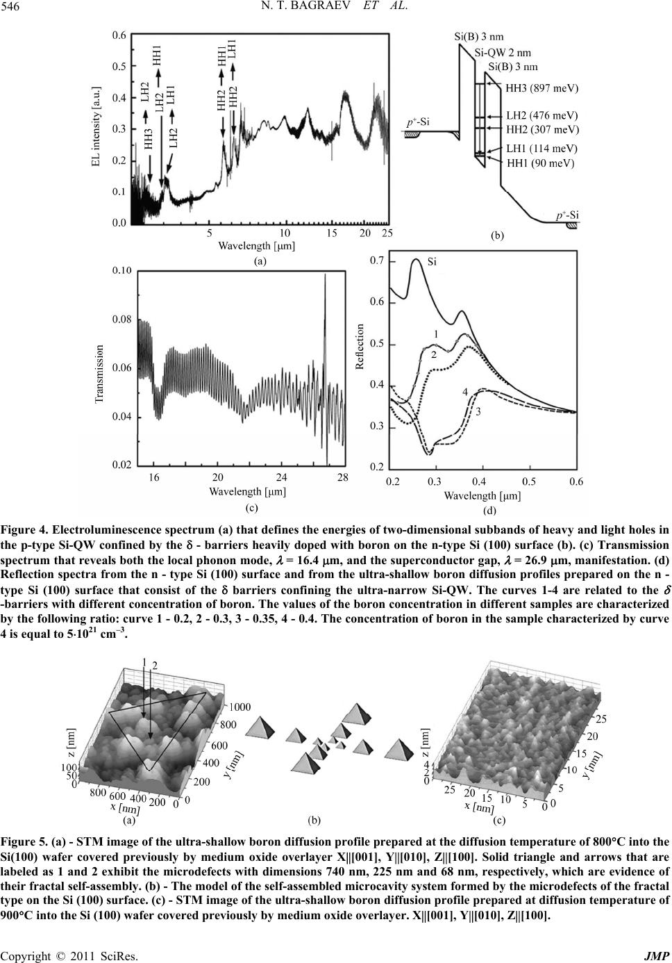 N. T. BAGRAEV ET AL. Copyright © 2011 SciRes. JMP 546 Figure 4. Electroluminescence spectrum (a) that defines the energies of two-dimensional subbands of heavy and light holes in the p-type Si-QW confined by the - barriers heavily doped with boron on the n-type Si (100) surface (b). (c) Transmission spectrum that reveals both the local phonon mode, = 16.4 m, and the superconductor gap, = 26.9 m, manifestation. (d) Reflection spectra from the n - type Si (100) surface and from the ultra-shallow boron diffusion profiles prepared on the n - type Si (100) surface that consist of the barriers confining the ultra-narrow Si-QW. The curves 1-4 are related to the -barriers with different concentration of boron. The values of the boron concentration in different samples are characterized by the following ratio: curve 1 - 0.2, 2 - 0.3, 3 - 0.35, 4 - 0.4. The concentration of boron in the sample characterized by curve 4 is equal to 51021 cm–3. Figure 5. (a) - STM image of the ultra-shallow boron diffusion profile prepared at the diffusion temperature of 800C into the Si(100) wafer covered previously by medium oxide overlayer X[001], Y[010], Z[100]. Solid triangle and arrows that are labeled as 1 and 2 exhibit the microdefects with dimensions 740 nm, 225 nm and 68 nm, respectively, which are evidence of their fractal self-assembly. (b) - The model of the self-assembled microcavity system formed by the microdefects of the fractal type on the Si (100) surface. (c) - STM image of the ultra-shallow boron diffusion profile prepared at diffusion temperature of 900C into the Si (100) wafer covered previously by medium oxide overlayer. X[001], Y[010], Z[100].  N. T. BAGRAEV ET AL. Copyright © 2011 SciRes. JMP 547 microdefect observed in fractal series, ~2 nm, is consis- tent with the parameters expected from the tetra- hedral model of the Si60 cluster (Figure 5(c)) [8]. Thus, the - barriers, 3 nm, heavily doped with boron, 5 × 1021 cm–3, represent really alternating arrays of the smallest undoped microdefects and doped dots with di- mensions restricted to 2 nm (Figure 5(c)). The value of the boron concentration determined by the secondary ion mass spectrometry (SIMS) method seems to indicate that each doped dot located between undoped microdefects contains two impurity atoms of boron. Since the boron dopants form shallow acceptor centers in the silicon lat- tice, such high concentration has to cause a metallic-like conductivity. Nevertheless, the angular dependences of the cyclotron resonance spectra demonstrate that the p- type Si-QW confined by the - barriers heavily doped with boron contains the high mobility 2D hole gas which is characterized by long momentum relaxation time of the heavy and light holes at 3.8 K, τ ≥ 5·10–10 s [7,9]. Thus, the momentum relaxation time of holes in the ul- tra-narrow Si-QW appeared to be longer than in the best metal-oxide-semiconductor (MOS) structures contrary to what might be expected from strong scattering by the heavily doped - barriers. This passive role of the - barriers between which the Si-QW is formed was quite surprising, when one takes into account the high level of their boron doping. To eliminate this contradiction, the ESR technique has been applied for the studies of the boron centers packed up in dots [9,10]. The angular de- pendences of the ESR spectra at different temperatures in the 3.8 ÷ 27 K range that reveal the trigonal symmetry of the boron dipole centers have been obtained with the same ESR spectrometer, the Brucker-Physik AG, at X- band (9.1 - 9.5 GHz), with the rotation of the magnetic field in the {110}-plane perpendicular to a {100}-interface (Bext = 0˚, 180˚ parallel to the Si-QW plane, Bext = 90˚ per- pendicular to the Si-QW plane) (Figures 6 (a)-(c) and (d)). No X-band ESR signals in the X-band are observed, if the Si-QW confined by the - barriers is cooled down in the external magnetic field (Bext) weaker than 0.22 T, with the persistence of the amplitude and the resonance field of the trigonal ESR spectrum as a function of the crystallo- graphic orientation and the magnetic field value during cooling down process at Bext ≥ 0.22 T (Figures 6(a)-(c)). With increasing temperature, the ESR line observed changes its magnetic resonance field position and disap- pears at 27 K (Figure 6(c)). The observation of the ESR spectrum is evidence of the fall in the electrical activity of shallow boron accep- tors contrary to high level of boron doping. Therefore, the trigonal ESR spectrum observed seems to be evi- dence of the dynamic magnetic moment that is induced by the exchange interaction between the small hole bipo- larons which are formed by the negative-U reconstruct- tion of the shallow boron acceptors, 2B0 B+ + B–, along the <111> crystallographic axis (Figure 3(a)) [7,10,11]. These small hole bipolarons localized at the dipole boron centers, B+ – B–, seem to undergo the singlet-triplet tran- sition in the process of the exchange interaction through the holes in the Si-QW thereby leading to the trigonal ESR spectrum (Figures 6(a)-( d)). Besides, the sublattice of the hole bipolarons located between the undoped mi- crodefects appears to define the one-electron band scheme of the - barriers as well as the transport properties for the 2D gas of holes in the Si-QW (Figures 4(b) and (d)) [10]. In order to determine the one-electron band scheme of the - barriers that confine the Si-QW, the reflection spectra R( ) were studied using an UV-VIS Specord M-40 spectrophotometer with an Ulbricht sphere for the reflectivity measurements [12]. Figure 4(d) shows the spectra of the reflection from the - barriers with diffe- rent concentration of boron. The decrease in R() com- pared with the data of the silicon single crystal and the drops in the position of the peaks at the wavelengths of = 354 and 275 nm are observed. The above peaks are related to the transitions between Γ and L valleys and in the vicinity of the point X in the Brillouin zone, with the former of the above peaks being assigned to the direct transition Γ’25 - Γ’2, whereas the latter peak is attributed to the transition X4 – X1. An analysis of the spectral de- pendence of the reflection coefficient shows that the pre- sence of microcavities formed by the self-assembled mi- crodefects with medium size reduces R( ) most pro- foundly in the short-wavelength region of the spectrum (200 - 300 nm). It follows from the comparison of R( ) with the STM data that the position of the minima in the reflection coefficient in the spectral dependence R( ) and the microcavity size are interrelated and satisfy the Bragg condition, x = /2 n, where x is the cavity size, is the wavelength, and n is the refractive index of silicon, n = 3.4. The R() drop in the position of the Γ’25 - Γ’2 and X4 – X1 transitions appears to be due to the formation of the wide-gap semiconductor layer with increasing the concentration of boron. These data substantiate the as- sumption noticed above that the role of the dot contain- ing the small hole bipolaron is to establish the band structure of the - barrier with the energy confinement more than 1.25 eV in both the conduction and the va- lence band of the Si-QW (Figure 4(d)). 2.2. GHz and THz Generation from Silicon Sandwich Nanostructures In order to identify the transfer of the small hole bipolar- rons as a possible mechanism of superconductivity, the 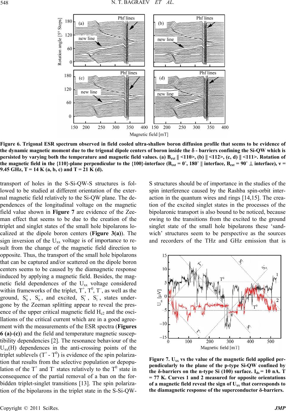 N. T. BAGRAEV ET AL. Copyright © 2011 SciRes. JMP 548 Figure 6. Trigonal ESR spectrum observed in field cooled ultra-shallow boron diffusion profile that seems to be evidence of the dynamic magnetic moment due to the trigonal dipole centers of boron inside the - barriers confining the Si-QW which is persisted by varying both the temperature and magnetic field values. (a) Bext <110>, (b) <112>, (c, d) <111>. Rotation of the magnetic field in the {110}-plane perpendicular to the {100}-interface (Bext = 0˚, 180˚ interface, Bext = 90˚ interface), ν = 9.45 GHz, T = 14 K (a, b, c) and T = 21 K (d). transport of holes in the S-Si-QW-S structures is fol- lowed to be studied at different orientation of the exter- nal magnetic field relatively to the Si-QW plane. The de- pendences of the longitudinal voltage on the magnetic field value shown in Figure 7 are evidence of the Zee- man effect that seems to be due to the creation of the triplet and singlet states of the small hole bipolarons lo- calized at the dipole boron centers (Figure 3(a)). The sign inversion of the Uxx voltage is of importance to re- sult from the change of the magnetic field direction to opposite. Thus, the transport of the small hole bipolarons that can be captured and/or scattered on the dipole boron centers seems to be caused by the diamagnetic response induced by applying a magnetic field. Besides, the mag- netic field dependences of the Uxx voltage considered within frameworks of the triplet, T+, T0, T–, as well as the ground, 0, 0, and excited, 1 S, 1, states under- gone by the Zeeman splitting appear to reveal the pres- ence of the upper critical magnetic field Hc2 and the osci- llations of the critical current which are in a good agree- ment with the measurements of the ESR spectra (Figures 6 (a)-(c)) and the field and temperature magnetic suscep- tibility dependencies [2]. The resonance behaviour of the Uxx(H) dependences in the anti-crossing points of the triplet sublevels (T+ - T0) is evidence of the spin polariza- tion that results from the selective population or depopu- lation of the T+ and T- states relatively to the T0 state in consequence of the partial removal of a ban on the for- bidden triplet-singlet transitions [13]. The spin polariza- tion of the bipolarons in the triplet state in the S-Si-QW- S structures should be of importance in the studies of the spin interference caused by the Rashba spin-orbit inter- action in the quantum wires and rings [14,15]. The crea- tion of the excited singlet states in the processes of the bipolaronic transport is also bound to be noticed, because owing to the transitions from the excited to the ground singlet state of the small hole bipolarons these ‘sand- wich’ structures seem to be perspective as the sources and recorders of the THz and GHz emission that is SS S T0 Figure 7. Uxx vs the value of the magnetic field applied per- pendicularly to the plane of the p-type Si-QW confined by the δ-barriers on the n-type Si (100) surface. Ids = 10 nA. T = 77 K. Curves 1 and 2 measured for opposite orientations of a magnetic field reveal the sign of Uxx that corresponds to the diamagnetic response of the superconductor δ-barriers. 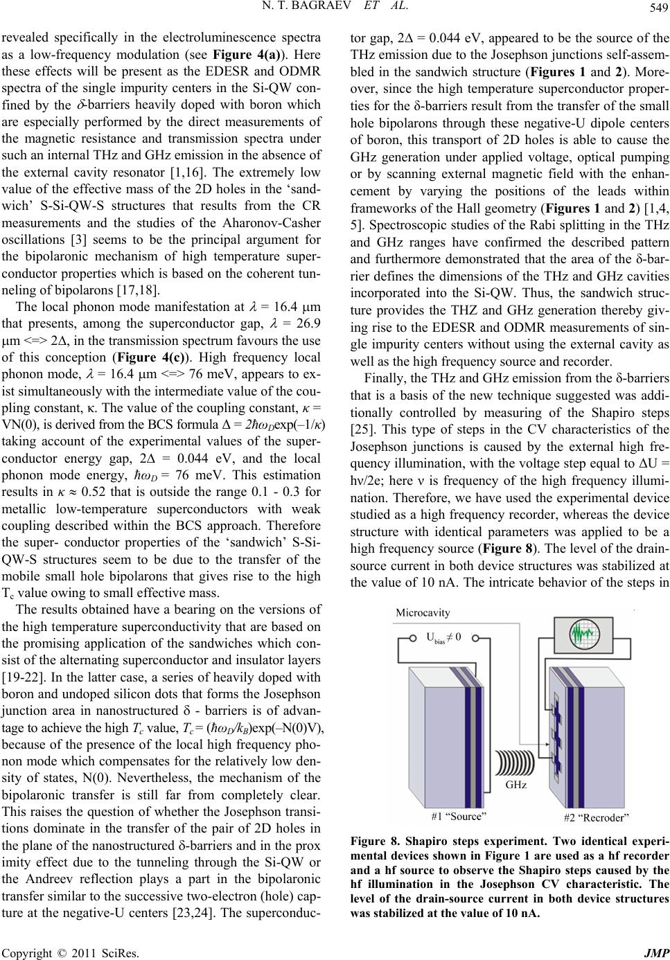 N. T. BAGRAEV ET AL. 549 revealed specifically in the electroluminescence spectra as a low-frequency modulation (see Figure 4(a)). Here these effects will be present as the EDESR and ODMR spectra of the single impurity centers in the Si-QW con- fined by the -barriers heavily doped with boron which are especially performed by the direct measurements of the magnetic resistance and transmission spectra under such an internal THz and GHz emission in the absence of the external cavity resonator [1,16]. The extremely low value of the effective mass of the 2D holes in the ‘sand- wich’ S-Si-QW-S structures that results from the CR measurements and the studies of the Aharonov-Casher oscillations [3] seems to be the principal argument for the bipolaronic mechanism of high temperature super- conductor properties which is based on the coherent tun- neling of bipolarons [17,18]. The local phonon mode manifestation at = 16.4 m that presents, among the superconductor gap, = 26.9 m <=> 2, in the transmission spectrum favours the use of this conception (Figure 4(c)). High frequency local phonon mode, = 16.4 m <=> 76 meV, appears to ex- ist simultaneously with the intermediate value of the cou- pling constant, κ. The value of the coupling constant, κ = VN(0), is derived from the BCS formula Δ = 2ħωDexp(–1/κ) taking account of the experimental values of the super- conductor energy gap, 2 = 0.044 eV, and the local phonon mode energy, ħωD = 76 meV. This estimation results in κ 0.52 that is outside the range 0.1 - 0.3 for metallic low-temperature superconductors with weak coupling described within the BCS approach. Therefore the super- conductor properties of the ‘sandwich’ S-Si- QW-S structures seem to be due to the transfer of the mobile small hole bipolarons that gives rise to the high Tc value owing to small effective mass. The results obtained have a bearing on the versions of the high temperature superconductivity that are based on the promising application of the sandwiches which con- sist of the alternating superconductor and insulator layers [19-22]. In the latter case, a series of heavily doped with boron and undoped silicon dots that forms the Josephson junction area in nanostructured - barriers is of advan- tage to achieve the high Tc value, Tc = (ħωD/kB)exp(–N(0)V), because of the presence of the local high frequency pho- non mode which compensates for the relatively low den- sity of states, N(0). Nevertheless, the mechanism of the bipolaronic transfer is still far from completely clear. This raises the question of whether the Josephson transi- tions dominate in the transfer of the pair of 2D holes in the plane of the nanostructured -barriers and in the prox imity effect due to the tunneling through the Si-QW or the Andreev reflection plays a part in the bipolaronic transfer similar to the successive two-electron (hole) cap- ture at the negative-U centers [23,24]. The superconduc- tor gap, 2 = 0.044 eV, appeared to be the source of the THz emission due to the Josephson junctions self-assem- bled in the sandwich structure (Figures 1 and 2). More- over, since the high temperature superconductor proper- ties for the δ-barriers result from the transfer of the small hole bipolarons through these negative-U dipole centers of boron, this transport of 2D holes is able to cause the GHz generation under applied voltage, optical pumping or by scanning external magnetic field with the enhan- cement by varying the positions of the leads within frameworks of the Hall geometry (Figures 1 and 2) [1,4, 5]. Spectroscopic studies of the Rabi splitting in the THz and GHz ranges have confirmed the described pattern and furthermore demonstrated that the area of the δ-bar- rier defines the dimensions of the THz and GHz cavities incorporated into the Si-QW. Thus, the sandwich struc- ture provides the THZ and GHz generation thereby giv- ing rise to the EDESR and ODMR measurements of sin- gle impurity centers without using the external cavity as well as the high frequency source and recorder. Finally, the THz and GHz emission from the δ-barriers that is a basis of the new technique suggested was addi- tionally controlled by measuring of the Shapiro steps [25]. This type of steps in the CV characteristics of the Josephson junctions is caused by the external high fre- quency illumination, with the voltage step equal to ΔU = hν/2e; here ν is frequency of the high frequency illumi- nation. Therefore, we have used the experimental device studied as a high frequency recorder, whereas the device structure with identical parameters was applied to be a high frequency source (Figure 8). The level of the drain- source current in both device structures was stabilized at the value of 10 nA. The intricate behavior of the steps in Figure 8. Shapiro steps experiment. Two identical experi- mental devices shown in Figure 1 are used as a hf recorder and a hf source to observe the Shapiro steps caused by the hf illumination in the Josephson CV characteristic. The level of the drain-source current in both device structures was stabilized at the value of 10 nA. Copyright © 2011 SciRes. JMP 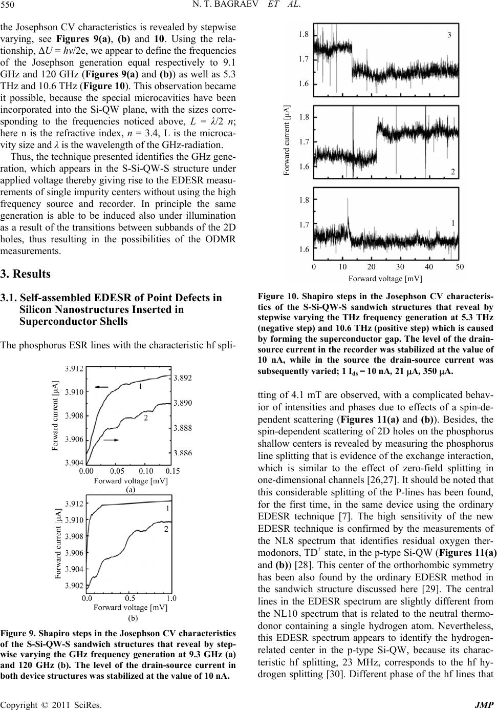 550 N. T. BAGRAEV ET AL. the Josephson CV characteristics is revealed by stepwise varying, see Figures 9(a), (b) and 10. Using the rela- tionship, ΔU = hν/2e, we appear to define the frequencies of the Josephson generation equal respectively to 9.1 GHz and 120 GHz (Figures 9(a) and (b)) as well as 5.3 THz and 10.6 THz (Figure 10). This observation became it possible, because the special microcavities have been incorporated into the Si-QW plane, with the sizes corre- sponding to the frequencies noticed above, L = λ/2 n; here n is the refractive index, n = 3.4, L is the microca- vity size and λ is the wavelength of the GHz-radiation. Thus, the technique presented identifies the GHz gene- ration, which appears in the S-Si-QW-S structure under applied voltage thereby giving rise to the EDESR measu- rements of single impurity centers without using the high frequency source and recorder. In principle the same generation is able to be induced also under illumination as a result of the transitions between subbands of the 2D holes, thus resulting in the possibilities of the ODMR measurements. 3. Results 3.1. Self-assembled EDESR of Point Defects in Silicon Nanostructures Inserted in Superconductor Shells The phosphorus ESR lines with the characteristic hf spli- Figure 9. Shapiro steps in the Josephson CV characteristics of the S-Si-QW-S sandwich structures that reveal by step- wise varying the GHz frequency generation at 9.3 GHz (a) and 120 GHz (b). The level of the drain-source current in both device structures was stabilized at the value of 10 nA. Figure 10. Shapiro steps in the Josephson CV characteris- tics of the S-Si-QW-S sandwich structures that reveal by stepwise varying the THz frequency generation at 5.3 THz (negative step) and 10.6 THz (positive step) which is caused by forming the superconductor gap. The level of the drain- source current in the recorder was stabilized at the value of 10 nA, while in the source the drain-source current was subsequently varied; 1 Ids = 10 nA, 21 A, 350 A. tting of 4.1 mT are observed, with a complicated behav- ior of intensities and phases due to effects of a spin-de- pendent scattering (Figures 11(a) and (b)). Besides, the spin-dependent scattering of 2D holes on the phosphorus shallow centers is revealed by measuring the phosphorus line splitting that is evidence of the exchange interaction, which is similar to the effect of zero-field splitting in one-dimensional channels [26,27]. It should be noted that this considerable splitting of the P-lines has been found, for the first time, in the same device using the ordinary EDESR technique [7]. The high sensitivity of the new EDESR technique is confirmed by the measurements of the NL8 spectrum that identifies residual oxygen ther- modonors, TD+ state, in the p-type Si-QW (Figures 11(a) and (b)) [28]. This center of the orthorhombic symmetry has been also found by the ordinary EDESR method in the sandwich structure discussed here [29]. The central lines in the EDESR spectrum are slightly different from the NL10 spectrum that is related to the neutral thermo- donor containing a single hydrogen atom. Nevertheless, this EDESR spectrum appears to identify the hydrogen- related center in the p-type Si-QW, because its charac- teristic hf splitting, 23 MHz, corresponds to the hf hy- drogen splitting [30]. Different phase of the hf lines that Copyright © 2011 SciRes. JMP 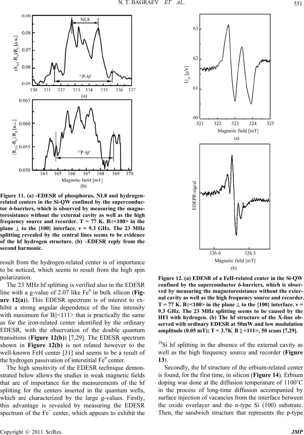 N. T. BAGRAEV ET AL. 551 Figure 11. (a) -EDESR of phosphorus, NL8 and hydrogen- related centers in the Si-QW confined by the superconduc- tor δ-barriers, which is observed by measuring the magne- toresistance without the external cavity as well as the high frequency source and recorder. T = 77 K. B׀׀<100> in the plane to the {100} interface. ν = 9.3 GHz. The 23 MHz splitting revealed by the central lines seems to be evidence of the hf hydrogen structure. (b) –EDESR reply from the second harmonic. result from the hydrogen-related center is of importance to be noticed, which seems to result from the high spin polarization. The 23 MHz hf splitting is verified also in the EDESR line with a g-value of 2.07 like Fe0 in bulk silicon (Fig- ure 12(a)). This EDESR spectrum is of interest to ex- hibit a strong angular dependence of the line intensity with maximum for B<111> that is practically the same as for the iron-related center identified by the ordinary EDESR, with the observation of the double quantum transitions (Figure 12(b)) [7,29]. The EDESR spectrum shown in Figure 12(b) is not related however to the well-known FeH center [31] and seems to be a result of the hydrogen passivation of interstitial Fe0 center. The high sensitivity of the EDESR technique demon- strated below allows the studies in weak magnetic fields that are of importance for the measurements of the hf splitting for the centers inserted in the quantum wells, which are characterized by the large g-values. Firstly, this advantage is revealed by measuring the EDESR spectrum of the Fe+ center, which appears to exhibit the Figure 12. (a) EDESR of a FeH-related center in the Si-QW confined by the superconductor δ-barriers, which is obser- ved by measuring the magnetoresistance without the exter- nal cavity as well as the high frequency source and recorder. T = 77 K. B׀׀<100> in the plane to the {100} interface. ν = 9.3 GHz. The 23 MHz splitting seems to be caused by the HFI with hydrogen. (b) The hf structure of the X-line ob- served with ordinary EDESR at 50mW and low modulation amplitude (0.05 mT); T = 3.7K. B || <111>, 50 scans [7,29]. 29Si hf splitting in the absence of the external cavity as well as the high frequency source and recorder (Figure 13). Secondly, the hf structure of the erbium-related center is found, for the first time, in silicon (Figure 14). Erbium doping was done at the diffusion temperature of 1100˚C in the process of long-time diffusion accompanied by surface injection of vacancies from the interface between the oxide overlayer and the n-type Si (100) substrate. Then, the sandwich structure that represents the p-type Copyright © 2011 SciRes. JMP 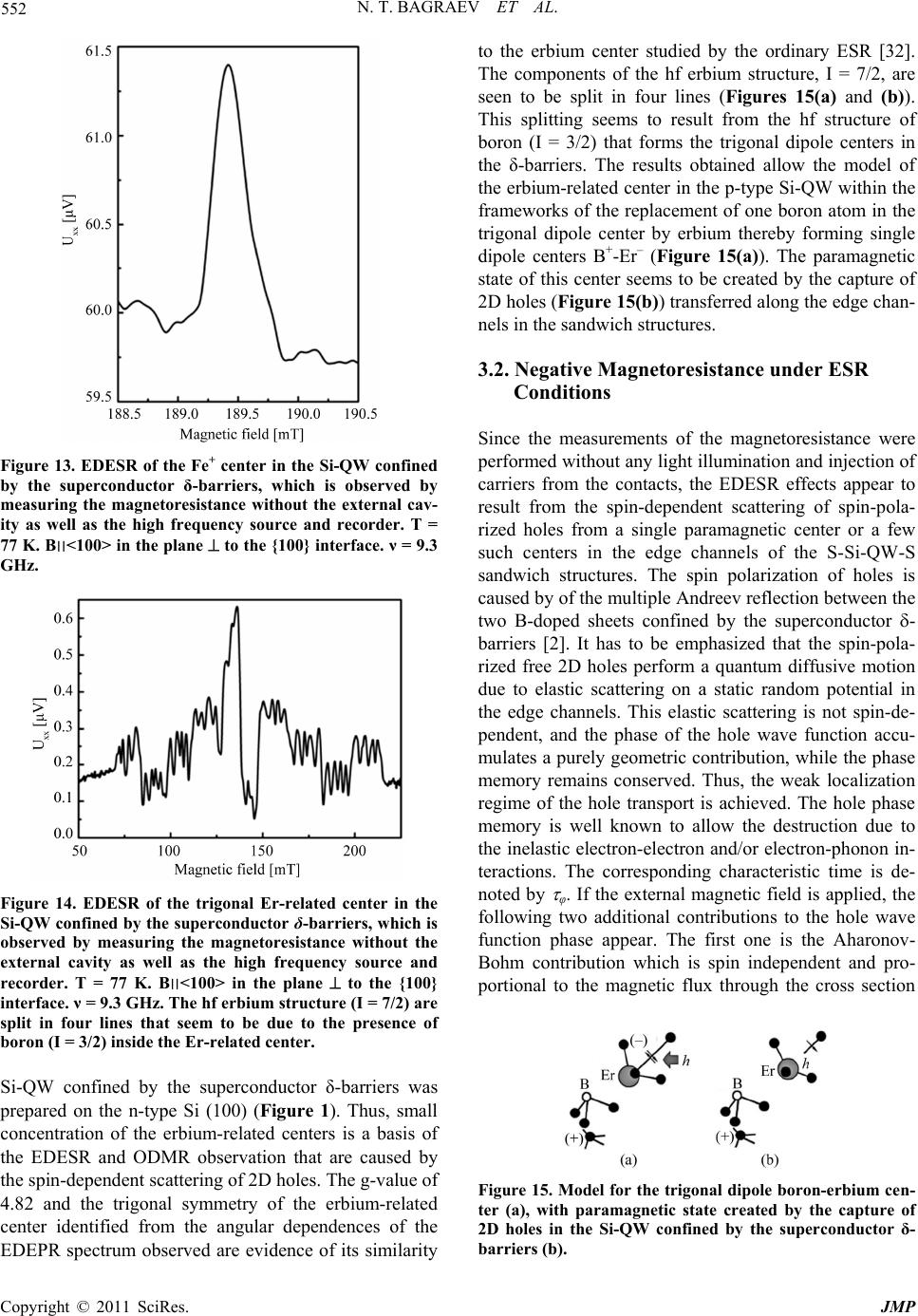 552 N. T. BAGRAEV ET AL. Figure 13. EDESR of the Fe+ center in the Si-QW confined by the superconductor δ-barriers, which is observed by measuring the magnetoresistance without the external cav- ity as well as the high frequency source and recorder. T = 77 K. B׀׀<100> in the plane to the {100} interface. ν = 9.3 GHz. Figure 14. EDESR of the trigonal Er-related center in the Si-QW confined by the superconductor δ-barriers, which is observed by measuring the magnetoresistance without the external cavity as well as the high frequency source and recorder. T = 77 K. B׀׀<100> in the plane to the {100} interface. ν = 9.3 GHz. The hf erbium structure (I = 7/2) are split in four lines that seem to be due to the presence of boron (I = 3/2) inside the Er-related center. Si-QW confined by the superconductor δ-barriers was prepared on the n-type Si (100) (Figure 1). Thus, small concentration of the erbium-related centers is a basis of the EDESR and ODMR observation that are caused by the spin-dependent scattering of 2D holes. The g-value of 4.82 and the trigonal symmetry of the erbium-related center identified from the angular dependences of the EDEPR spectrum observed are evidence of its similarity to the erbium center studied by the ordinary ESR [32]. The components of the hf erbium structure, I = 7/2, are seen to be split in four lines (Figures 15(a) and (b)). This splitting seems to result from the hf structure of boron (I = 3/2) that forms the trigonal dipole centers in the δ-barriers. The results obtained allow the model of the erbium-related center in the p-type Si-QW within the frameworks of the replacement of one boron atom in the trigonal dipole center by erbium thereby forming single dipole centers B+-Er– (Figure 15(a)). The paramagnetic state of this center seems to be created by the capture of 2D holes (Figure 15(b)) transferred along the edge chan- nels in the sandwich structures. 3.2. Negative Magnetoresistance under ESR Conditions Since the measurements of the magnetoresistance were performed without any light illumination and injection of carriers from the contacts, the EDESR effects appear to result from the spin-dependent scattering of spin-pola- rized holes from a single paramagnetic center or a few such centers in the edge channels of the S-Si-QW-S sandwich structures. The spin polarization of holes is caused by of the multiple Andreev reflection between the two B-doped sheets confined by the superconductor - barriers [2]. It has to be emphasized that the spin-pola- rized free 2D holes perform a quantum diffusive motion due to elastic scattering on a static random potential in the edge channels. This elastic scattering is not spin-de- pendent, and the phase of the hole wave function accu- mulates a purely geometric contribution, while the phase memory remains conserved. Thus, the weak localization regime of the hole transport is achieved. The hole phase memory is well known to allow the destruction due to the inelastic electron-electron and/or electron-phonon in- teractions. The corresponding characteristic time is de- noted by φ. If the external magnetic field is applied, the following two additional contributions to the hole wave function phase appear. The first one is the Aharonov- Bohm contribution which is spin independent and pro- portional to the magnetic flux through the cross section Figure 15. Model for the trigonal dipole boron-erbium cen- ter (a), with paramagnetic state created by the capture of 2D holes in the Si-QW confined by the superconductor δ- barriers (b). Copyright © 2011 SciRes. JMP 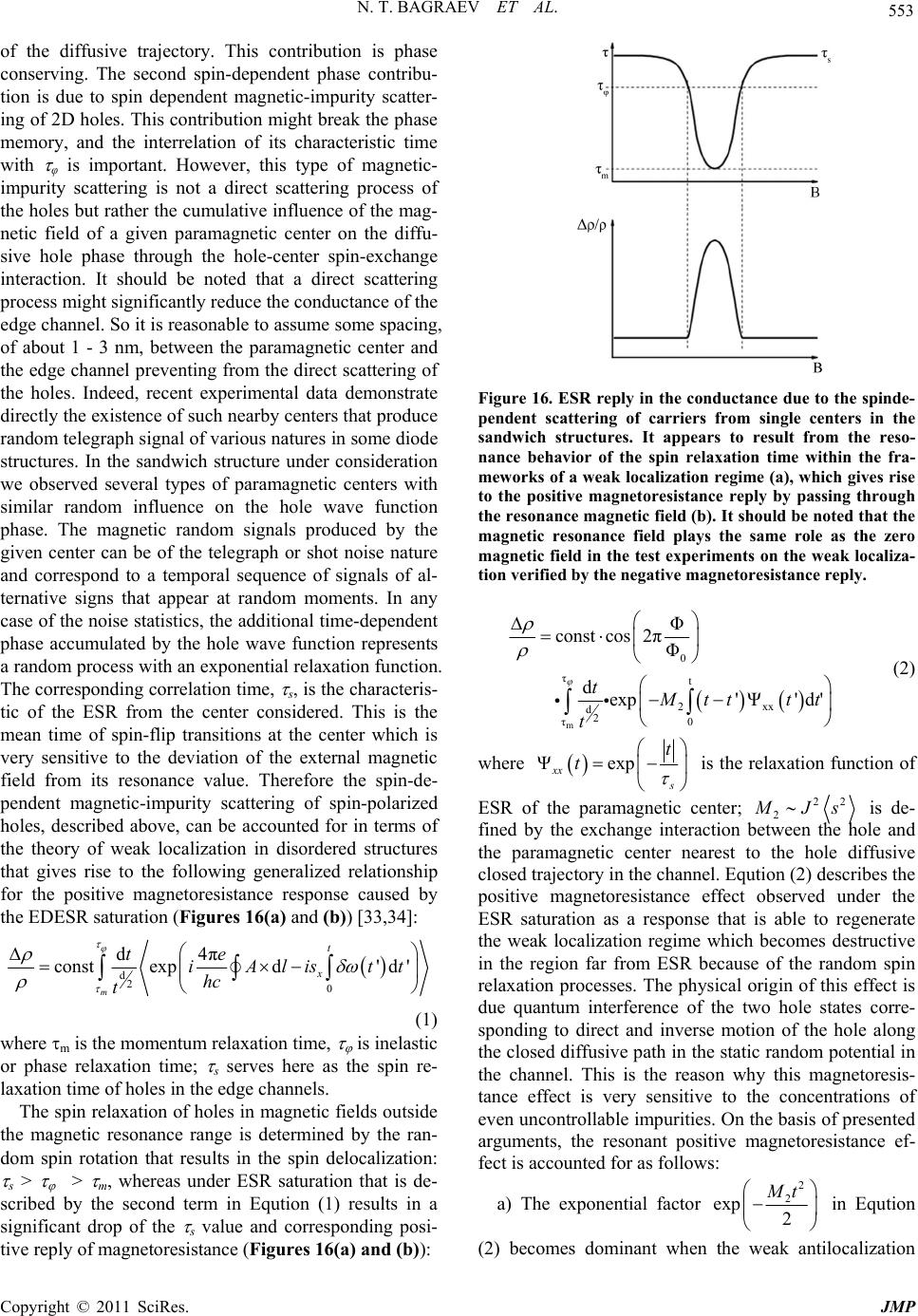 N. T. BAGRAEV ET AL. 553 of the diffusive trajectory. This contribution is phase conserving. The second spin-dependent phase contribu- tion is due to spin dependent magnetic-impurity scatter- ing of 2D holes. This contribution might break the phase memory, and the interrelation of its characteristic time with φ is important. However, this type of magnetic- impurity scattering is not a direct scattering process of the holes but rather the cumulative influence of the mag- netic field of a given paramagnetic center on the diffu- sive hole phase through the hole-center spin-exchange interaction. It should be noted that a direct scattering process might significantly reduce the conductance of the edge channel. So it is reasonable to assume some spacing, of about 1 - 3 nm, between the paramagnetic center and the edge channel preventing from the direct scattering of the holes. Indeed, recent experimental data demonstrate directly the existence of such nearby centers that produce random telegraph signal of various natures in some diode structures. In the sandwich structure under consideration we observed several types of paramagnetic centers with similar random influence on the hole wave function phase. The magnetic random signals produced by the given center can be of the telegraph or shot noise nature and correspond to a temporal sequence of signals of al- ternative signs that appear at random moments. In any case of the noise statistics, the additional time-dependent phase accumulated by the hole wave function represents a random process with an exponential relaxation function. The corresponding correlation time, s, is the characteris- tic of the ESR from the center considered. This is the mean time of spin-flip transitions at the center which is very sensitive to the deviation of the external magnetic field from its resonance value. Therefore the spin-de- pendent magnetic-impurity scattering of spin-polarized holes, described above, can be accounted for in terms of the theory of weak localization in disordered structures that gives rise to the following generalized relationship for the positive magnetoresistance response caused by the EDESR saturation (Figures 16(a) and (b)) [33,34]: d20 d4π constexpd' d ' m t x te iAlistt hc t (1) where m is the momentum relaxation time, is inelastic or phase relaxation time; s serves here as the spin re- laxation time of holes in the edge channels. The spin relaxation of holes in magnetic fields outside the magnetic resonance range is determined by the ran- dom spin rotation that results in the spin delocalization: s > > m, whereas under ESR saturation that is de- scribed by the second term in Eqution (1) results in a significant drop of the s value and corresponding posi- tive reply of magnetoresistance (Figures 16(a) and (b)): Figure 16. ESR reply in the conductance due to the spinde- pendent scattering of carriers from single centers in the sandwich structures. It appears to result from the reso- nance behavior of the spin relaxation time within the fra- meworks of a weak localization regime (a), which gives rise to the positive magnetoresistance reply by passing through the resonance magnetic field (b). It should be noted that the magnetic resonance field plays the same role as the zero magnetic field in the test experiments on the weak localiza- tion verified by the negative magnetoresistance reply. m 0 τt 2xx d2 τ0 Φ const cos2π Φ d exp'Ψ'd' t ttt t t (2) where Ψexp xx t t is the relaxation function of ESR of the paramagnetic center; 22 2 Js is de- fined by the exchange interaction between the hole and the paramagnetic center nearest to the hole diffusive closed trajectory in the channel. Eqution (2) describes the positive magnetoresistance effect observed under the ESR saturation as a response that is able to regenerate the weak localization regime which becomes destructive in the region far from ESR because of the random spin relaxation processes. The physical origin of this effect is due quantum interference of the two hole states corre- sponding to direct and inverse motion of the hole along the closed diffusive path in the static random potential in the channel. This is the reason why this magnetoresis- tance effect is very sensitive to the concentrations of even uncontrollable impurities. On the basis of presented arguments, the resonant positive magnetoresistance ef- fect is accounted for as follows: a) The exponential factor 2 2 exp 2 t in Eqution (2) becomes dominant when the weak antilocalization Copyright © 2011 SciRes. JMP 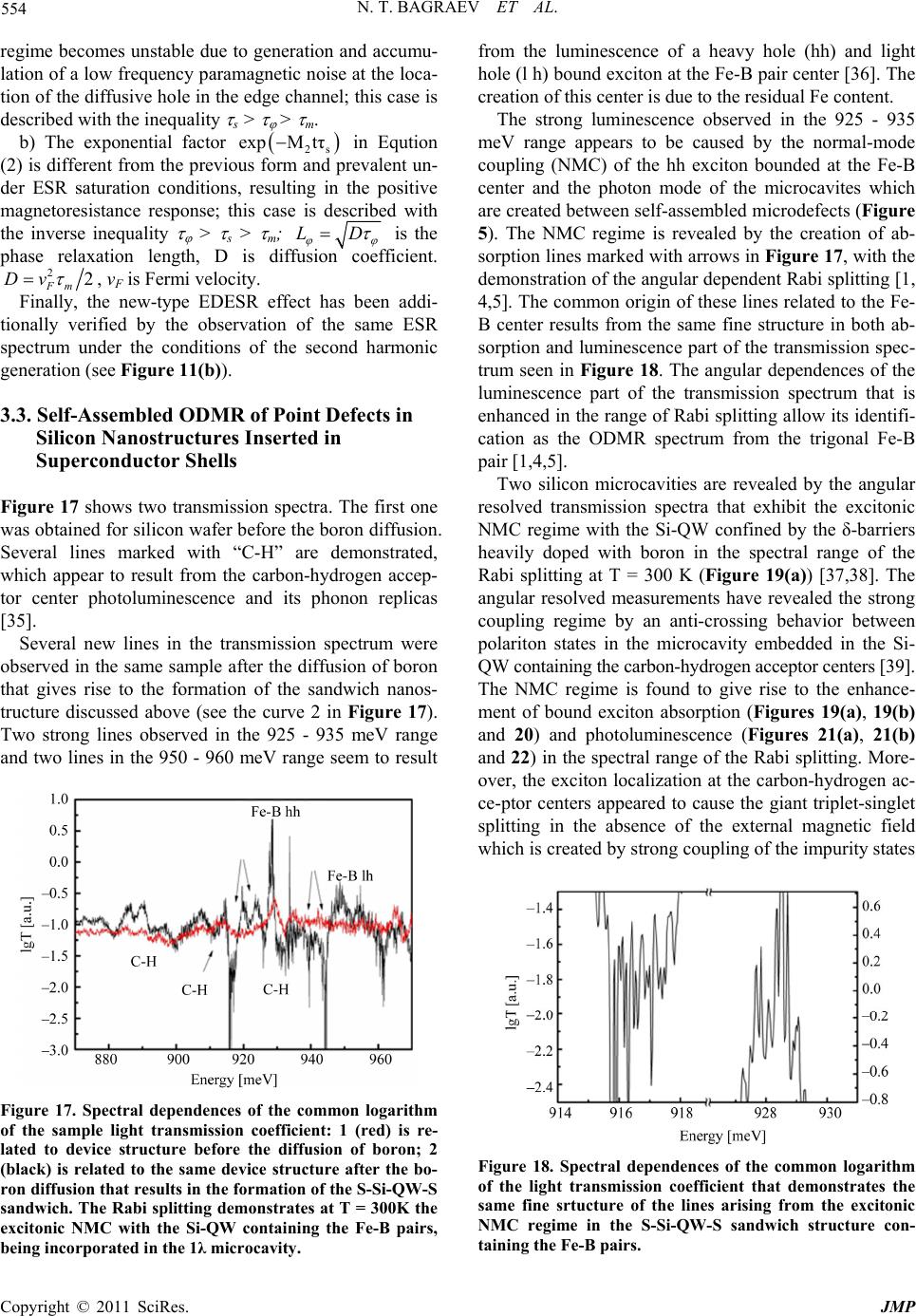 N. T. BAGRAEV ET AL. 554 regime becomes unstable due to generation and accumu- lation of a low frequency paramagnetic noise at the loca- tion of the diffusive hole in the edge channel; this case is described with the inequality s > > m. b) The exponential factor in Eqution (2) is different from the previous form and prevalent un- der ESR saturation conditions, resulting in the positive magnetoresistance response; this case is described with the inverse inequality > s > m; 2s expM tτ LD is the phase relaxation length, D is diffusion coefficient. 22 Fm Dv , vF is Fermi velocity. Finally, the new-type EDESR effect has been addi- tionally verified by the observation of the same ESR spectrum under the conditions of the second harmonic generation (see Figure 11(b)). 3.3. Self-Assembled ODMR of Point Defects in Silicon Nanostructures Inserted in Superconductor Shells Figure 17 shows two transmission spectra. The first one was obtained for silicon wafer before the boron diffusion. Several lines marked with “C-H” are demonstrated, which appear to result from the carbon-hydrogen accep- tor center photoluminescence and its phonon replicas [35]. Several new lines in the transmission spectrum were observed in the same sample after the diffusion of boron that gives rise to the formation of the sandwich nanos- tructure discussed above (see the curve 2 in Figure 17). Two strong lines observed in the 925 - 935 meV range and two lines in the 950 - 960 meV range seem to result Figure 17. Spectral dependences of the common logarithm of the sample light transmission coefficient: 1 (red) is re- lated to device structure before the diffusion of boron; 2 (black) is related to the same device structure after the bo- ron diffusion that results in the formation of the S-Si-QW-S sandwich. The Rabi splitting demonstrates at T = 300K the excitonic NMC with the Si-QW containing the Fe-B pairs, being incorporated in the 1λ microcavity. from the luminescence of a heavy hole (hh) and light hole (l h) bound exciton at the Fe-B pair center [36]. The creation of this center is due to the residual Fe content. The strong luminescence observed in the 925 - 935 meV range appears to be caused by the normal-mode coupling (NMC) of the hh exciton bounded at the Fe-B center and the photon mode of the microcavites which are created between self-assembled microdefects (Figure 5). The NMC regime is revealed by the creation of ab- sorption lines marked with arrows in Figure 17, with the demonstration of the angular dependent Rabi splitting [1, 4,5]. The common origin of these lines related to the Fe- B center results from the same fine structure in both ab- sorption and luminescence part of the transmission spec- trum seen in Figure 18. The angular dependences of the luminescence part of the transmission spectrum that is enhanced in the range of Rabi splitting allow its identifi- cation as the ODMR spectrum from the trigonal Fe-B pair [1,4,5]. Two silicon microcavities are revealed by the angular resolved transmission spectra that exhibit the excitonic NMC regime with the Si-QW confined by the δ-barriers heavily doped with boron in the spectral range of the Rabi splitting at T = 300 K (Figure 19(a)) [37,38]. The angular resolved measurements have revealed the strong coupling regime by an anti-crossing behavior between polariton states in the microcavity embedded in the Si- QW containing the carbon-hydrogen acceptor centers [39]. The NMC regime is found to give rise to the enhance- ment of bound exciton absorption (Figures 19(a), 19(b) and 20) and photoluminescence (Figures 21(a), 21(b) and 22) in the spectral range of the Rabi splitting. More- over, the exciton localization at the carbon-hydrogen ac- ce-ptor centers appeared to cause the giant triplet-singlet splitting in the absence of the external magnetic field which is created by strong coupling of the impurity states Figure 18. Spectral dependences of the common logarithm of the light transmission coefficient that demonstrates the same fine srtucture of the lines arising from the excitonic NMC regime in the S-Si-QW-S sandwich structure con- taining the Fe-B pairs. Copyright © 2011 SciRes. JMP 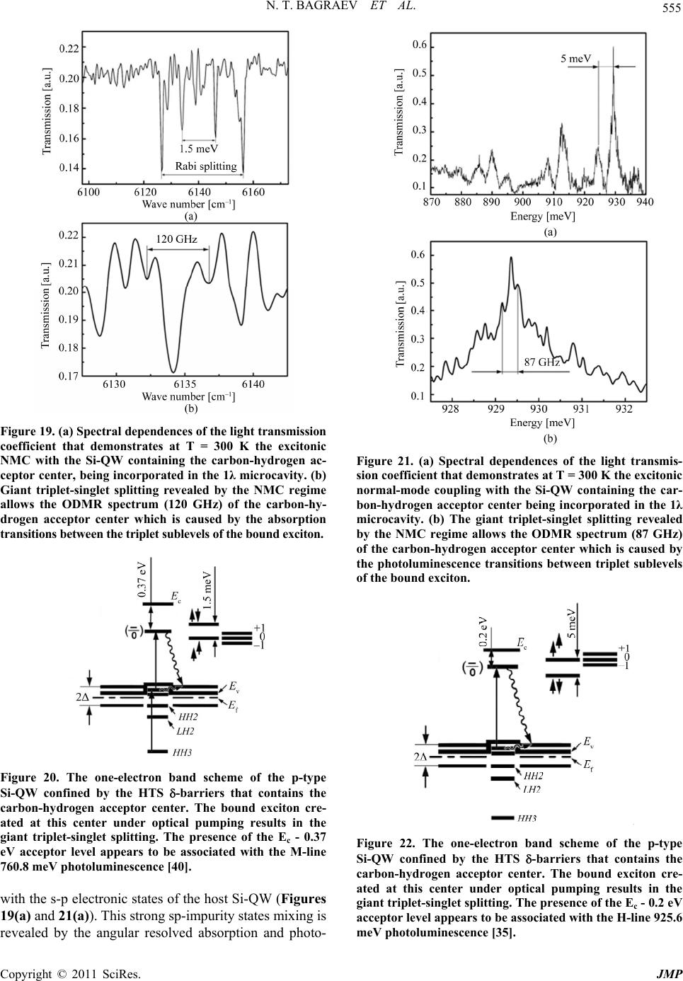 N. T. BAGRAEV ET AL. 555 Figure 19. (a) Spectral dependences of the light transmission coefficient that demonstrates at T = 300 K the excitonic NMC with the Si-QW containing the carbon-hydrogen ac- ceptor center, being incorporated in the 1λ microcavity. (b) Giant triplet-singlet splitting revealed by the NMC regime allows the ODMR spectrum (120 GHz) of the carbon-hy- drogen acceptor center which is caused by the absorption transitions between the triplet sublevels of the bound exciton. Figure 20. The one-electron band scheme of the p-type Si-QW confined by the HTS -barriers that contains the carbon-hydrogen acceptor center. The bound exciton cre- ated at this center under optical pumping results in the giant triplet-singlet splitting. The presence of the Ec - 0.37 eV acceptor level appears to be associated with the M-line 760.8 meV photoluminescence [40]. with the s-p electronic states of the host Si-QW (Figures 19(a) and 21(a)). This strong sp-impurity states mixing is revealed by the angular resolved absorption and photo- Figure 21. (a) Spectral dependences of the light transmis- sion coefficient that demonstrates at T = 300 K the excitonic normal-mode coupling with the Si-QW containing the car- bon-hydrogen acceptor center being incorporated in the 1λ microcavity. (b) The giant triplet-singlet splitting revealed by the NMC regime allows the ODMR spectrum (87 GHz) of the carbon-hydrogen acceptor center which is caused by the photoluminescence transitions between triplet sublevels of the bound exciton. Figure 22. The one-electron band scheme of the p-type Si-QW confined by the HTS -barriers that contains the carbon-hydrogen acceptor center. The bound exciton cre- ated at this center under optical pumping results in the giant triplet-singlet splitting. The presence of the Ec - 0.2 eV acceptor level appears to be associated with the H-line 925.6 meV photoluminescence [35]. Copyright © 2011 SciRes. JMP  556 N. T. BAGRAEV ET AL. luminescence that seem to reveal the ODMR spectra in zero magnetic field under the NMC conditions (Figures 19(b) and 21(b)), because the EPR frequency is able to be selected from the THz range generated by the δ-barriers confining the Si-QW being in self-agreement with the splitting of the triplet sublevels in the exchange field induced by the bound exciton (Figures 20 and 22) [1,4, 5]. Two different carbon-hydrogen acceptor centers, Cs- Ci-H [39], have been identified by measuring the ODMR spectra. The first center that is sensitive to the frequency value of 120 GHz seems to be associated with the pres- ence of the Ec - 0.37 eV acceptor level which appears to give rise to the M-line 760.8 meV photoluminescence (Figures 19(a) and 20) [40]. The bound exciton absorp- tion is predominant in the ODMR spectrum, because the energy of optical transition from the HH1 subband of 2D holes to the Ec - 0.37 eV acceptor level appears to be in resonance with the HH3 - HH1 optical transition in the Si-QW. It should be noted that the double quantum tran- sitions seem to be exhibited in the ODMR spectrum (Figure 19(a)). The second center that is sensitive to the frequency value of 87 GHz seems to be associated with the presence of the Ec - 0.2 eV acceptor level which ap- pears to give rise to the H-line 925.6 meV photolumi- nescence (Figures 19(a), 19(b) and (20)) [35]. The pho- non replica are observed in the photoluminescence spec- trum that reveals also the giant triplet-singlet splitting, 5 meV. The multi-quantum transitions are seen to contri- bute to the ODMR spectrum (Figure 21(b)). Finally, the frequency values of 120 GHz and 87 GHz revealed by the modulation of the transmission spectra correlate with the splitting of the triplet sublevels in the exchange field induced by the bound exciton which appears to result from the ODMR spectra. 4. Conclusions The new electrically- and optically-detected ESR (EDESR and ODMR) technique, which allows the studies without using an external cavity and a high frequency source and recorder, has been demonstrated by measuring respec- tively the only magnetoresistance and transmission spec- tra. Using this new EDESR technique, the ESR spec- trometer has been suggested to be replaced by the sand- wich structure that represents the ultra-narrow silicon quantum well confined by the superconductor δ-barriers. These δ-barriers appeared to be the sources of the GHz and THz emission that can be enhanced by varying the dimensions of the sandwich structure which is able to form the internal cavity. This new EDESR technique has been applied to the studies of the phosphorus, iron-, hy- drogen- and erbium-related centers embedded in the ul- tra-narrow p-type silicon quantum well that was a basis of the sandwich structure. The hf erbium structure signal has been found, for the first time, for the erbium-related centers in silicon. The excitonic normal-mode coupling (NMC) with the single p-type Si-QW incorporated in the 1 silicon mi- crocavity on the n-type Si (100) wafer has been identi- fied at T = 300 K in the studies of the transmission spec- tra which have revealed the ODMR of the trigonal Fe-B pairs and the single carbon-hydrogen acceptor center in the absence of the external magnetic field, the external cavity and the hf source. It is pointed out that the reso- nant positive magnetoresistance data can be interpreted in terms of the interference transition within the frame- works of the diffusive transport of free holes in the weak antilocalization regime due to the spin relaxation pro- cesses as the external magnetic field value goes through the defect ESR resonance field corresponding to a para- magnetic center. 5. Acknowledgements The work was supported by the programme of funda- mental studies of the Presidium of the Russian Academy of Sciences “Quantum Physics of Condensed Matter” (grant 9.12); programme of the Swiss National Science Foundation (grant IZ73Z0_127945/1); the Federal Tar- geted Programme on Research and Development in Pri- ority Areas for the Russian Science and Technology Complex in 2007 - 2012 (contract no. 02.514.11.4074), the SEVENTH FRAMEWORK PROGRAMME Marie Curie Actions PIRSES-GA-2009-246784 project SPIN- MET. 6. References [1] N. T. Bagraev, W. Gehlhoff, L. E. Klyachkin, A. M. Malyarenko, V. A. Mashkov, V. V. Romanov and T. N. She-lykh, “ODMR of Impurity Centers Embedded in Sili- con Microcavities,” Physica E, Vol. 40, No. 5, 2008, pp. 1627-1629. doi:10.1016/j.physe.2007.10.005 [2] N. T. Bagraev, W. Gehlhoff, L. E. Klyachkin, A. A. Kudryavtsev, A. M. Malyarenko, G. A. Oganesyan, D. S. Poloskin and V. V. Romanov, “Spin-Dependent Trans- port of Holes in Silicon Quantum Wells Confined by Su- perconductor Barriers,” Physica C, Vol. 468, No. 7-10, 2008, pp. 840-843. doi:10.1016/j.physc.2007.11.060 [3] N. T. Bagraev, N. G. Galkin, W. Gehlhoff, L. E. Klyach- kin and A. M. Malyarenko, “Phase and Amplitude Re- sponse of the ‘0.7 feature’ Caused by Holes in Silicon One-dimensional Wires and Rings,” Journal of Physics: Condensed Matter, Vol. 20, No. 16, 2008, Article ID 164202- 1-10.doi:10.1088/0953-8984/20/16/164202 [4] N. T. Bagraev, A. D. Bouravleuv, W. Gehlhoff, L. E. Kly-achkin, A. M. Malyarenko and V. V. Romanov, Copyright © 2011 SciRes. JMP  N. T. BAGRAEV ET AL. 557 “Electron-Dipole Resonance of Impurity Centres Em- bedded in Silicon Microcavities,” Physica B, Vol. 340-342, 2003, pp. 1078-1081. doi:10.1016/j.physb.2003.09.184 [5] N. T. Bagraev, A. D. Bouravleuv, W. Gehlhoff, L. E. Kly-achkin, A. M. Malyarenko and V. V. Romanov, “Electron-Dipole Resonance of Impurity Centres Em- bedded in Silicon Microcavities,” Physica Status Solidi (c), Vol. 2, No. 2, 2005, pp. 783-786. doi:10.1002/pssc.200460353 [6] J. P. Kotthaus and R. Ranvaud, “Cyclotron Resonance of Holes in Surface Space Charge Layers on Si,” Physical Review B, Vol. 15, No. 12, 1977, pp. 5758-5761. doi:10.1103/PhysRevB.15.5758 [7] N. T. Bagraev, W. Gehlhoff and L. E. Klyachkin, “Cy- clotron Resonance in Heavily Doped Silicon Quantum Wells,” Solid State Phenomena, Vol. 47-48, 1995, pp. 589-594. [8] B.-X. Li, P.-L. Cao and D.-L. Que, “Distorted IcoSahe- dral Cage Structure of Si60 Clusters,” Physical Review B, Vol. 61, No. 3, 2000, pp. 1685-1687. doi:10.1103/PhysRevB.61.1685 [9] N. T. BagraeV, A. D. Bouravleuv, L. E. Klyachkin, A. M. Malyarenko, W. Gehlhoff, Yu. I. Romanov and S. A. Rykov, “Local Tunneling Spectroscopy of Silicon Nanos- tructures,” Semiconductors, Vol. 39, No. 6, 2005, pp. 716-728. [10] N. T. Bagraev, A. D. Bouravleuv, L. E. Klyachkin, A. M. Malyarenko, W. Gehlhoff, V. K. Ivanov and I. A. She- lykh, “Quantized Conductance in Silicon Quantum Wires,” Semiconductors, Vol. 36, No. 4, 2002, pp. 439-460. doi:10.1134/1.1469195 [11] A. Slaoui, E. Fogarassy, J. C. Muller and P. Siffert, “Study of Some Optical and Electrical Properties of Heavily Doped Silicon Layers,” Journal de Physique Colloques, Vol. 44, No. C5 44, 1983, pp. 65-71. [12] N. T. Bagraev, A. D. Bouravleuv, L. E. Klyachkin, A. M. Malyarenko and S. A. Rykov, “Self-Ordered Microcavi- ties Embedded in Ultra-shallow Silicon p-n Junctions,” Semiconductors, Vol. 34, No. 6, 2000, pp. 700-711. doi:10.1134/1.1188058 [13] R. Laiho, M. M. Afanasjev, M. P. Vlasenko and L. S. Vlasenko, “Electron Exchange Interaction in S = 1 De- fects Observed by Level Crossing Spin Dependent Mi- crowave Photo-Conductivity in Irradiated Silicon,” Phy- sical Review Letters, Vol. 80, No. 7, 1998, pp. 1489-1492. doi:10.1134/1.1188058 [14] N. T. Bagraev, N. G. Galkin, W. Gehlhoff, L. E. Klyach- kin, A. M. Malyarenko and I. A. Shelykh, “Spin Interfer- ence in Silicon One-Dimensional Rings,” Journal of Physsical: Condensed. Matter, Vol. 18, No. 45, 2006, pp. L567-L573. doi:10.1088/0953-8984/18/45/L01 [15] N. T. Bagraev, N. G. Galkin, W. Gehlhoff, L. E. Klyach- kin, A. M. Malyarenko and I. A. Shelykh, “Spin Interfer- ence in Silicon One-Dimensional Rings,” Physica E, Vol. 40, No. 5, 2008, pp. 1338-1340. doi:10.1016/j.physe.2007.08.079 [16] N. T. Bagraev, A. D. Bouravleuv, W. Gehlhoff, L. E. Kly-achkin, A. M. Malyarenko and V. V. Romanov, “Er-bium-related Centres Embedded in Silicon Micro- cavities,” Physica B, Vol. 340-342, 2003, pp. 1074-1077. doi:10.1016/j.physe.2007.08.079 [17] A. Alexandrov and J. Ranninger, “Bipolaronic Super- conductivity,” Physical Review B, Vol. 24, No 3, 1981, pp. 1164-1169. doi:10.1103/PhysRevB.24.1164 [18] A. S. Alexandrov and N. F. Mott, “Bipolarons,” Reports on Progress in Physics, Vol. 57, No. 12, December 1994, pp. 1197-1288. doi:10.1088/0034-4885/57/12/001 [19] V. L. Ginzburg, “On Surface Superconductivity,” Physics Letters, Vol. 13, No. 2, 1964, pp. 101-104. doi:10.1016/0031-9163(64)90672-9 [20] A. I. Larkin and Yu. N. Ovchinnikov, “Nonuniform State of Superconductors,” Soviet Physics-JETP, Vol. 20, No. 3, 1965, pp. 762-770. [21] P. Fulde and R. A. Ferrell, “Superconductivity in a Strong Spin-Exchange Field,” Physical Review, Vol. 135, No. 3A, 1964, pp. A550-A563. doi:10.1103/PhysRev.135.A550 [22] W. A. Little, “Higher Temperatures: Theoretical Mod- els,” Physica, Vol. 55, 1971, pp. 50-54. doi:10.1016/0031-8914(71)90240-0 [23] N. T. Bagraev and V. A. Mashkov, “Tunneling Nega- tive-U Centers and Photo-Induced Reactions in Solids,” Solid State Communications, Vol. 51, No. 7, 1984, pp. 515-521. doi:10.1016/0038-1098(84)91024-X [24] N. T. Bagraev and V. A. Mashkov, “A Mechanism for Two-Electron Capture at Deep Level Defects in Semi- conductors, Solid State Communications,” Solid State Communications, Vol. 65, No. 12, 1988, pp. 1111-1117. doi:10.1016/0038-1098(88)90904-0 [25] M. Tinkham, “Introduction to Superconductivity,” Dover, New York, 1996. [26] I. A. Shelykh, M. A. Kulov, N. G. Galkin and N. T. Ba- graev, “Spin-Dependent Transport Caused by the Local Magnetic Moments Inserted in the Aharonov–Bohm rings,” Journal of Physics: Condensed Matter, Vol. 19, No. 24, 2007, pp. 246207-1-14. doi:10.1088/0953-8984/19/24/246207 [27] M. Rosenau Da Costa, I. A. Shelykh and N. T. Bagraev, “Fractional Quantization of Ballistic Conductance in One-Dimensional Hole Systems,” Physical Review B, Vol. 76, No. 20, 2007, pp. 201302R-1-4. [28] H. H. P. Th. Bekman, T. Gregorkiewicz and C. A. J. Am- merlaan, “Si-NL10: Paramagnetic Acceptor State of the Silicon Thermal Donor,” Physical Review Letters, Vol. 61, No. 2, 1988, pp. 227-230. doi:10.1103/PhysRevLett.61.227 [29] W. Gehlhoff, K. Irmscher, N. T. Bagraev, L. E. Klyach- kin and A. M. Malyarenko, “Shallow Centers in Heavily Doped Silicon Quantum Wells,” In: C. A. J. Ammerlaan and B. Pajot, Eds., Shallow Level Centres in Semicon- ductors, World Scientific, Singapore, 1997, pp. 227-232. [30] B. N. Mukashev, Kh. A. Abdullin and Yu. V. Gorelkin- skii, “Metastable and Bistable Defects in Silicon,” Phys- ics-Uspekhi, Vol. 43, No. 2, 2000, pp. 139-150. Copyright © 2011 SciRes. JMP  N. T. BAGRAEV ET AL. Copyright © 2011 SciRes. JMP 558 doi:10.1070/PU2000v043n02ABEH000649 [31] C. A. J. Ammerlaan and P. T. Huy, “Characterisation of Hydrogen and Hydrogen-Related Centres in Crystalline Silicon by Magnetic-Resonance Spectroscopy,” Solid State Phenomena, Vol. 85-86, 2002, pp. 353-370. doi:10.4028/www.scientific.net/SSP.85-86.353 [32] J. D. Carey, R. C. Barklie and J. F. Donegan, “Electron Paramagnetic Resonance and Photoluminescence Study of Er-Impurity Complexes in Si,” Physical Review B, Vol. 59, No. 4, 1999, pp. 2773-2782. doi:10.1103/PhysRevB.59.2773 [33] R. Kubo and K. Tomita, “A General Theory of Magnetic Resonance Absorption,” Journal of the Physical Society of Japan, Vol. 9, No. 6, 1954, pp. 888-919. doi:10.1143/JPSJ.9.888 [34] R. Kubo, “Note on the Stochastic Theory of Resonance Absorption,” Journal of the Physical Society of Japan, Vol. 9, No. 6, 1954, pp. 935-944. doi:10.1143/JPSJ.9.935 [35] E. C. Lightowlers and A. N. Safonov, “Photoluminescence Vibrational Spectroscopy of Defects Containing the Light Impurities Carbon and Oxygen in Silicon,” Materials Sci- ence Forum, Vol. 258-263, 1997, pp. 617-622. [36] S. Ghatnekar-Nilsson, M. Kleverman, P. Emanuelsson and H.G. Grimmeiss, “Identification of the Iron-Boron line Spectrum in Silicon,” Semiconductor Science and Technology, Vol. 8, No. 10, 1993, pp. 1857-1861. doi:10.1088/0268-1242/8/10/012 [37] C. Weisbuch, M. Nishioka, A. Ishikawa and Y. Arakawa, “Observation of the Coupled Exciton-Photon Mode Split- ting in a Semiconductor Quantum Microcavity,” Physical Review Letters, Vol. 69, No. 23, 1992, pp. 3314-3317. doi:10.1103/PhysRevLett.69.3314 [38] G. Khitrova, H. M. Gibbs, F. Jahnke, M. Kira and S. W. Koch, “Nonlinear Optics of Normal-Mode-Coupling Semiconductor Microcavities,” Review of Modern Phys- ics, Vol. 71, No. 5, 1999, pp. 1591-1639. doi:10.1103/RevModPhys.71.1591 [39] A. Mainwood, “The Trapping of Hydrogen at Carbon Defects in Silicon,” Materials Science Forum, Vol. 258-263, 1997, pp. 253-258. [40] A. N. Safonov and E. C. Lightowlers, “The M-line (760.8 meV) Luminescence System Associated with the Car- bon-Hydrogen Acceptor Centre in Silicon,” Materials Science Forum, Vol. 258-263, 1997, pp. 259-264.
|