 Open Journal of Acoustics 2011. Vol.1, No.1, 1-8 Copyright © 2011 SciRes. DOI:10.4236/oja.2011.11001 Surface Wave Characteristics at the Interface of Welded Elastic Halfspaces J. N. Sharma1, K. K. Sharma2, Ashwani Kumar2 1Department of Mathematics, National Institute of Technology, Hamirpur, India; 2Department of Physics, National Institute of Technology,Hamirpur, India. Email: jns@nitham.ac.in, kks@nitham.ac.in, puri_nit@yahoo.com Received June 1st, 2011; revised June 20th, 2011; accepted June 25th, 2011. The present article concentrates on the propagation of generalized surface acoustic waves in a composite struc- ture consisting of piezoelectric and non-piezoelectric semiconductor media. The mathematical model of the problem is depicted by a set of partial differential equations of motion, Gauss equation in piezoelectric and elec- tron diffusion equation in semiconductor along with boundary conditions to be satisfied at the interface. The secular equation that governs the propagation of surface waves has been derived in compact form after obtaining the formal solution. The analytic expressions for displacements, stresses, piezoelectric potential and electron concentration during the surface wave propagation at the interface have also been obtained. The numerical solu- tion of the secular equation is carried out for the cadmium selenide and silicon composite by employing fixed point functional iteration numerical method along with irreducible Cardano method. The computer simulated results with the help of MATLAB software in respect of dispersion curves, attenuation coefficient, displace- ments, stresses, carrier concentration and piezoelectric potential are presented graphically. This work may be useful in surface acoustic wave ( S AW) devices and electronic industry . Keywords: Piezoelectrics, Life Time, Silicon, Dispersive Waves, Attenuation Introduction The piezoelectric effect in certain noncentro-symmetric crystalline materials was discovered by Curie and Curie (1880). Parmenter (1953) regarded the appearance of DC electric field along the direction of propagation of a acoustic wave in a me- dium containing mobile charges as acoustoelectric effect. Weinreich et al. (1959) termed acoustoelectric effect as wave particle drag phenomenon. Hutson and White (1962) found that the field produced along the traveling acoustic wave produces current and space charges which results in acoustic dispersion and loss. According to White (1962) an acoustic wave traveling in a piezoelectric semiconductor can be amplified or attenuated by the application of a DC electric field. Collins et al. (1968) found the strong interaction between the wave on the surface of piezoelectric crystal and the wave on the drifting carriers in a nearby semiconductor. Bluestein (1968) and Gulyaev (1969) studied surface acoustic waves in piezoelectric materials. Fis- chler (1970) proposed that acoustoelectric amplification can be better obtained in composite structure of semiconductor and piezoelectric materials. Dietz et al. (1988) explored that the acoustoelectric amplification of acoustic waves can also be achieved through composite of a piezoelectric dielectric and non-piezoelectric semiconductor. de Lorenzi and Tierten (1975), and Maugin and Dehar (1986) developed nonlinear theories for deformable semiconductors. Ingebrigtsen (1970) studied linear and non-linear attenuation of acoustic surface waves in a piezoelectric coated with a semi- conductor film. Tien (1968) presented the nonlinear theory of ultrasonic amplification and current saturation in piezoelectric semiconductors. Kagan (1997) investigated the surface wave propagation in a piezoelectric crystal underlying a two dimen- sional conducting layer. Jin et al. (2002) studied the Lamb wave propagation in a metallic semi-infinite medium covered with piezoelectric layer. Wang (2002) investigated wave propagation in the piezoelectric solid medium. Yang and Zhou (2005) investigated amplification of acoustic waves in piezo- electric semiconductor plates. Yang and Zhou (2005) also stud- ied the propagation and amplification of gap waves between a piezoelectric halfspace and a semiconductor film. Maruszewski (1989) considered the interactions between elastic, thermal and charge carrier’s fields in semiconductors and predicted the ex- istence of two kinds of waves namely, polarized and dispersive waves. Kleinert et al. (2005) studied the surface-acoustic-wave- induced space-charge waves in electron-hole systems. Sharma and Pal (2004) investigated the propagation of Lamb waves in homogeneous, transversely isotropic, piezothermoe- lastic plate. Sharma et al. (2005) studied the propagation cha- racteristics of Rayleigh waves in transversely isotropic pie- zothermoelastic mater i a ls . Th e p hase velocity profiles are found to be dispersive at small values of wave number and these be- come asymptotically linear at higher values of wave numbers. Sharma and Walia (2007) carried out further investigations on the propagation of Rayleigh waves in a homogeneous, trans- versely isotropic, piezothermoelastic semi-space. Sharma and Thakur (2006) studied the plane harmonic elasto-thermodiffu- sive waves in semiconductor materials. Sharma et al. (2007, 2009) also investigated the characteristics of elasto-thermodif- fusive wave propagation on semiconductor materials and ob- served that life time of charge carriers and thermal relaxation time affects the wave characteristics significantly at long wavelengths as compared to that at short wavelengths. Sharma et al. (2008) investigated the elasto-thermodiffusive surface 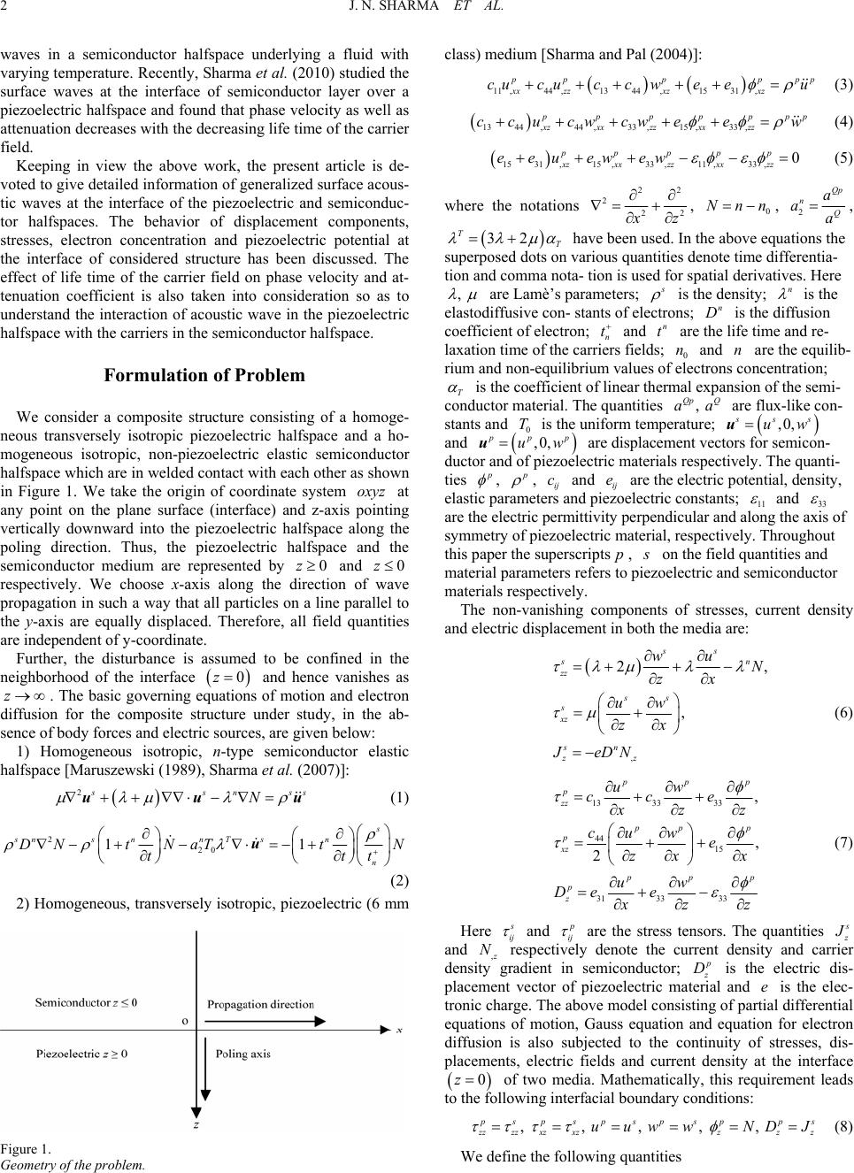 J. N. SHARMA ET AL. 2 waves in a semiconductor halfspace underlying a fluid with varying temperature. Recently, Sharma et al. (2010) studied the surface waves at the interface of semiconductor layer over a piezoelectric halfspace and found that phase velocity as well as attenuation de crea ses wit h the de cr easi ng life time of th e c arrie r field. Keeping in view the above work, the present article is de- voted to give detailed information of generalized surface acous- tic waves at the interface of the piezoelectric and semiconduc- tor halfspaces. The behavior of displacement components, stresses, electron concentration and piezoelectric potential at the interface of considered structure has been discussed. The effect of life time of the carrier field on phase velocity and at- tenuation coefficient is also taken into consideration so as to understand the interaction of acoustic wave in the piezoelectric halfspace with the carriers in the semiconductor halfspace. Formulation of Problem We consider a composite structure consisting of a homoge- neous transversely isotropic piezoelectric halfspace and a ho- mogeneous isotropic, non-piezoelectric elastic semiconductor halfspace which are in welded contact with each other as shown in Figure 1. We take the origin of coordinate system at any point on the plane surface (interface) and z-axis pointing vertically downward into the piezoelectric halfspace along the poling direction. Thus, the piezoelectric halfspace and the semiconductor medium are represented by and oxyz z 0z0 respectively. We choose x-axis along the direction of wave propagation in such a way that all particles on a line parallel to the y-axis are equally displaced. Therefore, all field quantities are independent o f y-coo r d i nate. Further, the disturbance is assumed to be confined in the neighborhood of the interface 0z and hence vanishes as . The basic governing equations of motion and electron diffusion for the composite structure under study, in the ab- sence of body forces and electric sources, are given below: z 1) Homogeneous isotropic, n-type semiconductor elastic halfspace [Maruszewski (1989), Sharma et al. (2007)]: 2 sn s N uus u (1) 220 11 s snsnn Tsn n DNt NaTtN tt u t (2) 2) Homogeneous, transversely isotropic, piezoelectric (6 mm Figure 1. Geometry of the problem. class) medium [Sharma and Pal (2004)]: 11 ,44 ,1344,1531, ppp xx zzxzxz cucuccweeu pp (3) 1344, 44, 33,15,33, ppppp xzxxzz xx zz ccu cwcweew p (4) 1531,15,33,11 ,33 ,0 pp ppp xzxxzz xxzz eeu ewew (5) where the notations 22 2 22 z , 0 nn , 2 Qp n Q a aa , 32 TT , have been used. In the above equations the superposed dots on various quantities denote time differentia- tion and comma nota- tion is used for spatial derivatives. Here are Lamè’s parameters; is the density; n is the elastodiffusive con- stants of electrons; is the diffusion coefficient of electron; n n D t and are the life time and re- laxation time of the carriers fields; 0 and are the equilib- rium and non-equilibrium values of electrons concentration; T n tnn is the coefficient of linear thermal expansion of the semi- conductor material. The quantities are flux-like con- stants and is the uniform temperature; , Q a Qp a 0 T ,0, ss uwu and ,0, p uup w are displacement vectors for semicon- ductor and of piezoelectric materials respectively. The quanti- ties , , ij and ij e are the electric potential, density, elastic parameters and piezoelectric constants; 11 c and 33 are the electric permittivity perpendicular and along the axis of symmetry of piezoelectric material, respectively. Throughout this paper the superscripts, p on the field quantities and material parameters refers to piezoelectric and semiconductor materials respectively. The non-vanishing components of stresses, current density and electric displacement in both the media are: , 2, , ss sn zz ss s xz sn zz wu zx uw zx JeDN (6) 13 3333 44 15 31 3333 , , 2 pp p zz pp p xz pp p z uw cce zz cu we zx x uw De e zz (7) Here ij and ij are the stress tensors. The quantities and , respectively denote the current density and carrier density gradient in semiconductor; D is the electric dis- placement vector of piezoelectric material and is the elec- tronic charge. The above model consisting of partial differential equations of motion, Gauss equation and equation for electron diffusion is also subjected to the continuity of stresses, dis- placements, electric fields and current density at the interface e 0z of two media. Mathematically, this requirement leads to the following interfacial boundary conditions: , , , , , spsp spspps zzzxzxzz z uuww NDJ z (8) We define the following quantities 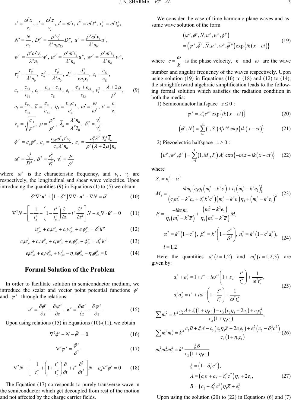 J. N. SHARMA ET AL. 3 ** 2 0033 0 00 1 000 , , , , , , , , , , , , , , nn nn ll ss ppss ll zz nn sss 0 spp pp ll nnn ps s ij ij pss z ijij z nn l xz l ztttttt vv Nv v NDDu u nne n vv wwuuw nnn Jc Jc nnenv v w 2 33 11 2 4413 4415 31 23 1 11 1133 15113311 23 2 33 3333 2 2 110 12 0 2 332 0 11 0 , 2 , , , , , , , , , , , , , 2 ls l pn l pn ps Tp snT pp ln pp n ns c cccee cce v cc e ec e ee cnv vTv ev aT cn c c v 0 22 22 2 , , lt t ns l n vv v Dv (9) where is the characteristic frequency, and l v, t are respectively, the longitudinal and shear wave velocities. Upon introducing the quantities (9) in Equations (1) to (5) we obtain v 22 2 1 s N uu s u (10) 2 2 2 110 nns n nn t NtN tttt u (11) 2 ,2,3,1,1 ppp xxzzxz xz ucucwe u p (12) 2 3,2, 1, 2,,1 pppp xzxxzzxx zz cucwcw ew p ( 13) 1,2 ,,3,3,0 ppp pp xzxx zzxxzz eu ew w (14) Formal Solution of the Problem In order to facilitate solution in semiconductor medium, we introduce the scalar and vector point potential functions and through the relations , ss ss uw s zzx (15) Upon using relations (15) in Equations (10)-(11), we obtain 20 ss N (16) 2 2 s (17) 2 22 2 110 nns n nn t NtN tttt (18) The Equation (17) corresponds to purely transverse wave in the semiconductor which get decoupled from rest of the motion and not affected by the charge carrier fields. We consider the case of time harmonic plane waves and as- sume wave solution of the form ,,,, , ,,,,, exp ssp pp ss ppp Nuw uw ikxct (19) where ck is the phase velocity, and k are the wave number and angular frequency of the waves respectively. Upon using solution (19) in Equations (16) to (18) and (12) to (14), the straightforward algebraic simplification leads to the follow- ing formal solution which satisfies the radiation condition in both the media: 1) Semiconductor halfspace : 0z 3exp ssz eikxct (20) 2 1 ,1,exp i nz ss ii i SAeikxct (21) 2) Piezoelectric halfspace : 0z 3 1 ,,1,, exp ppp p ii ii i uwMPA mzikxct (22) where 22 22 22 331 2 2 222222222 1213 2 22 2 1 22 22 33 ii ii i i iii i i ii ii Sn ikmcmkemk e Mcm kckcm kmke mke ike m PM mk mk (23) 2 22 22222 22 2 1, 1, 1 1, 2 ii c kc knkca i , (24) Here the quantities 21,2 i ai and 21,2,3 i mi are given by: 22 1 12 2 22 1 12 2 1 11 1 1 n nn n n n nn t aa titt t aa t itt , n (25) 2 231333111 22 1 231 22 232312121 22 4 12 231 222 6 123 231 12 , 1 2 1 1 cAcc cece mk cc cBAcceeecc mm kcc B mmmk cc 2 (26) 22 1 22 12132 22 2 2132 1, 2, c cc ce Bc ce (27) Upon using the solution (20) to (22) in Equations (6) and (7)  J. N. SHARMA ET AL. 4 via quantities (9) and Equation (15), the normal stresses, shear stresses, current density and displacements for the semicon- ductor and piezoelectric solid are obtained as: 2 3 1 eeexp i nz sssz zz i i pA qAikxct (28) 2 3 1 eeexp i nz sssz xzi i i qnA pAikxct (29) 2 1 eexp i nz ss ziii i SnAik xct (30) 3 1 ,,,, exp pp pp zzxzzii iii i DydbAmzikx ct (31) 2 3 1 eeexp 2i nz sssz i i q uAAikx ct (32) 2 3 1 eeexp 2 i nz sssz ii i q wnA Aikxct (33) where 22 32 1 22 1 22 22 1 12 3 , 2, , , 2 , 1,2,3 ii iiii iiii pk qik yikcccMPm c dikMmike P bikeemMPi ii (34) and are the unknowns to be determined. , 1,2,3 sp ii AAi Secular Equation We obtain a system of six homogeneous algebraic equations in the six unknowns i and upon using the formal solution obtained in the previous section in the boundary conditions (8) which has a non-trivial solution if the determi- nant of the coefficient of vanishes and this require lengthy algebraic reductions and simplifications which leads to the following secular equation for the propagation of guided waves in the considered composite structure 1, 2, 3 p i Ai ,,1,2,3 sp ii AA det0, ,1,2,3,,6 ij aij (35) where the non-zero elements are given below ij a 12 13121 23 23233 34 35 364143 2 4511252 12 112 2 561 12 521 2126 , , 4,5,6, , , 4,5,6, , , 2 1, 1, , 2 4,5,6, , , 4,5,6, , , kk kk kk kk kk apa qaykaq q apadka a q aaa a a aMkanna nn Sn Sn aPka nn annnnabk 4,5,6 (36) The complex secular Equation (35) contains complete infor- mation about the characteristics of the waves traveling at the interface. Solution of Secular Equation In general, wave number and hence the phase velocities of the waves are complex quantities, therefore the waves are at- tenuated in space. In order to solve the secular equations, we take 11 1 cViQ (37) where kRiQ , RV and , Q are real num bers. Here, it may be noted that and Q respectively, represent the phase velocity and attenuation coefficient of the waves. Upon using representation (37) in various relevant relations, the com- plex roots V 21,2,mi3 i can be computed from (26) with the help of Cardano’s method. The roots 21,2,3 i mi are further used to solve secular Equation (35) to obtain phase velocity V and attenuation coefficient of the surface waves by using function iteration numerical technique whose procedure is outlined by Sharma et al. (2010). Q For initial value of 000 ,cc VQ , the roots 1, 2, 3 i mi er are computed from Equations (26) by using Cardano’s method for each value of non-dimensional wave numb for assigned frequency. The values of 1, 2mi,3 i so obtained are then used in secular Equation (35) to obtain the current values of Vand Q. The process is terminated as and when the conditi on 1nn VV , being arbitrarily small num- ber to be selected at random to achieve the accuracy level, is satisfied. The procedure is continuously repeated for different values of to obtain corresponding values of the V and Q. Thus, the real phase velocity and attenuation coefficient of Rayleigh type surface waves in the composite structure under study can be computed from dispersion relation (35). Amplitudes of Field Functions The amplitudes of various field functions at the surface 0z are obtained as: 1 ,,,,, ,, ,exp sssss ss ss zz xzzzxz uwNUWNA iRxVt 1 ,,,,,,,,exp ppppppp ppps zz xzzzxz uwUWA iRxVt where 23 1exp 2 sss q ULL Qx 122 3 exp 2 sss q WnnLL Qx 122 exp s SSL Qx 123 exp pppp ULLLQx 112233exp pppp W MLMLMLQx 112 233exp pppp PL PL PLQx  J. N. SHARMA ET AL. 5 23 1exp sss zz pLqLQx 122 3 exp sss xz qn nLpLQx 112 23 3 exp pppp zz yL yL yLQx 112233 exp pppp xz dL dL dLQx Here 23 23 23 23 1 00 0 22 23 23 23 23 00 13 21 , , , , 1 s ij ijij ss p ij ijij pp ij ij pp ij ij yy yy LL L yyyy LL yy yy p The elements of matrices , 0 ij 2 ij , 3 ij , 1 ij , 2 ij and 3 ij are defined in appendix. Numerical Results and Discussion In order to illustrate the analytical developments in the pre- vious section, we now perform some numerical computations and simulations. The composite material chosen for the purpose of numerical calculations is composed of 6 mm class cadmium selenide (CdSe) piezoelectric material and n-type silicon (Si) semiconductor. The physical data for piezoelectric and semi- conductor half spaces are given as under: 1) Piezoelectric half space [Sharma and Pal (2004)]: 10 210 2 11 13 10 210 2 33 44 22 31 33 211 15 11 11 23 33 7.4110 nm, 3.9310 nm, 8.3610 nm, 1.3210 nm, 0.160 cm, 0.347 cm, 0.138 cm, 8.2610 C2N-1m, 9.0310 C2N-1m, 5504 kgm. p cc cc ee e 2 2) Semiconductor halfspace [Sharma et al. (2007)]: 11 22 221203 0 61 3 0.6410 nm, 0.65.0 nm, 0.3510 ms, 10 m, 2.610 K, 2300 kgm. n s T Dn Here we present the effect of different interacting fields and corresponding parameters on the surface wave at the interface of considered structure. The profiles are plotted with respect to non-dimensional wave number on linear-log scales. The corresponding results in the physical domain can be obtained with the help of quantities defined in Equation (9) from the instant non-dimensional one. The numerical computations have been performed; correct upto four decimal places here, by em- ploying the procedure outlined in section (Solution of Secular Equation) by using MATLAB programming. The computer simulated results have been presented graphically in Figures 2 to 9. Figure 2 represents the variations of longitudinal and trans- verse displacements versus distance (x) for semiconductor halfspace in the considered composite. The profiles show that as we move along the direction of wave propagation, the dis- placements of the particles of the medium decreases and ulti- mately vanish at some distance. Moreover the magnitude of the longitudinal displacement is higher than that of transverse dis- placement. The magnitude decreases because of the resistance offered by the medium to the wave propagation due to the ane- lastic properties of the materials, in which the energy of the elastic wave is lost to heat the material by causing permanent deformations. Figure 3 presents the variations of the longitudinal and trans- verse displacements for the piezoelectric halfspace versus dis- tance in the composite structure. Here we have found the simi- lar profiles as in case of silicon halfspace in the considered composite, which justify the boundary conditions which require that the respective displacements in both the materials must balance the effect of each other at the interface in order to sta- bilize the welded contact at , otherwise such structure is impossible to exist. 0z The Figure 4 displays the variations of the carrier concentra- tion at the interface of composite with the distance. It is found Figure 2. Variations of displacements for semiconductor halfspace versus dis- tance. Figure 3. Variations of displacements for piezoelectric halfspace ver sus dis tanc e.  J. N. SHARMA ET AL. 6 that the change in the carrier concentration also decreases with distance, before it ultimately vanishes after some distance along the direction of wave propagation. In Figure 5 the variations of piezoelectric potential are plot- ted with the distance, which also follow the similar trend as that of the carrier concentration. It also justifies the boundary condi- tion that change in carrier concentration balance the change in piezoelectric potential at the interface. The disturbance causes a surface acoustic at piezoelectric halfspace which is associated with an electric field. This electric field changes the carrier concentration at the interface as the negatively charged elec- trons interact with it. In this process the carriers follow the electric field associated with the surface acoustic wave and acquire energy from this electric field. Figure 6 shows the variations of normal and shear stresses for the semiconductor halfspace versus distance in the compo- site structure. It is observed that both the stresses decrease with the increase in the distance along the direction of wave propa- Figure 4. Variations of electron concentration for semiconductor halfspace ver- sus distance. Figure 5. Variations of electric potential for piezoelectric halfspace versus dis- tance. gation. The shear stress possesses higher magnitude tha n that of the normal stress. In Figure 7, the variations of normal and shear stresses for piezoelectric halfspace in the same composite are plotted. We found the similar profiles with equal magni- tudes and same vanishing distance along the direction of wave propagation as in case of semiconductor halfspace. The shear stress possesses larger magnitude in comparison to the normal stress in both the material components of the composite. The results show that at the interface the stresses balance the effect of each other. Figure 8 displays the variations of phase velocity with the wave number at the interface of the composite. The profiles are noticed to be clearly dispersive, hence showing that phase ve- locity is dependant on the wavelength of the wave. Phase ve- locity possesses large magnitude at long wavelengths in com- parison to small wavelengths. This is due to the reason that long wavelengths penetrate the medium to a greater extent thereby brings the various coupling field in to play which con- Figure 6. Variations of stresses for semiconductor halfspace versus dist ance. Figure 7. Variations of stresses for piezoelectric halfsp ace ve rsu s dis tan ce.  J. N. SHARMA ET AL. 7 tribute to increase the phase velocity. The magnitude of phase velocity decreases with decrease in the life time of the carrier field. Figure 9 shows the variations of attenuation coefficient with the wave number at the interface of the composite. The attenua- tion increases with decreasing wavelength. It is also noticed that it decreases with decreasing life time of the carrier field. Concluding Remarks 1) The functional iteration method along with the Cardano method has been successfully employed to solve complex characteristic equations to obtain the surface waves characteris- tics at the interface of composite. 2) At the interface of the considered composite the displace- ments, stresses, electron concentration, electric potential de- crease along the direction of wave propagation and then vanish after some distance. Figure 8. Variations of phase velocity versus wave number. Figure 9. Variations of attenuation coefficient versus wave number. 3) The phase velocity possesses large magnitude at long wavelengths which goes on decreasing with the decreasing wavelength hence showing a dispersive character. 4) The attenuation increases with the decreasing wavelength in the considered composite structure. 5) The phase velocity as well as attenuation decreases with decreasing life time of the carrier field. 6) The study may find applications in fabrication of mi- cro-electromechanical surface acoustic wave devices. Acknowledgements The authors are thankful to the reviewers for their deep in- terest and useful suggestions for the improvement of this work. References Bleustein, J. L. (1968). A new surface wave in piezoelectric materials. Applied Physics Letters, 13, 412-414. doi:10.1063/1.1652495 Collins, J. H., Lakin, K. M., Quate, C. F., & Shaw, H. J. (1968). Ampli- fication of acoustic surface waves with adjacent semiconductor and piezoelectric crystals. A p pl ie d P hy si cs Letters , 1 3, 314-316. doi:10.1063/1.1652628 Curie, J., & Curie, P. (1880). Development par compression de l’etricite polaire das les cristaux hemledres a faces inclines. Bulletin No. 4 de la Societee Minearalogique de France 3. de Lorenzi, H. G., & Tierten, H. F. (1975). On the interaction of the electromagnetic field with heat conducting deformable semiconduc- tors. Journal of Mathematical Physics, 16, 938-957. doi:10.1063/1.522600 Dietz, D. R., Busse, L. J., & Fife M. J. (1988). Acoustoelectric detec- tion of ultrasound power with composite piezoelectric and semicon- ductor devices. IEEE Transactions on Ultrasonics, Ferroelectrics and Frequency Control, 35, 146-151. doi:10.1109/58.4164 Fischler, C. (1970). Acoustoelectric Amplification in composite Piezo- electric and Semiconducting structures. IEEE Transactions on Elec- tron Devices, 17, 214-218. doi:10.1109/T-ED.1970.16956 Gulyaev, Y. V. (1969). Electroacoustic surface waves in solids. Soviet Physics JEPT Letters, 9, 37-38. Hutson, A. R., & White, D. L. (1962). Elastic wave propagation in piezoelectric semiconductors. Journ al o f Applied Physics, 33, 40-47. doi:10.1063/1.1728525 Ingebrigtsen, K. A. (1970). Linear and nonlinear attenuation of acoustic surface waves in a piezoelectric coated with a semiconductor film. Journal of Applied Physic s , 41, 454-459. doi:10.1063/1.1658696 Jin, J., Wang, Q., & Quek, S. T. (2002). Lamb wave propagation in a metallic semi-infinite medium covered with piezoelectric layer. In- ternational Journal of Solid s St r uc tu res, 39, 2547-2556. Kagan, V. D. (1997). Propagation of a surface acoustic wave in a lay- ered system containing a two dimensional conducting layer. Semi- conductors, 31, 407-410. doi:10.1134/1.1187321 Kleinert, P., García-Cristóbal, A., & Santos, P. V. (2005). Surface acoustic-waves-induced space-charge waves in electron-hole systems. Journal of Solid State Comm u ni ca ti ons, 34, 535-539. doi:10.1016/j.ssc.2005.02.039 Maruszewski, B. (1989). Thermodiffusive surface waves in semicon- ductors. Journal of Acoustic Society of America, 85, 1967-1977. doi:10.1121/1.397850 Maugin, G. A., & Daher, N. (1986). Phenomenological theory of elastic semiconductors. International Journal of Engineering Sciences, 24, 703-731. doi:10.1016/0020-7225(86)90106-0 Parmenter, R. H. (1953). The acousto-electric effect. Physical Reveiw, 89, 990-998. doi:10.1103/PhysRev.89.990 Sharma, J. N., & Pal, M. (2004). Propagation of lamb waves in a trans-  J. N. SHARMA ET AL. 8 versely isotropic piezothermoelastic plate. Journal of Sound and Vi- bration, 270, 587-610. doi:10.1016/S0022-460X(03)00093-2 Sharma, J. N., Pal, M., & Chand , D. (2005). Propagation characteristics of Rayleigh waves in transversely isotropic piezothermoelastic mate- rials. Journal of Sound and Vibration, 284, 227-248. doi:10.1016/j.jsv.2004.06.036 Sharma, J. N., Sharma, I., & Chand, S. (2008). Elasto-thermodiffusive surface waves in a semiconductor half-space underlying a fluid with varying temperature. Journal of Thermal Stresses, 31, 956-975. doi:10.1080/01495730802250524 Sharma, J. N., Sharma, K. K., & Kumar, A. (2010). Surface waves in a piezoelectric-semiconductor composite structure. International Journal of Solids and Structures, 47 , 816-826. doi:10.1080/01495730802250524 Sharma, J. N., & Thakur, N. (2006). Plane harmonic elasto-thermodiffusive waves in semiconductor materials. Journal of Mechanics of Materials and Str uctu r es, 1, 813-835. doi:10.2140/jomms.2006.1.813 Sharma, J. N., Thakur, N., & Singh, S. (2007). Propagation charac- teristics of elasto-thermodiffusive surface waves in semiconductor material half space. Journal of Thermal Stresses, 30, 357-380. doi:10.1080/01495730601146311 Sharma, J. N., Thakur, N., & Singh, S. (2009). Elasto-thermodiffusive (ETNP) surface waves in semiconductor materials. International Journal of Solids and Structures, 46 , 2309-2319. doi:10.1016/j.ijsolstr.2009.01.019 Sharma, J. N., & Walia, V. (2007). Further Investigations on Rayleigh waves in piezothermoelastic materials. Journal of Sound and Vibra- tion, 301, 189-206. doi:10.1016/j.jsv.2006.09.018 Tien, P. K. (1968). Nonlinear theory of ultrasonic wave amplification and current saturation in piezoelectric semiconductors. Physical Re- view, 171, 970-986. doi:10.1103/PhysRev.171.970 Wang, Q. (2002). Wave propagation in a piezoelectric coupled solid medium. Journal of Applied Mechanics, 69, 819-824. doi:10.1115/1.1488662 Weinreich, G., Sanders, Jr T. M., and White, H. G. (1959). Acousto- electric effect n-type Germanium. Physical Reveiw, 114, 33-44. doi:10.1103/PhysRev.114.33 White, D. L. (1962). Amplification of ultrasonic waves in piezoelectric semiconductors. Journal of Applied Physics, 33, 2547-2554. doi:10.1063/1.1729015 Yang, J. S., & Zhou, H. G. (2005). Propagation and amplification of gap waves between a piezoelectric halfspace and a semiconductor film. Acta Mechanica, 176, 83-93. doi:10.1063/1.1729015 Yang, J. S., & Zhou, H. G. (2005). Amplification of acoustic waves in piezoelectric semiconductor plates. International Journal of Solids Structures, 42, 3171-3183. doi:10.1016/j.ijsolstr.2004.10.011 Appendix 32 11 2 sik , 32 12 11 s , 32 13 13 s , , 3 21 1 s 3 22 21 2 s , 32 23 23 s , 3 311 2 snn , 32 32 31 s , 32 33 33 s13 11 , 31 s , The elements of , 0 ij 2 ij , 3 ij , 1 ij , 2 ij and 3 ij are given by 1 122231 223 22 pqq pyddqndyy , 1 1322 322 3 pqydd dpyy , 033 1122 32 3 22 dqy qnyypd d , 0 123233 23 dpyy qydd , 13 21 21 s , 0 13 13231323 ddyy yydd , 1 222122 3 22 pqq py nMyy 2 3 MM , 0 21232 3323 22 qq nMyy pyMM , 1 232232 2 3 2 pq qy MMMyy , 0 2232 3323 2 q yy qyMM , 13 0 23132 31 323 Myy yyMM , 31 31 s , 1 3222 31223 22 pqq pyPPS Pyy , 1 332232 23 pqyPPPyy 2 , 0 31232332 3 22 qq SPyypyPP , 3 The expressions for ij and ij can be written from those of 1 ij by cyclic permuting the suffixes of quantities i , , , and ii di P cylically. 0 323 23323 Pyyq yPP , c 0 331 3231323 PPyyy yPP 2 , The quantities ij can be obtained from by changing by , by and by . 2 n 0 ij 2 n1 n1 n2 S1 S
|