Paper Menu >>
Journal Menu >>
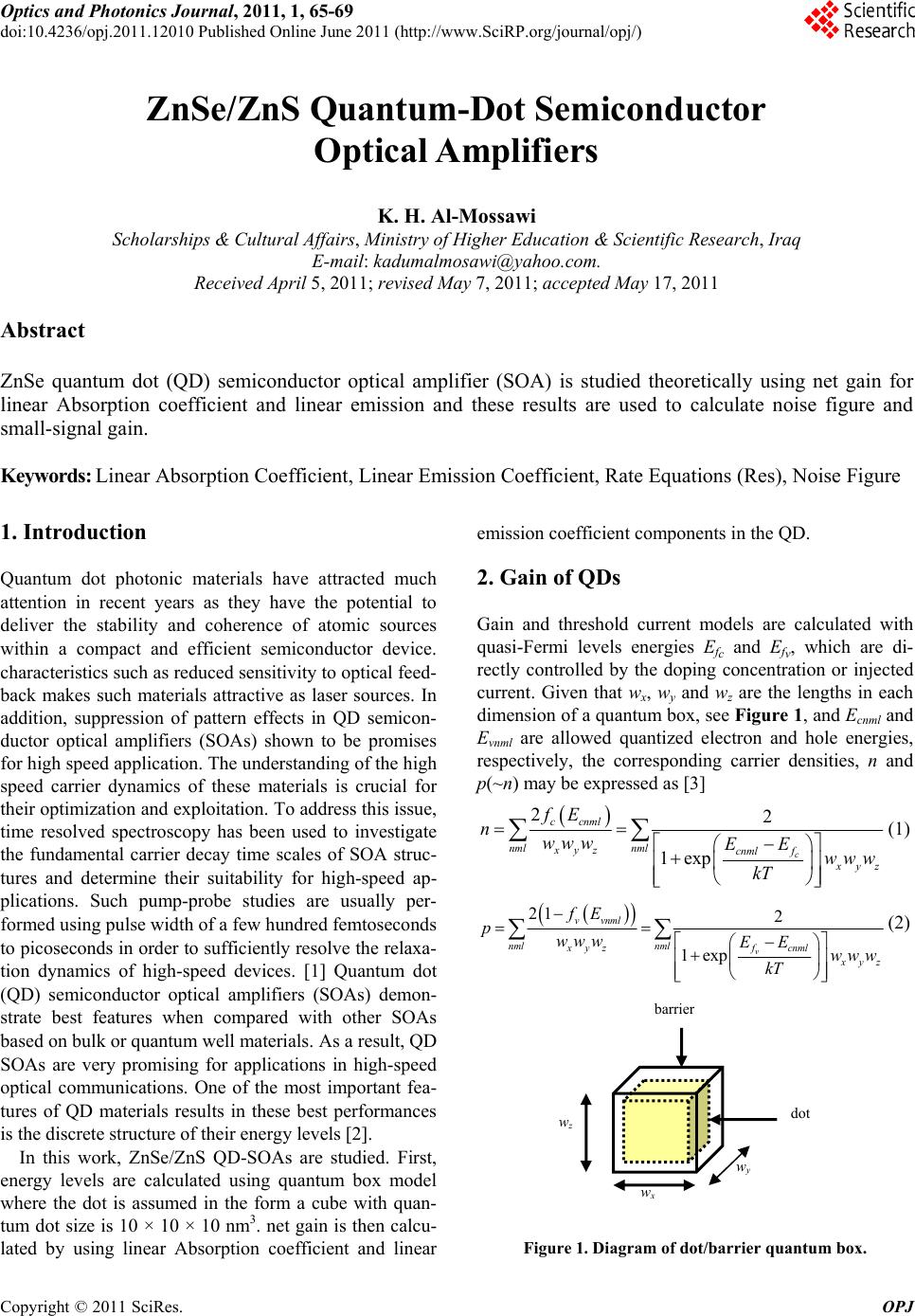 Optics and Photonics Journal, 2011, 1, 65-69 doi:10.4236/opj.2011.12010 Published Online June 2011 (http://www.SciRP.org/journal/opj/) Copyright © 2011 SciRes. OPJ ZnSe/ZnS Quantum-Dot Semiconductor Optical Amplifiers K. H. Al-Mossawi Scholarships & Cultural Affairs, Ministry of Higher Education & Scientific Research, Iraq E-mail: kadumalmosawi@yahoo.com. Received April 5, 2011; revised May 7, 2011; accepted May 17, 2011 Abstract ZnSe quantum dot (QD) semiconductor optical amplifier (SOA) is studied theoretically using net gain for linear Absorption coefficient and linear emission and these results are used to calculate noise figure and small-signal gain. Keywords: Linear Absorption Coefficient, Linear Emission Coefficient, Rate Equations (Res), Noise Figure 1. Introduction Quantum dot photonic materials have attracted much attention in recent years as they have the potential to deliver the stability and coherence of atomic sources within a compact and efficient semiconductor device. characteristics such as reduced sensitivity to optical feed- back makes such materials attractive as laser sources. In addition, suppression of pattern effects in QD semicon- ductor optical amplifiers (SOAs) shown to be promises for high speed application. The understanding of the high speed carrier dynamics of these materials is crucial for their optimization and exploitation. To address this issue, time resolved spectroscopy has been used to investigate the fundamental carrier decay time scales of SOA struc- tures and determine their suitability for high-speed ap- plications. Such pump-probe studies are usually per- formed using pulse width of a few hundred femtoseconds to picoseconds in order to sufficiently resolve the relaxa- tion dynamics of high-speed devices. [1] Quantum dot (QD) semiconductor optical amplifiers (SOAs) demon- strate best features when compared with other SOAs based on bulk or quantum well materials. As a result, QD SOAs are very promising for applications in high-speed optical communications. One of the most important fea- tures of QD materials results in these best performances is the discrete structure of their energy levels [2]. In this work, ZnSe/ZnS QD-SOAs are studied. First, energy levels are calculated using quantum box model where the dot is assumed in the form a cube with quan- tum dot size is 10 × 10 × 10 nm3. net gain is then calcu- lated by using linear Absorption coefficient and linear emission coefficient components in the QD. 2. Gain of QDs Gain and threshold current models are calculated with quasi-Fermi levels energies Efc and Efv, which are di- rectly controlled by the doping concentration or injected current. Given that wx, wy and wz are the lengths in each dimension of a quantum box, see Figure 1, and Ecnml and Evnml are allowed quantized electron and hole energies, respectively, the corresponding carrier densities, n and p(~n) may be expressed as [3] 22 1exp c c cnml nml nml xyz cnml f x yz fE nwww EE www kT (1) 21 2 1exp v vvnml nml nml xyz fcnml x yz fE pwww EE www kT (2) Figure 1. Diagram of dot/barrier quantum box. wx wy wz barrier dot 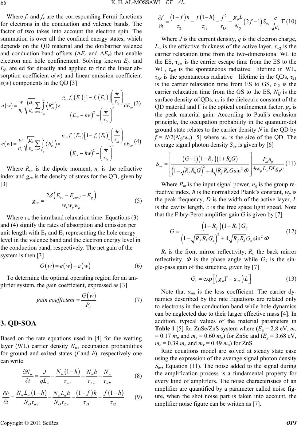 K. H. AL-MOSSAWI ET AL. Copyright © 2011 SciRes. OPJ 66 Where fc and fv are the corresponding Fermi functions for electrons in the conduction and valence bands. The factor of two takes into account the electron spin. The summation is over all the confined energy states, which depends on the QD material and the dot/barrier valence and conduction band offsets (ΔEc and ΔEv) that enable electron and hole confinement. Solving known Efc and Efv are ed for directly and applied to find the linear ab- sorption coefficient α(w) and linear emission coefficient e(w) components in the QD [3] 12 2 2 2 1 d g cv vc in o cv cv nml roE cv in h gf Ef E w aw RE nh Ehw (3) 21 2 2 2 1 d g cv cv in o cv cv nml roE cv in h gf Ef E w ew RE nh Ehw (4) Where Rcv is the dipole moment, nr is the refractive index and gcv is the density of states for the QD, given by [3] 2cv cnmlg cv xyz EE E gwww (5) Where τin the intraband relaxation time. Equations (3) and (4) signify the rates of absorption and emission per unit length with E1 and E2 representing the hole energy level in the valence band and the electron energy level in the conduction band, respectively. The net gain of the system is then [3] Gwew aw (6) To determine the optimal operating region for an am- plifier system, the gain coefficient, expressed as [3] in Gw gaincoefficientP (7) 3. QD-SOA Based on the rate equations used in [4] for the wetting layer (WL) carrier density Nw, occupation probabilities for ground and exited states (f and h), respectively one can write. 22 1 w www ww wwR Nh NNhN J tqL (8) 22 2112 111 ww ww QwQ w NLhf hfh NLh h tN N (9) 2 2112 1 11 21 p av RQ s gL fh fh ffc fS tN (10) Where J is the current density, q is the electron charge, Lw is the effective thickness of the active layer, τw2 is the carrier relaxation time from the two-dimensional WL to the ES, τ2w is the carrier escape time from the ES to the WL, τwR is the spontaneous radiative lifetime in WL, τ1R is the spontaneous radiative lifetime in the QDs, τ21 is the carrier relaxation time from ES to GS, τ12 is the carrier relaxation time from the GS to the ES, NQ is the surface density of QDs, εs is the dielectric constant of the QD material and Г is the optical confinement factor. gp is the peak material gain. According to Pauli's exclusion principle, the occupation probability in the quantum-dot ground state relates to the carrier density N in the QD by f = N/2(NQ/wx) [5] where wx is the size of the QD. The average signal photon density Sav is given by [6] 22 11 1 14sin fb in g av p wp fb fb GRRG Pn Shw L DLgc RRG RRG (11) Where Pin is the input signal power, ng is the group re- fractive index, ћ is the normalized Plank’s constant, wp is the peak frequency, D is the width of the active layer, L is the cavity length, c is the free space light speed. Note that the Fibry-Perot amplifier gain G is given by [7] 22 11 14sin fbS fbs fbs RRG G RRG RRG (12) Rf is the front mirror reflectivity, Rb the back mirror reflectivity. Φ is the phase angle while GS is the sin- gle-pass gain of the structure, given by [7] int exp sp GgaL (13) Note that αint is the loss coefficient. The carrier dy- namics described by the rate Equations are related only to electrons in the conduction band while hole dynamics can be neglected due to their larger effective mass [4]. In addition, typical values of the material parameters in Table 1 [5] for ZnSe/ZnS system where (Eg = 2.8 eV, me = 0.17 mo and mv = 0.60 mo) for ZnSe and (Eg = 3.68 eV, me = 0.39 mo and mv = 0.49 mo) for ZnS. Rate equations model are solved at steady state case using the expression of the average signal photon density Sav, Equation (11). The noise added to the signal during the amplification process is a fundamental property for every kind of amplifiers. The noise characteristics of an amplifier are quantified by a parameter called noise fig- ure, when the shot noise part is taken into account, the amplifier noise figure can be written as [7]. 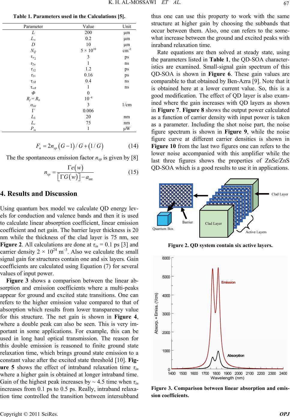 K. H. AL-MOSSAWI ET AL. Copyright © 2011 SciRes. OPJ 67 Table 1. Parameters used in the Calculations [5]. Parameter Value Unit L 200 μm Lw 0.2 μm D 10 μm NQ 5 × 1010 cm-2 τw2 3 ps τ2w 1 ns τ12 1.2 ps τ21 0.16 ps τ1R 0.4 ns τwR 1 ns Φ 0 Rf = Rb 10–4 αint 3 1/cm Γ 0.006 Lb 20 nm Lc 75 nm Pin 1 μW 21/1/ nsp F nG G G (14) The the spontaneous emission factor nsp is given by [8] int sp ew nGw a (15) 4. Results and Discussion Using quantum box model we calculate QD energy lev- els for conduction and valence bands and then it is used to calculate linear absorption coefficient, linear emission coefficient and net gain. The barrier layer thickness is 20 nm while the thickness of the clad layer is 75 nm, see Figure 2. All calculations are done at τin = 0.1 ps [3] and carrier density 2 × 1024 m–3. Also we calculate the small signal gain for structures contain one and six layers. Gain coefficients are calculated using Equation (7) for several values of input power. Figure 3 shows a comparison between the linear ab- sorption and emission coefficients where a multi-peaks appear for ground and excited state transitions. One can refers to the higher emission value compared to that of absorption which results from lower transparency value for this structure. The net gain is shown in Figure 4, where a double peak can also be seen. This is very im- portant in some applications. For example, this can be used in long haul optical transmission. The reason for this double emission is reasoned to finite ground state relaxation time, which brings ground state emission to a constant value after the excited state threshold [10]. Fig- ure 5 shows the effect of intraband relaxation time τin where a higher gain is obtained at longer intraband time. Gain of the highest peak increases by ~ 4.5 time when τin increases from 0.1 ps to 0.5 ps. Really, intraband relaxa- tion time controlled the transition between intersubband thus one can use this property to work with the same structure at higher gain by choosing the subbands that occur between them. Also, one can refers to the some- what increase between the ground and excited peaks with inraband relaxation time. Rate equations are then solved at steady state, using the parameters listed in Table 1, the QD-SOA character- istics are examined. Small-signal gain spectrum of this QD-SOA is shown in Figure 6. These gain values are comparable to that obtained by Ben-Azra [9]. Note that it is obtained here at a lower current value. So, this is a good modification. The effect of QD layer is also exam- ined where the gain increases with QD layers as shown in Figure 7. Figure 8 shows the output power calculated as a function of carrier density with input power is taken as a parameter. Including the shot noise part, the noise figure spectrum is shown in Figure 9, while the noise figure curve at different carrier densities is shown in Figure 10 from the last two figures one can refers to the lower noise accompanied with this amplifier while the last three figures shows the properties of ZnSe/ZnS QD-SOA which is a good results to use it in applications. Figure 2. QD system contain six active layers. Figure 3. Comparison between linear absorption and emis- sion coefficients. 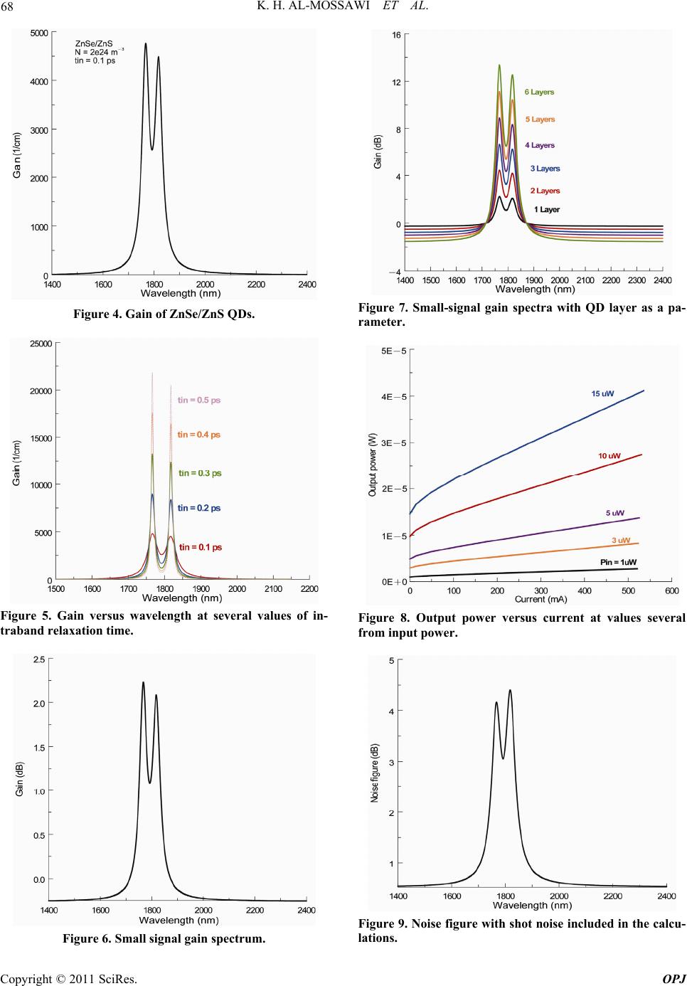 K. H. AL-MOSSAWI ET AL. Copyright © 2011 SciRes. OPJ 68 Figure 4. Gain of ZnSe/ZnS QDs. Figure 5. Gain versus wavelength at several values of in- traband relaxation time. Figure 6. Small signal gain spectrum. Figure 7. Small-signal gain spectra with QD layer as a pa- rameter. Figure 8. Output power versus current at values several from input power. Figure 9. Noise figure with shot noise included in the calcu- lations. 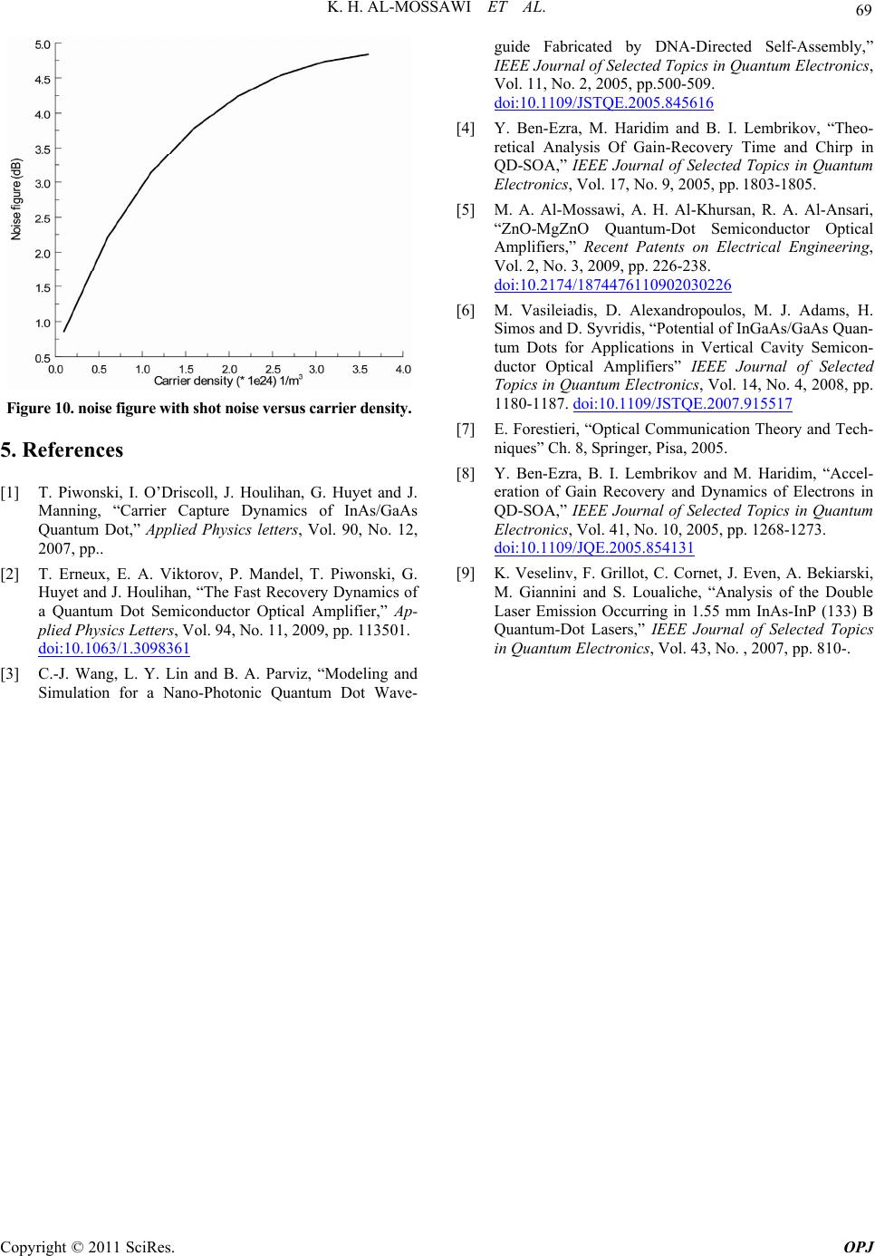 K. H. AL-MOSSAWI ET AL. Copyright © 2011 SciRes. OPJ 69 Figure 10. noise figure with shot noise versus carrier density. 5. References [1] T. Piwonski, I. O’Driscoll, J. Houlihan, G. Huyet and J. Manning, “Carrier Capture Dynamics of InAs/GaAs Quantum Dot,” Applied Physics letters, Vol. 90, No. 12, 2007, pp.. [2] T. Erneux, E. A. Viktorov, P. Mandel, T. Piwonski, G. Huyet and J. Houlihan, “The Fast Recovery Dynamics of a Quantum Dot Semiconductor Optical Amplifier,” Ap- plied Physics Letters, Vol. 94, No. 11, 2009, pp. 113501. doi:10.1063/1.3098361 [3] C.-J. Wang, L. Y. Lin and B. A. Parviz, “Modeling and Simulation for a Nano-Photonic Quantum Dot Wave- guide Fabricated by DNA-Directed Self-Assembly,” IEEE Journal of Selected Topics in Quantum Electronics, Vol. 11, No. 2, 2005, pp.500-509. doi:10.1109/JSTQE.2005.845616 [4] Y. Ben-Ezra, M. Haridim and B. I. Lembrikov, “Theo- retical Analysis Of Gain-Recovery Time and Chirp in QD-SOA,” IEEE Journal of Selected Topics in Quantum Electronics, Vol. 17, No. 9, 2005, pp. 1803-1805. [5] M. A. Al-Mossawi, A. H. Al-Khursan, R. A. Al-Ansari, “ZnO-MgZnO Quantum-Dot Semiconductor Optical Amplifiers,” Recent Patents on Electrical Engineering, Vol. 2, No. 3, 2009, pp. 226-238. doi:10.2174/1874476110902030226 [6] M. Vasileiadis, D. Alexandropoulos, M. J. Adams, H. Simos and D. Syvridis, “Potential of InGaAs/GaAs Quan- tum Dots for Applications in Vertical Cavity Semicon- ductor Optical Amplifiers” IEEE Journal of Selected Topics in Quantum Electronics, Vol. 14, No. 4, 2008, pp. 1180-1187. doi:10.1109/JSTQE.2007.915517 [7] E. Forestieri, “Optical Communication Theory and Tech- niques” Ch. 8, Springer, Pisa, 2005. [8] Y. Ben-Ezra, B. I. Lembrikov and M. Haridim, “Accel- eration of Gain Recovery and Dynamics of Electrons in QD-SOA,” IEEE Journal of Selected Topics in Quantum Electronics, Vol. 41, No. 10, 2005, pp. 1268-1273. doi:10.1109/JQE.2005.854131 [9] K. Veselinv, F. Grillot, C. Cornet, J. Even, A. Bekiarski, M. Giannini and S. Loualiche, “Analysis of the Double Laser Emission Occurring in 1.55 mm InAs-InP (133) B Quantum-Dot Lasers,” IEEE Journal of Selected Topics in Quantum Electronics, Vol. 43, No. , 2007, pp. 810-. |