Journal of Computer and Communications, 2015, 3, 49-55
Published Online March 2015 in SciRes. http://www.scirp.org/journal/jcc
http://dx.doi.org/10.4236/jcc.2015.33009
How to cite this paper: Rushingabigwi, G. and Sun, L.G. (2015) Design of an 868 MHz Printed S-Shape Monopole Antenna.
Journal of Computer and Communications, 3, 49-55. http://dx.doi.org/10.4236/jcc.2015.33009
Design of an 868 MHz Printed S-Shape
Monopole Antenna
Gerard Rushingabigwi, Liguo Sun
Depart ment of Electron ic Engineerin g and Information Science, Univ ersity of Scienc e and Technology of China
(USTC), H efei, China
Email: gerard @mail.u stc.edu. cn, liguos@ust c.edu.cn
Received January 2015
Copyright © 2015 by authors and Scientific Resear ch Publishing Inc.
This work is lic ens ed under the Creati ve Commons Attribution International License (CC BY).
http://creativ ecommon s.org/l icenses/by/4. 0/
Abstract
The purpose of this w ork is to des ign an d an al yz e an s-sh aped p rin te d ci rcuit bo ar d (PC B) m ono-
pole antenna. The antenna was analyz ed to op er at e at a resonance frequenc y band of 868 MHz ;
accep t abl e in 915 MHz as well. The s-shap e is selected due to the need of redu c ing the ove r all size
of the norm al mon opol e anten na. The printe d an tenna was desig ned with an approximate overall
size of 39 × 56 mm2 of whic h th e antenn a’s upper side is 26 × 39 mm2 wh il e i ts refe rence grou nd
board was sized at 39 × 30 mm2. The antenna is fed by a str ip line of 3 × 1.5 mm2, in series with a
4.4 pF cap aci t anc e and sh unt with an 8.7 nH ind uctance for purpose of antenna’s imped ance
matching with the input. A couple of existing publ ications showed tha t PCB antenna is not a ne w
technology; howev er not an old tec hnol og y for telecommu nicati on industr y. The raised probl em
by this work w as duly solved with HFSS as a tool; excellent results ar e present ed. After duly
matching the antenn a’s imped ance with 50 Ω micr os trip feed-l ine, solutions for overall perfo r-
mance were analyz ed and demonstr ated optimal: ra di ati on p at te rns we re pro ven omnidirec tional,
antenna gain optimized. The present a ntenn a pr ototyp e ’s ove ral l dim ensi ons ca n be readjusted
according to a ny indust rial and m anuf acturing requ ests.
Keywords
S-Shape, Printed Antenn a, HFSS, Impedanc e Ma tch in g
1. Introduction
Most monopole antennas commonly refer to quarter wavelengths (λ/4); der ivatives of dipoles where one element
is folded into the gro und (GND) and serves as the second rad iato r [1] [2]. The first deriv atives of the monopole
are the inverted-L and inverted-F ant ennas [3]-[6]. The ante nna length is an important parameter and it is influ-
enced by the dielectric cons tant of the material in the reactive near field. According to [2], calculation of the ef-
G. Rushingabigwi, L. G. Sun
50
fective dielectric co nstant
( )
eff
ε
for both the half-wave dipole and the quarter-wave monopole is approximated
in (1).
2
rr
eff
ε1ε11W
ε0.04 1
22 2
12 h
1W


+− 

=+×+ ×−

× 

+


(1)
where h is the thickness of substrate or PCB material; W is the trace width of the dipole arms, decided to 2 mm
in this case [7]-[11]. The working or effective wavelengt h
( )
eff
λ
for most ant ennas is then giv en by the formu-
la in (2),
eff
eff
λ
λ
ε
=
(2); knowing the free space wavelengt h,
0
c
λf
=
(3); whereby
is the
speed of light and f is the working frequency in Hertz (Hz).
2. The Proposed s-Shape Monopole Antenna Stru cture
As per Equations (1)-(3), normal monopole antennas to work with industrial, scientific and medical (ISM) band
of 868 MHz and 915 MHz would be presenting the length sizes according to Table 1.
None theless, irresp ective of the calculated lengths in Table 1, t he proposed s-shape antenna will utilize al-
most half of the overall length. It is to note that s-shape, snakelike shape as well as Meander shape are inter-
changeable names [2] [7]. The proposed s-shaped monopole antenna’s design model is illustrated in Fig ur e 1.
3. The Antenna Desig n, A nal ysis a nd Discussions
The software tool that was utilized for the design tasks is Ansoft HF SS [2]. According to the necessary problem
solving step s, the solution type for the present model is set to driven terminal. It normally calculates the termin-
al-based s-parameters of multi-conduc tor trans missio n line ports. The s-shaped monopole antenna element to-
gether with the feed-line as well as the ground boards (top and bottom) are all assigned with finite conduc tiv ity
boundary. It is one of the adv anced boundary conditions. The rectangular port designed at 0.8 × 1.5 mm2 is as-
signe d the lumped port excitation.
Table 1. Theoretical monopole lengths.
2.9931=
eff
ε
on a 0.8 mm thick FR-4 PCB,
4.4=
r
ε
Frequency (MHz)
0
λ
(mm)
eff
λ
(mm)
eff
λ
4
(mm)
eff
λ
2
(mm)
868
345.6
199.7
50
100
915
327.8
189.5
47.4
94.8
Figure 1. The proposed antenna structure.
G. Rushingabigwi, L. G. Sun
51
3.1. Design Results
3.1.1. The A ntenna ’s Retur n Los s (RL)
As a meas ure of the reflected energy from a transmitted signal, Figure 2 illus tra tes the maximum RL of 7.76
dB at 868 MHz.
It is practically known tha t the bigger the value of RL, the much less energy reflected back; the main reason
of this kind of loss is due to mismatch conditio ns of the antenna with the input impedance. For that reaso n, the
impedance matching will be applied which will reach to optimization results.
3.1.2. The Ante nna’s Impedance
The impedance analysis by Smith Chart in Figure 3 results in mismatch where t he point m1 is ver y far from the
matching point.
Figure 2. The return lo ss (RL) before impedan ce matchi ng, resonance at 868 MHZ.
Figure 3. Smith chart impedance analysis.
0.400.50 0.60 0.700.800.90 1.00 1.10 1.20
Freq [GHz]
-8.00
-7.00
-6.00
-5.00
-4.00
-3.00
-2.00
-1.00
0.00
dB(St(T1,T1))
HFSSDesign1
XY Plot 1
ANSOFT
m1
Curve Info
dB(St(T1,T1))
Setup1 : Sweep
Name X Y
m1 0.8680 -7.7588
G. Rushingabigwi, L. G. Sun
52
Reading the current Smith Chart in Figure 3, the actual antenna impedance is give n by the calculation of the
normalized input impedances,
in
Z
, such that
( )
in
Z0.47660.331 *5023.83j16.5+=+=
; which give us values
for the real and imaginary parts to be used during the Smith Chart impedance matching in Figure 4.
3.2. Impedance Matching
The Smith Chart impedance matching data points 1, 2 and 3 respectively, in Figure 4(a), were obtained by fix-
ing a central frequency of 868 MHz, thus generating point 1; then by drawing a series capacitance from point 1
to point 2 and finally drawing a shunt inductance from point 2 to point 3. This means the pullin g of antenna’s
impedance to the central matching point. Under such conditions, the Smith chart syste m c alculates the matching
series capacitance to 4.4 pF while the shunt inductance is 8.7 nH as shown in Figure 4(b). The value s are t hen
implemented into the 3D model of Figure 1 as R-L-C impedance matching circuit, R = 50 Ω be ing the strip
feed-line’s resistance.
3.3. Optimization Results
Afte r building the ma tching circuit as shown in Figure 1, the new simulation results were considered optimal as
presented in Figures 5-9. Those are Smith Char t impedance, radiation patterns, return loss and PCB fields over-
lay respectively. Regarding the capacitance and induct ance siz e s, the real implementatio n would adopt the stan-
dard manufacturing smaller sizes of such valued capacitance and i nductance.
3.4. Discussions
According to the standards [8]-[11], the impedance matching [12] [13] bri ngs a big improvement. For example,
due to that impedance matc hing in our model, the return loss shifts from 7.76 dB to 16.5 dB. Another proof is
the measurement by Smith Chart in Figure 5 which show the very big difference between unmatched conditions
illustrated in Figure 3. Observing the return loss beha vior in Fig ur e 8, the 6.15 dB bandwidth is estimated to
(0.915 - 0.826) MHz = 0.089 MHz; while for the 16.5 dB bandwidth is estimated to 0 MHz.
4. Conclusion
The PCB monopole s-shaped antenna design and si mulat ion have been so s uccessful that the obtained resul ts are
excellent, notably the omonidirectional radiation patterns shown in Figures 7-9. Due to the folding of the normally
(a) (b)
Fig ure 4. (a) Smith chart impedance matching; (b) Smith chart impedan ce matching sch emati c
diagr a m.
G. Rushingabigwi, L. G. Sun
53
Figure 5. Impedance measuring by smith chart.
Figure 6. EH plane radiation pattern.
G. Rushingabigwi, L. G. Sun
54
Figure 7. 3D radiation pattern.
Figure 8. Return loss.
Antenna
20
40(mm)
50(mm)
25
0
Antenna
Figure 9. Th e PCB fields overlaying in two different view positions.
G. Rushingabigwi, L. G. Sun
55
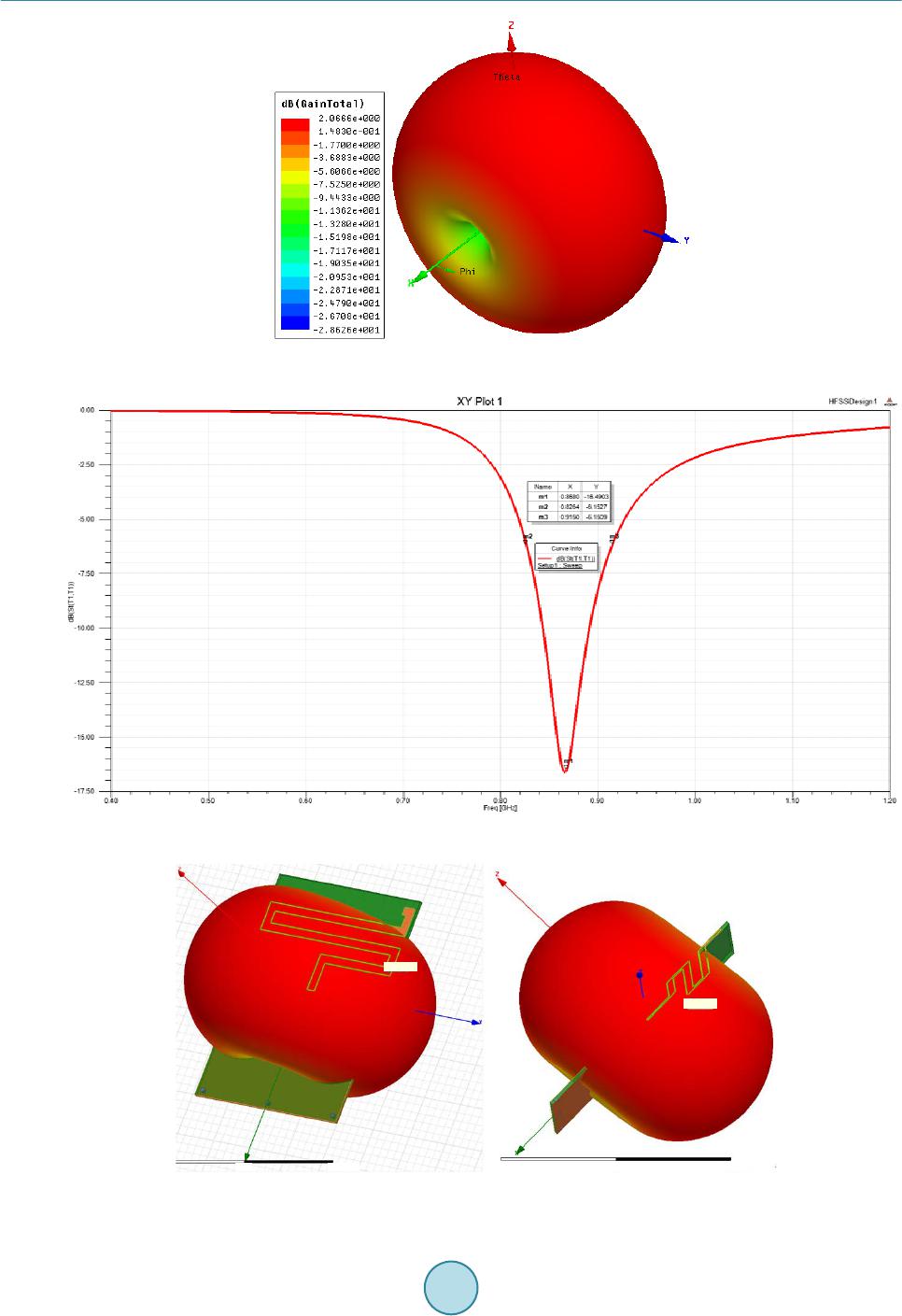
known monopole antenna into a snakelike shape, the antenna has reached to a r educed size that can be easily
implemented in all miniaturized transceivers and receivers operating in ISM 868MHz as well as in ISM 915
MHz with less return loss.
Acknowledgements
A lo t of gratitude is addressed to the Go vernment of People’s Republic of China to have supported and streng-
thened engineering researc h ac tivitie s in the University of Science and Technology of China.
References
[1] Q i wu, T. and Erricolo, D. (2007) Comparison between Printed Folded Monopole and Inverted F Antennas for Wireless
Portable Devices. Antennas and Propagation Society International Symposium, 4701-4704 .
http://dx.doi.org/10.1109/APS.2007.4396593
[2] Mi n gyang, L. and Liu , M. (2014) Monopole Antenna and Dipole Antenna Design in HFSS Antenna Design. Chapter 3,
2nd Edition, Publishing House of Electronics Industry, Beijing, 22-43.
[3] Mat thew, L. an d Ib ou n, S. (20 05) ISM-Ban d and S hor t Ran ge Device Antennas. Texas InstrumentsApplication Re-
port Swra046a, 1-37. http://wenku.baidu.com/view/71b8d0126edb6f1aff001f8f.html
[4] Ni, W. and Nakaji ma, N. (2010) Smal l P rin t e d Invert ed-L Mon opo le Antenna for Worldwide Interoperability for Mi-
crowa v e Access Wideband Operation. IET Microwaves, Antennas & Propagation, 4, 1714-1719.
http://dx.doi.org/10.1049/iet-map.2009.0469
[5] Chen , H.-D., Chen, J.-S. and Cheng, Y.-T. (2003) Modified In verted-L Monopole Antenna for 2.4 /5 GH z Du al-Band
Operations. IEEE Electron ics Letters, 39, 1567-1568. http://dx.doi.org/10.1049/el:20031037
[6] So ras, C., et al. ( 2002 ) Analysis and Design of an Inverted-F Antenna Printed on a PCMCIA Card for the 2.4 GHz ISM
Band. I EE E Antennas Propagat Mag., 44, 37-44. http://dx.doi.org/10.1109/74.997891
[7] Riad , K. (2014) Compact Double Meandered Li n e In verted-F Antenna for Outdo o r P arki ng Wireless Car Dete cto r.
IEEE Asia Pacific Conference on Wireless and Mobile, 30-35. http://dx.doi.org/10.1109/APWiMob.2014.6920279
[8] Fredrik, K. (2009 ) 868 MHz, 915 MHz, and 955 MHz Monopo le PCB Antenna. Texas Instruments Design Note
DN024 Swra227d, 1-15. http://wenku.baidu.com/view/a17c353231126edb6f1a1071.html
[9] Audun, A. (2009) 868 MHz, 915 MHz and 955 MHz Monopole PCB Antenna. Texas Inst rumentsDesign Note DN00 8,
1-16. http://www.docin.com/p-672547 83 5.h tml
[10] Rich ard, W. (2013) Monopole PCB Antenna with Single or Dual Band Option. Texas Inst ruments De s i gn No te DN024,
1-16. http://www.ti.com/lit/an/swra227e/swra227e.pdf
[11] Rich ard, W. (20 10 ) Antenna Selection Guide. Texas InstrumentsApplication Note A N0 5 8, 1-44.
http://www.ti.com.cn/cn/lit/an/swra161b/swra161b.pdf
[12] Marro cco, G. (2008) The Art Of UHF RFID Antenna Design: I mped ance Mat chin g and Si ze Reduc ti on Techniques.
IEEE Antennas and Propagation Magazine, 50, 66-79. http: //d x.doi .o rg/ 10. 11 09/ MAP. 20 08. 4494 504
[13] Zuffanelli, S., et al. (2014) An Impedan ce Matchi ng Method for Opt ical Disc-Based UHF-RFID Ta gs . IEEE Intern a-
tional Conferen ce on RFID, 15-22 . http://dx.doi.org/10.1109/RFID.2014.681070