Paper Menu >>
Journal Menu >>
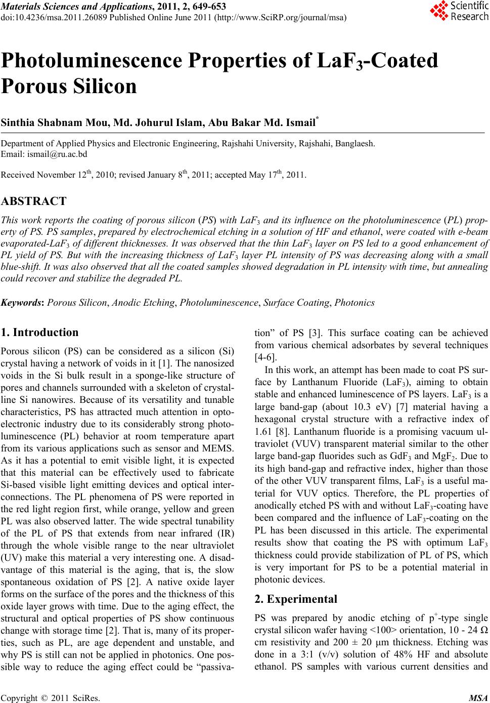 Materials Sciences and Applicatio ns, 2011, 2, 649-653 doi:10.4236/msa.2011.26089 Published Online June 2011 (http://www.SciRP.org/journal/msa) Copyright © 2011 SciRes. MSA 649 Photoluminescence Properties of LaF3-Coated Porous Silicon Sinthia Shabnam Mou, Md. Johurul Islam, Abu Bakar Md. Ismail* Department of Applied Physics and Electronic Engineering, Rajshahi University, Rajshahi, Banglaesh. Email: ismail@ru.ac.bd Received November 12th, 2010; revised January 8th, 2011; accepted May 17th, 2011. ABSTRACT This work reports the coating of porous silicon (PS) with LaF3 and its influence on the photoluminescence (PL) prop- erty of PS. PS samples, prepared by electrochemical etching in a solution of HF and ethanol, were coated with e-beam evaporated-LaF3 of different thicknesses. It was observed that the thin LaF3 la yer on PS led to a good enhancement of PL yield of PS. But with the increasing thickness of LaF3 layer PL intensity of PS was decreasing along with a small blue-shift. It was also observed that all the coa ted samples showed degradation in PL intens ity with time, but annealing could recover and stabilize the d egra ded PL. Keywords: Porous Silicon, Anodic Etching, Photoluminescence , S urf ace C oat i n g, Photonics 1. Introduction Porous silicon (PS) can be considered as a silicon (Si) crystal having a network of voids in it [1]. The nanosized voids in the Si bulk result in a sponge-like structure of pores and channels surrounded with a skeleton of crystal- line Si nanowires. Because of its versatility and tunable characteristics, PS has attracted much attention in opto- electronic industry due to its considerably strong photo- luminescence (PL) behavior at room temperature apart from its various applications such as sensor and MEMS. As it has a potential to emit visible light, it is expected that this material can be effectively used to fabricate Si-based visible light emitting devices and optical inter- connections. The PL phenomena of PS were reported in the red light region first, while orange, yellow and green PL was also observed latter. The wide spectral tunability of the PL of PS that extends from near infrared (IR) through the whole visible range to the near ultraviolet (UV) make this material a very interesting one. A disad- vantage of this material is the aging, that is, the slow spontaneous oxidation of PS [2]. A native oxide layer forms on the surface of the pores and the thickness of this oxide layer grows with time. Due to the aging effect, the structural and optical properties of PS show continuous change with storage time [2]. That is, many of its proper- ties, such as PL, are age dependent and unstable, and why PS is still can not be applied in photonics. One pos- sible way to reduce the aging effect could be “passiva- tion” of PS [3]. This surface coating can be achieved from various chemical adsorbates by several techniques [4-6]. In this work, an attempt has been made to coat PS sur- face by Lanthanum Fluoride (LaF3), aiming to obtain stable and enhanced luminescence of PS layers. LaF3 is a large band-gap (about 10.3 eV) [7] material having a hexagonal crystal structure with a refractive index of 1.61 [8]. Lanthanum fluoride is a promising vacuum ul- traviolet (VUV) transparent material similar to the other large band-gap fluorides such as GdF3 and MgF2. Due to its high band-gap and refractive index, higher than those of the other VUV transparent films, LaF3 is a useful ma- terial for VUV optics. Therefore, the PL properties of anodically etched PS with and without LaF3-coating have been compared and the influence of LaF3-coating on the PL has been discussed in this article. The experimental results show that coating the PS with optimum LaF3 thickness could provide stabilization of PL of PS, which is very important for PS to be a potential material in photonic devices. 2. Experimental PS was prepared by anodic etching of p+-type single crystal silicon wafer having <100> orientation, 10 - 24 Ω cm resistivity and 200 ± 20 μm thickness. Etching was done in a 3:1 (v/v) solution of 48% HF and absolute ethanol. PS samples with various current densities and 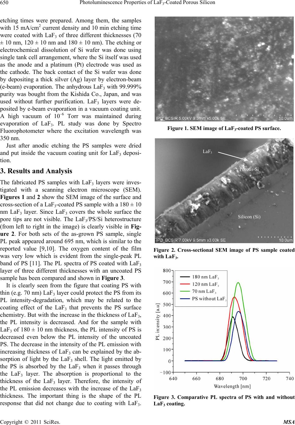 Photoluminescence Properties of LaF-Coated Porous Silicon 650 3 etching times were prepared. Among them, the samples with 15 mA/cm2 current density and 10 min etching time were coated with LaF3 of three different thicknesses (70 ± 10 nm, 120 ± 10 nm and 180 ± 10 nm). The etching or electrochemical dissolution of Si wafer was done using single tank cell arrangement, where the Si itself was used as the anode and a platinum (Pt) electrode was used as the cathode. The back contact of the Si wafer was done by depositing a thick silver (Ag) layer by electron-beam (e-beam) evaporation. The anhydrous LaF3 with 99.999% purity was bought from the Kishida Co., Japan, and was used without further purification. LaF3 layers were de- posited by e-beam evaporation in a vacuum coating unit. A high vacuum of 10–6 Torr was maintained during evaporation of LaF3. PL study was done by Spectro Fluorophotometer where the excitation wavelength was 350 nm. Just after anodic etching the PS samples were dried and put inside the vacuum coating unit for LaF3 deposi- tion. 3. Results and Analysis The fabricated PS samples with LaF3 layers were inves- tigated with a scanning electron microscope (SEM). Figures 1 and 2 show the SEM image of the surface and cross-section of a LaF3-coated PS sample with a 180 ± 10 nm LaF3 layer. Since LaF3 covers the whole surface the pore tips are not visible. The LaF3/PS/Si heterostructure (from left to right in the image) is clearly visible in Fig- ure 2. For both sets of the as-grown PS sample, single PL peak appeared around 695 nm, which is similar to the reported value [9,10]. The oxygen content of the film was very low which is evident from the single-peak PL band of PS [11]. The PL spectra of PS coated with LaF3 layer of three different thicknesses with an uncoated PS sample has been compared and shown in Figure 3. It is clearly seen from the figure that coating PS with thin (e.g. 70 nm) LaF3 layer could protect the PS from its PL intensity-degradation, which may be related to the coating effect of the LaF3 that prevents the PS surface chemistry. But with the increase in the thickness of LaF3, the PL intensity is decreased. And for the sample with LaF3 of 180 ± 10 nm thickness, the PL intensity of PS is decreased even below the PL intensity of the uncoated PS. The decrease in the intensity of the PL emission with increasing thickness of LaF3 can be explained by the ab- sorption of light by the LaF3 shell. The light emitted by the PS is absorbed by the LaF3 when it passes through the LaF3 layer. The absorption is proportional to the thickness of the LaF3 layer. Therefore, the intensity of the PL emission decreases with the increase of the LaF3 thickness. The important thing is the shape of the PL response that did not change due to coating with LaF3. Figure 1. SEM image of LaF3-coated PS surface. Silicon (Si) Porous-Si LaF 3 Figure 2. Cross-sectional SEM image of PS sample coated with LaF3. Figure 3. Comparative PL spectra of PS with and without LaF3 coating. Copyright © 2011 SciRes. MSA 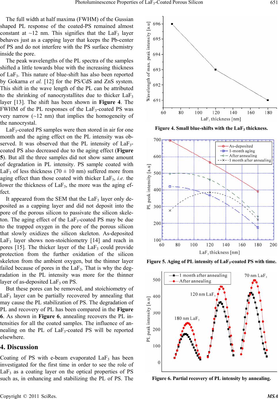 Photoluminescence Properties of LaF-Coated Porous Silicon651 3 The full width at half maxima (FWHM) of the Gussian shaped PL response of the coated-PS remained almost constant at ~12 nm. This signifies that the LaF3 layer behaves just as a capping layer that keeps the Pb-center of PS and do not interfere with the PS surface chemistry inside the pore. The peak wavelengths of the PL spectra of the samples shifted a little towards blue with the increasing thickness of LaF3. This nature of blue-shift has also been reported by Gokarna et al. [12] for the PS/CdS and ZnS system. This shift in the wave length of the PL can be attributed to the shrinking of nanocrystallites due to thicker LaF3 layer [13]. The shift has been shown in Figure 4. The FWHM of the PL responses of the LaF3-coated PS was very narrow (~12 nm) that implies the homogeneity of the nanocrystal. LaF3-coated PS samples were then stored in air for one month and the aging effect on the PL intensity was ob- served. It was observed that the PL intensity of LaF3- coated PS also decreased due to the aging effect (Figure 5). But all the three samples did not show same amount of degradation in PL intensity. PS sample coated with LaF3 of less thickness (70 ± 10 nm) suffered more from aging effect than those coated with thicker LaF3, i.e. the lower the thickness of LaF3, the more was the aging ef- fect. It appeared from the SEM that the LaF3 layer only de- posited as a capping layer and did not deposit into the pore of the porous silicon to passivate the silicon skele- ton. The aging effect of the LaF3-coated PS may be due to the trapped oxygen in the pore of the porous silicon that slowly oxidizes the silicon skeleton. As-deposited LaF3 layer shows non-stoichiometry [14] and reach in pores [15]. The thicker layer of the LaF3 could provide protection from the further oxidation of the silicon skeleton from the ambient oxygen, but the thinner layer failed because of pores in the LaF3. That is why the deg- radation in the PL intensity was more for the thinner layer of as-deposited LaF3 on PS. But these pores can be removed, and stoichiometry of LaF3 layer can be partially recovered by annealing that may cause the PL stabilization of PS. The degradation of PL and recovery of PL has been compared in the Figure 6. As shown in Figure 6, annealing recovers the PL in- tensities for all the coated samples. The influence of an- nealing on the PL of LaF3-coated PS will be reported elsewhere. 4. Discussion Coating of PS with e-beam evaporated LaF3 has been investigated for the first time in order to see the role of LaF3 as a coating layer on the optical properties of PS such as, in enhancing and stabilizing the PL of PS. The Figure 4. Small blue-shifts with the LaF3 thickness. Figure 5. Aging of PL intensity of LaF3-coated PS with time. Figure 6. Partial recovery of PL intensity by annealing. Copyright © 2011 SciRes. MSA  Photoluminescence Properties of LaF-Coated Porous Silicon 652 3 thickness of the LaF3 appeared to have an important in- fluence on the PL characteristics of PS. Thinner layer of LaF3 could enhance the PL intensity without destroying the Gaussian shape of the PL response. This enhance- ment of PL is believed to be due to the coating effect of LaF3 that prevented oxidation of PS. But thicker layer of LaF3 lowered the PL intensity that may be due to the degradation of refractive index of the LaF3 layer induced by the mechanical stress which depends on the film thickness. The LaF3-coated un-annealed samples showed aging on the PL intensity. Generally the as-deposited evaporated LaF3 layer contains pores which when ex- posed to the air water vapor enters into the pore due to capillarity. This water vapor replaces the Si-H bonds with Si-O bond which seems responsible for the degrada- tion of the PL intensity. As the thicker layer of as-deposited LaF3 contains more water vapor the degra- dation of PL intensity was more. When the coated sam- ples were annealed at 400˚C for 10 minutes the PL inten- sity was partially recovered and the degradation of the recovered PL intensity was minimum for PS cited with thicker LaF3 layer. Experimental results suggest that coating PS with e-beam evaporated LaF3 and subsequent annealing could enable the PS to have an enhanced and stable PL. 5. Conclusions All the studies done in this work can be summarized as; coating PS with LaF3 of optimum thickness followed by annealing could lead to better luminous stability of PS. From these experimental results it can be concluded that coating with LaF3 of optimum thickness could provide the PS an enhanced and stable photoluminescence that will enable its use in the fabrication of optical devices, such as light-emitting diodes (LED), lasers and solar cells. 6. Acknowledgements The authors wish to thank the COMSTEC, TWAS, Tri- este, Italy, the Bangladesh University Grants Commis- sion, and the Faculty of Science of Rajshahi University for providing financial assistance. REFERENCES [1] A. G. Cullis, L. T. Canham and P. D. J. Calcott, “The Structural and Luminescence Properties of Porous Sili- con,” Journal of Applied Physics, Vol. 82, No. 3, 1997, pp. 909-965. doi:10.1063/1.366536 [2] R. Boukherroub, S. Morin, D. D. M. Wayner and D. J. Lockwood, “Thermal Route for Chemical Modification and Photoluminescence Stabilization of Porous Silicon,” Physical Status Solidi (A), Vol. 182, No. 1, 2000, pp 117- 121. doi:10.1002/1521-396X(200011)182:1<117::AID-PSSA1 17>3.0.CO;2-3 [3] B. Gelloz, H. Sano, R. Boukherroub, D. D. M. Wayner, D. J. Lockwood and N. Koshida, “Stabilization of Porous Silicon Electroluminescence by Surface Passivation with Controlled Covalent Bonds,” Applied Physics Letters, Vol. 83, No. 12, 2003, pp. 2342-2344. doi:10.1063/1.1613812 [4] R. Prabakaran, M. Peres, T. Monteiro, E. Fortunato, R. Martins and I. Ferreira, “The Effects of ZnO Coating on the Photoluminescence Properties of Porous Silicon for the Advanced Optoelectronic Devices,” Journal of Non-Crystalline Solids, Vol. 354, No. 19-25, 2008, pp. 2181-2185. [5] M. Rahmani, A. Moadhen, M.-A. Zaïbi, H. Elhouichet and M. Oueslati, “Photoluminescence Enhancement and Stabilisation of Porous Silicon Passivated by Iron,” Journal of Luminescence, Vol. 128, No. 11, 2008, pp. 1763-1766. doi:10.1016/j.jlumin.2008.04.003 [6] A. G. Macedo, E. A. De Vasconcelos, R. Valaski, F. Muchenski, E. F. Da Silva Jr., A. F. Da Silva and L. S. Roman, “Enhanced Lifetime in Porous Silicon Light- Emitting Diodes with Fluorine Doped Tin Oxide Elec- trodes,” Thin Solid Films, Vol. 517, No. 2, 2008, pp. 870- 873. doi:10.1016/j.tsf.2008.07.007 [7] E. D. Thoma, H. Shields, Y. Zhang, B. C. McCollum, R. T. Williams and J. Lumin, “EPR and Luminescence Studies of LaF3 and CeF3 under X-Ray and Laser Irradia- tion,” Journal of Luminescence, Vol. 71, No. 2, 1997, pp. 93-104. doi:10.1016/S0022-2313(97)81621-3 [8] D. R. Lide, “Physical Constants of Organic Compounds, in: CRC Handbook of Chemistry and Physics,” 87th Edi- tion, Taylor and Francis, Boca Raton, 2007. [9] H. J. Li, J. C. Peng, S. Qu, Y. H. Yan, X. M. Xu and C. J. Zhao, “Efficient Visible Porous Silicon Diodes Passivated by Carbon Films,” Chinese Physics Letters, Vol. 19, No. 7, 2002, pp. 1013-1015. doi:10.1088/0256-307X/19/7/341 [10] D. A. Kim, J.-H. Shim and N.-H. Cho, “PL and EL Fea- tures of P-Type Porous Silicon Prepared by Electro- chemical Anodic Etching,” Applied Surface Science, Vol. 234, No. 1-4, 2004, pp. 256-261. doi:10.1016/j.apsusc.2004.05.028 [11] M. Ohmukai, M. Taniguchi and Y. Tsutsumi, “Large current Density and Anodization Time Needed for Strong Photoluminescence in Porous Silicon,” Materials Science and Engineering B, Vol. 86, No. 1, 2001, pp. 26-29. doi:10.1016/S0921-5107(01)00635-3 [12] A. Gokarna, S. V. Bhoraskar, N. R. Pavaskar and S. D. Sathaye, “Optoelectronic Characterization of Porous Silicon/CdS and ZnS Systems,” Physica Status Solidi (A), Vol. 182, No. 1, 2000, pp. 175-179. doi:10.1002/1521-396X(200011)182:1<175::AID-PSSA1 75>3.0.CO;2-O [13] L. K. Pan, Y. K. Ee, C. Q. Sun, G. Q. Yu, Q. Y. Zhang and B. K. Tay, “Band-Gap Expansion, Core-Level Shift, and Dielectric Suppression of Porous Silicon Passivated by Plasma Fluorination,” Journal of Vacuum Science & Technology B, Vol. 22, No. 2, 2004, pp. 583-587. Copyright © 2011 SciRes. MSA  Photoluminescence Properties of LaF3-Coated Porous Silicon Copyright © 2011 SciRes. MSA 653 doi:10.1116/1.1651108 [14] T. Katsube, M. Hara and I. Serizawa, “MOS-Type Mi- cro-Oxygen Sensor Using LaF3 Workable at Room Tem- perature,” Japanese Journal of Applied Physics, Vol. 29, No. 8, 1990, pp. L1392-L395. [15] M. C. Liu, C. C. Lee, M. Kaneko, K. Nakahira and Y. Takano, “Microstructure Related Properties of Lantha- num Fluoride Films Deposited by Molybdenum Boat Evaporation at 193 nm,” Thin Solid Films, Vol. 492, No. 1-2, 2005, pp. 45-49. |