Paper Menu >>
Journal Menu >>
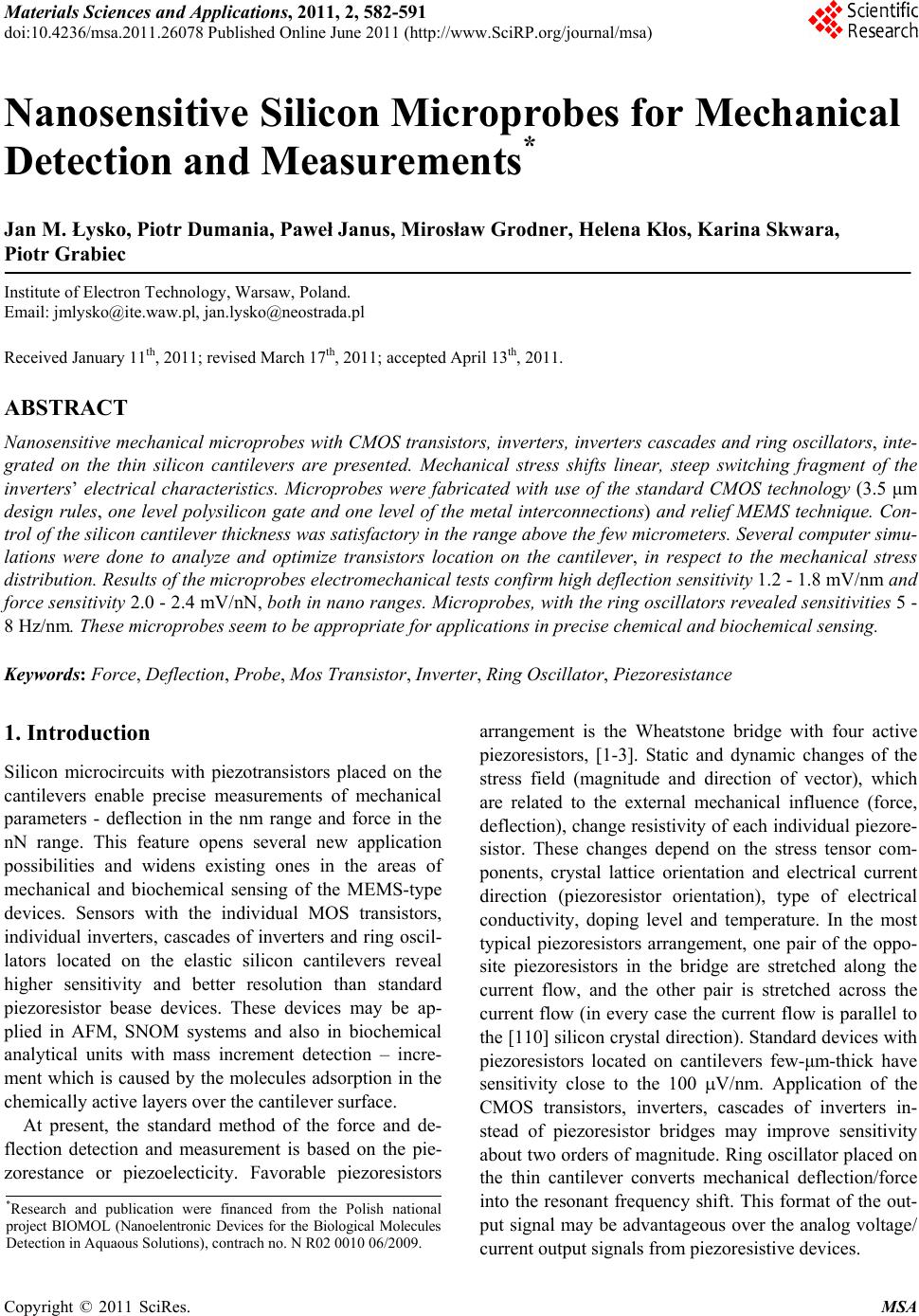 Materials Sciences and Applicatio ns, 2011, 2, 582-591 doi:10.4236/msa.2011.26078 Published Online June 2011 (http://www.SciRP.org/journal/msa) Copyright © 2011 SciRes. MSA Nanosensitive Silicon Microprobes for Mechanical Detection and Measurements* Jan M. Łysko, Piotr Dumania, Paweł Janus, Mirosław Grodner, Helena Kłos, Karina Skwara, Piotr Grabiec Institute of Electron Technology, Warsaw, Poland. Email: jmlysko@ite.waw.pl, jan.lysko@neostrada.pl Received January 11th, 2011; revised March 17th, 2011; accepted April 13th, 2011. ABSTRACT Nanosensitive mechanica l microprobes with CMOS transistors, inverters, inverters cascades and ring oscillato rs, inte- grated on the thin silicon cantilevers are presented. Mechanical stress shifts linear, steep switching fragment of the inverters’ electrical characteristics. Microprobes were fabricated with use of the standard CMOS technology (3.5 μm design rules, one level polysilicon gate and one level of the metal interconnections) and relief MEMS technique. Con- trol of the silicon cantilever thickness was satisfactory in the range above the few micrometers. Several computer simu- lations were done to analyze and optimize transistors location on the cantilever, in respect to the mechanical stress distribution. Results o f the microprobes electromecha nical tests co nfirm high deflectio n sen sitivity 1.2 - 1.8 mV/nm and force sensitivity 2.0 - 2.4 mV/nN, both in nano ranges. Microprobes, with the ring oscillato rs revealed sen sitivities 5 - 8 Hz/nm. These microprobes seem to be appropriate for applications in precise chemical and biochemical sensing. Keywords: Force, Deflection, Probe, Mos Transistor, Inverter, Ring Oscillator, Piezoresistance 1. Introduction Silicon microcircuits with piezotransistors placed on the cantilevers enable precise measurements of mechanical parameters - deflection in the nm range and force in the nN range. This feature opens several new application possibilities and widens existing ones in the areas of mechanical and biochemical sensing of the MEMS-type devices. Sensors with the individual MOS transistors, individual inverters, cascades of inverters and ring oscil- lators located on the elastic silicon cantilevers reveal higher sensitivity and better resolution than standard piezoresistor bease devices. These devices may be ap- plied in AFM, SNOM systems and also in biochemical analytical units with mass increment detection – incre- ment which is caused by the molecules adsorption in the chemically active layers over the cantilever surface. At present, the standard method of the force and de- flection detection and measurement is based on the pie- zorestance or piezoelecticity. Favorable piezoresistors arrangement is the Wheatstone bridge with four active piezoresistors, [1-3]. Static and dynamic changes of the stress field (magnitude and direction of vector), which are related to the external mechanical influence (force, deflection), change resistivity of each individual piezore- sistor. These changes depend on the stress tensor com- ponents, crystal lattice orientation and electrical current direction (piezoresistor orientation), type of electrical conductivity, doping level and temperature. In the most typical piezoresistors arrangement, one pair of the oppo- site piezoresistors in the bridge are stretched along the current flow, and the other pair is stretched across the current flow (in every case the current flow is parallel to the [110] silicon crystal direction). Standard devices with piezoresistors located on cantilevers few-μm-thick have sensitivity close to the 100 V/nm. Application of the CMOS transistors, inverters, cascades of inverters in- stead of piezoresistor bridges may improve sensitivity about two orders of magnitude. Ring oscillator placed on the thin cantilever converts mechanical deflection/force into the resonant frequency shift. This format of the out- put signal may be advantageous over the analog voltage/ current output signals from piezoresistive devices. *Research and publication were financed from the Polish national p roject BIOMOL (Nanoelentronic Devices for the Biological Molecules Detection in Aquaous Solutions), contrach no. N R02 0010 06/2009. 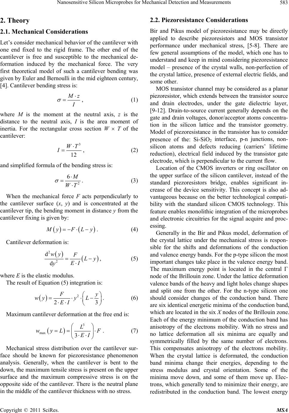 Nanosensitive Silicon Microprobes for Mechanical Detection and Measurements583 2. Theory 2.1. Mechanical Considerations Let’s consider mechanical behavior of the cantilever with one end fixed to the rigid frame. The other end of the cantilever is free and susceptible to the mechanical de- formation induced by the mechanical force. The very first theoretical model of such a cantilever bending was given by Euler and Bernoulli in the mid eighteen century, [4]. Cantilever bending stress is: M z I , (1) where M is the moment at the neutral axis, z is the distance to the neutral axis, I is the area moment of inertia. For the rectangular cross section W T of the cantilever: 3 12 WT I , (2) and simplified formula of the bending stress is: 2 6 M WT . (3) When the mechanical force F acts perpendicularly to the cantilever surface (x, y) and is concentrated at the cantilever tip, the bending moment in distance y from the cantilever fixing is given by: M yFLy . (4) Cantilever deformation is: 2 2 d d wy FLy EI y , (5) where E is the elastic modulus. The result of Equation (5) integration is: 2 23 F y wyy L EI . (6) Maximum cantilever deformation at the free end is: 3 max 3 L wyL F EI . (7) Mechanical stress distribution over the cantilever sur- face should be known for piezoresistance phenomenon analysis. Generally, when the cantilever is bent to the down, the maximum tensile stress is present on the upper surface and the maximum compressive stress is on the opposite side of the cantilever. There is the neutral plane in the middle of the cantilever thickness with no stress. 2.2. Piezoresistance Considerations Bir and Pikus model of piezoresistance may be directly applied to describe piezoresistors and MOS transistor performance under mechanical stress, [5-8]. There are few general assumptions of the model, which one has to understand and keep in mind considering piezoresistance model – presence of the crystal walls, non-perfection of the crystal lattice, presence of external electric fields, and some other. MOS transistor channel may be considered as a planar piezoresistor, which extends between the transistor source and drain electrodes, under the gate dielectric layer, [9-12]. Drain-to-source current generally depends on the gate and drain voltages, donor/acceptor atoms concentra- tion in the silicon lattice and the transistor geometry. Model of piezoresistance in the transistor has to consider presence of the: Si-SiO2 interface, p-n junctions, non- silicon atoms and defects reducing (carriers’ lifetime reduction), electrical field induced by the transistor gate electrode, which is perpendicular to the current flow. Location of the CMOS inverters or ring oscillator on the upper surface of the silicon cantilever, instead of the standard piezoresistors bridge, enables significant in- crease of the device sensitivity. This concept is also ad- vantageous because on the better technological compati- bility with the standard silicon CMOS technology. This feature enables monolithic integration of the microprobes and electronic circuitries for the signal acquire and proc- essing. Generally in the Bir and Pikus model, deformation of the crystal lattice under the mechanical stress is respon- sible for the shifts and deformations of the conduction and valence energy bands. For the p-type silicon the most important changes take place in the valence energy band. The maximum energy point is located in the central node of the Brillouin zone. Under the lattice deformation valence bands of the heavy and light holes change shapes and split one from the other. For the n-type silicon one should consider changes of the conduction band. There are six identical energetic minima of the conduction band, which are located in the six X nodes of the Brillouin zone. Each of the energy minimum of the conduction band has anisotropy of the electrons mobility. With no stress and no lattice deformation all six minima are equally and symmetrically filled by the same number of electrons. This compensates anisotropy of the electrons mobility. When the crystal lattice is deformated, the conduction band minima change their energies, depending to the stress modulus and crystal orientation. Some of the minima move down, and some of them move up. Elec- trons, which generally tend to minimize their energy, are redistributed in the conduction band. The lowest energy Copyright © 2011 SciRes. MSA  Nanosensitive Silicon Microprobes for Mechanical Detection and Measurements 584 minima become more filled with the electrons, than the minima of the higher energy. Anisotropy associated with energy minima more filled by the electrons becomes dominant over anisotropy associated with less filled minima. New redistribution of carriers in the conduction band additionally influences scattering mechanisms and life time of carriers. The highest sensitivity of mechanical stress may be obtained with location of electronic elements (piezore- sistors, or transistors) on the (100) surface of the silicon crystal, where vectors of electrical current and mechanic- cal stress are parallel to the (110) crystal direction. In such a configuration, coefficients of piezoresistance have maximum values, Table 1. Positive sign of the piezore- sistance coefficient means, that the electrical resistance increase with the stress absolute value. If the stress vec- tor is parallel to the electrical current direction, the resis- tance changes are governed by the longitudinal coeffi- cient of piezoresistance, π, if perpendicular - transverse coefficient of piezoresistance, π. 3. Microprobe Design Piezoresistors are the standard solution applied in nu- merous microsensors used for measurement and detec- tion of mechanical parameters, like deformation, force, pressure and acceleration. To improve detection sensitiv- ity and resolution one may use more complex CMOS circuits instead of piezoresistors – for instance MOS transistors, inverters consisting of the CMOS, [11], in- verter cascades, or the ring oscillator consisting of sev- eral inverters, [12]. The ring oscillator is particularly preferable solution because on type of the output signal – changes of the resonant frequency are more advanta- geous in some applications than measurements of the small analog current/voltage signals. Oscillator frequency with single ppm resolution may be easily obtained, which means detection possibility in the nanometer deflection range. Silicon cantilevers with the CMOS ring oscillators were fabricated with use of the CMOS technology inte- grated with several MEMS techniques. Microprobe designs with the different CMOS circuit- ries consists of 10 mask photolithography levels for the CMOS technology and 4 mask photolithography levels for the MEMS phase of the cantilever fabrication, Figure 1. Six different electro-mechanical devices of nanosensi- tive microprobes were designed in the MCM system (multi-chip-modules). There are: 3 microprobes with cantilevers of different W/L pro- portions, with two separate systems of inverters on each cantilever, 1 microprobe with the ring oscillator on the cantile- ver, 1 test chip with the bridge consisting of 4 resistors, Table 1. Coefficients of piezoresistance in silicon. Type n p Stress direction [110] [110] Current/stress direction L T L T L T L T Coefficient [10–12 Pa–1] –335 –190 600 –500 Figure 1. Layout of the six different chips of microprobes. 1 chip with the seismic mass and two wide hinges and two MOS capacitors on them. Each of the silicon chips was overhanged on the rigid rectangular frame with the system of thin, elastic canti- levers, symmetrically placed along the opposite, longer sides of the frame. This system of hinges keeps the sili- con wafer integrity during the final stages of technologi- cal sequence. Such a solution is very handful for the in- dividual microprobe chips gaining (hinges manual bre- aking). Cantilevers were designed in the following dimen- sional groups: W/L = 140 μm/340 μm, 135 μm/340 μm and 87 μm/270 μm. Transistors were located on the up- per surface, close to the edge between the cantilever and rigid substrate. Each inverter has individual electrical outputs/inputs with bonding pads located on the thick substrate. For instance, chip no. 4 was designed with the following rules: Minimal dimension on mask- 5 μm, Channel width - 15 μm, Channel length (p-type transistor)- 22.5 μm, Channel length (n-type transistor)- 45 μm, Minimal width/separation (metal mask)- 10 μm/5 μm, Copyright © 2011 SciRes. MSA  Nanosensitive Silicon Microprobes for Mechanical Detection and Measurements Copyright © 2011 SciRes. MSA 585 Minimal overlaps - 2.5 μm. Microprobe chip no. 3 consisting inverters designed with channel lengths reduced by factor 1.5 in comparison to the dimensions on microprobe chip no. 4. Microprobe chip no. 2 consist only one inverter. This was caused by the limited area of the upper surface on the 87 μm – wide (W) cantilever. The CMOS ring oscillator was designed on another microprobe chip, Figure 2. There are four inverters and one NAND gate in the ring. Only four transistors from these inverters (p-type, l = 6 m, w = 10 m), with the contact windows and metal/polysilicon interconnections, could be placed on the mechanically active area of the cantilever. Next NAND gate is located at the ring output, and the third one at the ring input - to start and stop oscillations. On the mechanically passive area there are another six inverters connected in chain. These inverters consist both n-type and p-type transistors with identical channel lenghths l = 3 m and channel widths starting from w = 16.5 m up to 4000 m (to increase step-by-step current efficiency). 3.1. Microprobes with the CMOS Inverters CMOS inverters were placed on the silicon cantilever 140 μm—wide, 340 μm—long and 3 μm—thick, Figure 1. Two of them (PL and NL) have channels situated along the stress vector (IDS || L), the third transistor (PT) has channel perpendicular to the stress vector (IDS L), and the third transistor (N) is located at the mechanically passive area, Figure 3(a). Such a transistors arrange- ment is the most advantageous in respect to maximize piezoresistance coefficients, [5-8]. Electrical connec- tions of the transistors are shown on Figure 3(b). With the inverter voltages in the switching range, positive value of transistor PL piezoresistance coefficient and negative value of the transistor NL piezoresistance coeffi- cient cause reduction of the inverter output voltage with stress (Figure 4). Negative value of the transistor PT piezoresistance coefficient, as well as the N transistor placement on the thick, unstressed silicon substrate causes opposite effect – increase of the inverter output voltage with stress. Designer decision to locate N transistor on the mechanically passive area resulted form negative value of both coefficients of piezoresistance in n-type silicon, Table 1. Cantilever bending (down) makes that all the transis- tors are under tension. Resistance of the transistor PL increases, and transistor NL decreases. Output voltage of the inverter consisting PL and NL transistors, initially close to the switching point Vin = Vout VDD/2, decreases by Vout. In the second inverter consisting of two tran- sistors PT and N, output voltage increases by Vout. Connection of the two inverters (as described above) into the inverters cascade significantly improves sensitiv- ity and selectivity of the microprobe. Shift of the switch- ing characteristic is assigned as a1, a2 on Figure 5. Lets Figure 2. Diagram of the ring oscillator. White rectangles indicate transistors, which are located in the stressed area on the cantilever. 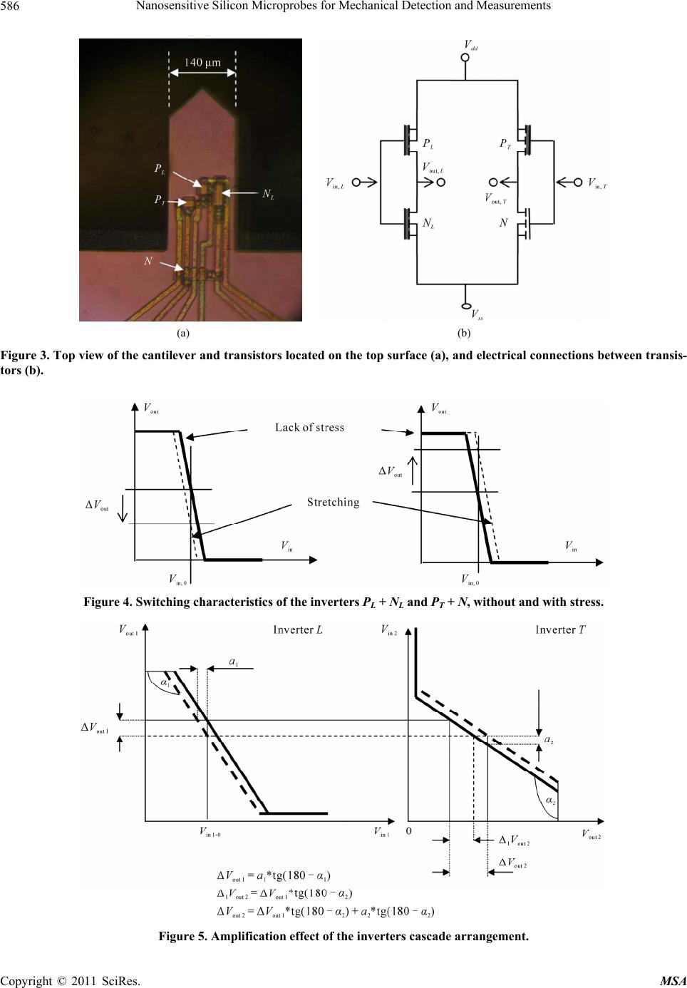 Nanosensitive Silicon Microprobes for Mechanical Detection and Measurements 586 (a) (b) Figure 3. Top view of the cantilever and transistors located on the top surface (a), and electrical connections between transis- tors (b). Figure 4. Switching characteristics of the inverters PL + NL and PT + N, without and with stress. Figure 5. Amplification effect of the inverters cascade arrangement. Copyright © 2011 SciRes. MSA  Nanosensitive Silicon Microprobes for Mechanical Detection and Measurements 587 assume, that a1 = a2 = 10 μV and typical slope of charac- teristic in the switching region is tg (180 – ) = 100. In such an assumptions output voltage of the single inverter will change by only 1 mV in comparison to the inverters cascade change by 1010 mV. 3.2. Microprobe with the Ring Oscillator Close-up view on the topography of four inverters on the cantilever is shown on Figure 6(a), and of the ring oscillator other parts on Figure 6(b), [12]. Inverters on the cantilever consist of n-type transistors, which were separated by the 80 μm wide area from the p-type transistors. There are four electrical terminals (bonding pads) of the ring oscillator - power (UDD), ground (GND), output (OUT) and control signals (Start/Stop). Simmulation of the ring oscillator performance was done with use of SPECTRE software. Mechanical stress in the silicon cantilever cause changes of the electrical carriers effective mobility and this mobility changes were applied for simulations. With no mechanical stress in the cantilever calculated oscillation time was TOSC = 141 ns. Assumed 10% reduction of the carrier mobility cause 4,3% increase of the oscillation time TOSC = 6 ns. 4. Technology Microprobe fabrication integrates CMOS with MEMS technologies. As an input substrates DSP silicon wafers with (100) crystal orientation, 4”-diameter, 400 m- thickness, n-type and resistivity 3 - 5 ·cm were used. Whole CMOS technological sequence was performed up to the bonding pads formation step. At this stage indi- vidual transistors have to pass electrical tests to enter MEMS processing - cantilever formation. “Relief” tech- nique (Figure 7) was applied. It consist of several di- electric/metal layers deposition/sputtering steps, photo- lithographies with double-side alignment and combina- tion of etching steps, both in chemical solutions and plasma reactors. Thickness of the cantilever is generally very important parameter for the microprobe mechanical performance—stiffness nad stress distribution. Relief technique may be applied up to 3 - 4 m range with satis- factory yield of properly done microprobes. Further re- duction of the cantilever thickness, as well as better con- trol of the cantilever thickness across the wafer and be- tween the wafers in the batch, may be obtained with use of SOI wafers. Whole technology consists of more than 100 steps, among of them 14 photolithography’s, as listed in Table 2. Gate oxide 65 nm thick was formed in standard diffu- sion furnace 1000˚C, [O2 + 5% HCl]. Transistor gate electrodes were madeup from the polysilicon layer 500 nm thick, doped with phosphorous in the diffusion furnace (a) (b) Figure 6. Details of the layout fragments which are respon- sible for detection (a) buffers and control circuitries (b). Copyright © 2011 SciRes. MSA  Nanosensitive Silicon Microprobes for Mechanical Detection and Measurements 588 (a) (b) (c) Figure 7. Schemes of the cantilever cross section illustrating relief technique, which was applied to form cantilevers of appropriate thickness. Table 2. Masks for photolithography. Mask no Mask symbol Description of content 1 ALIGN-F Front-side alignment signs 2 ALIGN-B Back-side alignment signs 3 WELL P-type well 4 LOCOS Field oxide 5 P-CHAN P-type channel stopper 6 N-CHAN N-type channel stopper 7 POLY Poly-Si 8 NPLUS N-type S/D 9 PPLUS P-type S/D 10 CONT Contact windows 11 METAL Metal 12 TK Bonding pads 13 MBM Membrane 14 CANTI Cantilever 960˚C [POCl3], U/I = 2.5 . Source and drain elec- trodes were doped by means of ion implantation: B, 50 keV, 5 × 10¹⁵ (p-type transistors) and P, 80 keV, 5 × 10¹⁵ (n-type transistors). Also p-type well regions were im- planted with the boron ions 120 keV, 3 × 10¹². Passive areas of the microprobes were covered by the LOCOS silicon dioxide layer 1.1 μm thick. Contact windows were opened twice – first time in the double layer Si3N4/ SiO2, and second time in the SiO2/BPSG/PSG sandwich of total thickness about 1 m. Metal bonding pads and conductive paths were formed with Al layer deposition and photolithography, and passivated by the double layer PSG/SiO2 deposition of total thickness 0.7 m, Figure 8. 5. Microprobe Computer Model and Simulation Stress distribution across the cantilever and deformation were simulated with use of the CoventorWare software, [http://www.coventor.com]. Layout and original techno- logical sequence were directly implemented to build the model of microprobe, with particular interest focused on the cantilever area containing MOS transistors. Figure 9(a) illustrates an example of the simulated stress com- ponent YY distribution over the upper cantilever surface. In the region, where the CMOS transistors were located, tensile stress gets maximum values. This stress concen- tration is highly desirable for the microprobe sensitivity improvement. It is supposedly the result of several pho- tolithography’s & etching steps of the CMOS technology – the total thickness of deposited layers in this region is much thinner, than the total thickness of layers over the surrounding, passive areas of the microprobe. On Figure 9(b) there is a graph of extracted data of the stress com- ponent YY across the cantilever thickness, taken from the region of the transistor gate. Arrows on the graph indi- cate on the stress characteristic position of consecutive layers. The most important point of this characteristic is the YY stress value just under the gate oxide - transistor channel. To optimize microprobe sensitivity the design- ers and technology leaders should consider proportion between the total thickness of the CMOS originated lay- ers and Si thickness of the cantilever. They should avoid the situation, when these thicknesses are equal or almost equal, which means that the MOS transistor channel is located on (or very close) to the neutral plane of cantile- ver, with no stress (resulting in sensitivity loss by the microprobe). 6. Measurements Testing station consisted of the stage with precise me- chanical control of the positioning piezoelectric trans- ducer tip XY, as well as electrically controlled tip motion in Z direction (cantilever tip deformation), microprobe chip clamping (all above mentioned elements closed in- side the Faraday cage) and electronic instruments applied for power supply, control and measurement (located out- side the Faraday cage), Figure 10. Piezoelectric trans- ducer applied for the tests alowed independent position- ing of the tip relatively to the microprobe cantilever, as well as enforcement of precise cantilever tip deflection Copyright © 2011 SciRes. MSA  Nanosensitive Silicon Microprobes for Mechanical Detection and Measurements589 Figure 8. SEM top view of the silicon cantilever 2.87 μm thick. (a) (b) Figure 9. Computer simulation of the stress ( YY) distribu- tion over the cantilever upper surface (a) and graph across the cantilever thickness in the region of the MOS transistor gate (b); simulations were done with force 0.1 G concen- trated at the cantilever tip, as well as with real layout and technology of the microprobe. Figure 10. System for microprobe testing station - view in- side the Faraday cage. (bending) – the range of cantilever tip movement in Z direction was from 0 to 90 μm with resolution 2 nm. 7. Results 7.1. Inverter Dependence between the inverter switching point and cantilever tip deflection was examined and in every case linear characteristics were obtained. As an example, typical electro-mechanical characteristic of CMOS in- verter (type L) is presented on Figure 11. On Figure 11 piezoelectric transducer tip initial move by the distance of 600 nm is equal to the separation be- tween transcucer tip and cantilever surface – there is no mechanical contact between them, no cantilever deflect- tion, no mechanical stress in silicon and this results in the constant value of the inverter switching point. Further transcucer tip movement down in Z direction bends the cantilever, introduces stress and causes shift of the in- verter switching point. One may determine linear part in that region of the characteristic. On Figure 12 there is comparison of extracted linear parts of the switching point characteristics for the T type and L type inverters. Sensitivities are –1.8 mV/nm and +1.2 mV/nm, which is Copyright © 2011 SciRes. MSA  Nanosensitive Silicon Microprobes for Mechanical Detection and Measurements Copyright © 2011 SciRes. MSA 590 0.0 0.5 1.0 1.5 2.0 2.5 3.0 3.5 0 200 400 600 80010001200140016001800 2000 Deflection [nm] V out (V) Linearity range Figure 11. Shift of the inverter type L switching point with the cantilever tip deflection. In the linear part of characteristic measured microprobe sensitivity was –2.6 mV/nm. Figure 13. Linear ranges of the inverter cascades charac- teristics in configuration T + L and L + T; sensitivity T + L was 43.7 mV/nm and L + T was 38.2 mV/nm. Figure 12. Comparison of extracted linear parts of charac- teristics Vout in function of the cantilever tip deflection for inverters T type and L type. slightly different when compared to the theoretical re- sults –2.5 mV/nm and 1.7 mV/nm for L-type and T-type inverters, respectively. 7.2. Cascade Electro-mechanical tests were also done for the micro- probes with CMOS inverters in cascade arrangement. Figure 13 ilustrates measured results of the highest sen- sitivities obtained in the batch. Sensitivity of the micro- probe with inverters in T + L configuration was 43.7 mV/nm and in L + T was 38.2 mV/nm. 7.3. Ring Oscillator Results obtained from measurements done with use of two selected microprobes - O2 of the highest sensitivity and O4 of the lowest sensitivity in the batch - are shown on Figure 14. Frequences of the ring oscillators without Figure 14. Frequency v. deflection characteristics obtained from measurements of microprobes O4 and O2. Sensitivi- ties are 8 Hz/nm (the highest in the batch) and 5 Hz/nm (the lowest in the batch).  Nanosensitive Silicon Microprobes for Mechanical Detection and Measurements591 any stress in the cantilever were 10.794 MHz and 10.854 MHz, respectively. These results are in reasonable agreement with the simulations. Under the stress frequencies of the ring oscillators linearly decreased, as was predicted from the SPECTRE simulation results. Sensitivity of the mi- croprobes were in the 5 - 8 Hz/nm range. The minimum one (5 Hz/nm) was obtained for the O2 microprobe, the maximum one (8 Hz/nm) was obtained for the O4 mi- croprobe. These results confirm, that silicon microprobes with the ring oscillators may be applied for the stress, force and deflection measurements in nano ranges, which is especially interesting for the interdisciplinary areas, like chemical and biochemical sensing, [13]. The most important obstacle in measurements hardware was elec- trical and mechanical noise. It was observed, that micro- probes with the ring oscillators has much higher potential in resolution limits than the testing station. 8. Conclusions Microprobes with the CMOS transistors connected into individual inverters reveal deflection sensitivities 1.2 - 1.8 mV/nm. Cascade arrangement of the inverters con- sisting of the CMOS transistors increase microprobe de- flection sensitivity to 40 mV/nm, which corresponds the force sensitivity 2.2 mV/nN. The ring oscillator ar- rangement of the microprobe gave deflection sensitivity in the range 5 - 8 Hz/nm. Measuremets of the resonant frequency changes seems to be advantageous over the analog voltage (or current) small signals. REFERENCES [1] J. Bryzek, K. Petersen, J. R. Mallon Jr., L. Christel and F. Pourahmadi, “Silicon Sensors and Microstructures,” Sili- con Sensors and Microstructures, Silicon Valey, 1993. [2] R. Linnemann, T. Gotszalk, I. W. Rangelow, P. Dumania and E. Oesterschultze, “Atomic Force Microscopy and Lateral Force Microscopy Using Piezoresistive Cantile- vers,” Journal of Vacuum Science & Technology B: Mi- croelectronics and Nanometer Structures, Vol. 14, No. 2, 1996, pp. 856-860. [3] J. Thaysen, A. Boisen, O. Hansen and S. Bouwstra, “Ato- mic Force Microscopy Probe with Piezoresistive Read- Out and Highly Symmetrical Wheatstone Bridge Arran- gement,” Sensors and Actuators, Vol. 83, No. 1-3, 2000, pp. 47-53. doi:10.1016/S0924-4247(00)00299-5 [4] S. P. Timoshenko, “History of Strength of Materials,” Dover Publications, New York, 1983. [5] G. L. Bir and G. E. Pikus, “Symmetry and Strain-Induced Effects in Semiconductors,” Wiley, New York, 1972. [6] Y. Kanda, “Piezoresistance Effect of Silicon,” Sensors and Actuators, Vol. 28, No. 2, 1991, pp. 83-91. doi:10.1016/0924-4247(91)85017-I [7] C. S. Smith, “Piezoresistance Effect in Germanium and Silicon,” Physical Review Letters, Vol. 94, No. 1, 1954, pp. 42-49. doi:10.1103/PhysRev.94.42 [8] S. M. Sze, “Semiconductor Sensors,” Wiley, New York, 1994. [9] C. Canall, C. Canali, G. Ferla, B. Morten and A. Taronif, “Piezoresistivity Effects in MOS-FET Useful for Pressure Transducers,” Journal of Physics D: Applied Physics, Vol. 12, No. 11, 1979, pp. 1973-1983. doi:10.1088/0022-3727/12/11/025 [10] P. Dumania, “System Designed to Detect Stress in Mi- cromechanical Silicon Structures,” Polish Patent Pending No. PL 361525 (A1), 7 February 2005. [11] P. Dumania, “Nanosensitive CMOS System for the Sili- con Microbeam Deformation Measurements,” Proceed- ings of 9th Scientific Conference Optoelectronic and Electronic Sensors COE 2006, Cracow, 19-22 June 2006, pp. 449-452. [12] P. Dumania, et al., “CMOS Ring Oscillator as a Detection Unit for Silicon Nanosensitive Microprobes,” Proceed- ings of 10th Scientific Conference Optoelectronic and Electronic Sensors COE 2008, Poznan, 2008, pp. 214- 216. [13] G. Shekhawat, S.-H. Tark and V. P. Dravid, “MOSFET- Embedded Microcantilevers for Measuring Deflection in Biomolecular Sensors,” Science, Vol. 311, No. 5767, 2006, pp. 1592-1595. doi:10.1126/science.1122588 Copyright © 2011 SciRes. MSA |