Journal of Electromagnetic Analysis and Applications
Vol.5 No.1(2013), Article ID:27314,9 pages DOI:10.4236/jemaa.2013.51005
Efficient Time-Domain Signal and Noise FET Models for Millimetre-Wave Applications
![]()
School of Electrical Engineering and Computer Science, University of Ottawa, Ottawa, Canada.
Email: sasad063@uottawa.ca, myagoub@uottawa.ca
Received October 10th, 2012; revised November 15th, 2012; accepted November 30th, 2012
Keywords: Distributed Model; FDTD; Noise Correlation Matrix; FET
ABSTRACT
Based on the active coupled line concept, a novel approach for efficient signal and noise modeling of millimeter-wave field-effect transistors is proposed. The distributed model considers the effect of wave propagation along the device electrodes, which can significantly affect the device performance especially in the millimetre-wave range. By solving the multi-conductor transmission line equations using the Finite-Difference Time-Domain technique, the proposed procedure can accurately determine the signal and noise performance of the transistor. In order to demonstrate the proposed FET model accuracy, a distributed low-noise amplifier was designed and tested. A model selection is often a trade-off between procedure complexity and response accuracy. Using the proposed distributed model versus the circuit-based model will allow increasing the model frequency range.
1. Introduction
Efficient Computer-Aided Design (CAD) of high-frequency systems is critically based on the performance of their internal component models. As the core of modern communication systems, active devices should be then carefully modeled for reliable system design. In high frequencies, when the device physical dimensions become comparable to the wavelength, the input active transmission line has a different reactance from the output transmission line [1,2], exhibiting different phase velocities for the input and output signals. Therefore, the phase cancellation due to the phase velocity mismatching will affect the device performance [3]. Thus, a full-wave timedomain analysis involving distributed elements should be considered. However, this type of analysis is highly time consuming [4-6], even if different simulation time reduction techniques have been already proposed [7]. As a result, semi-distributed models such as the slice model could be seen as a suitable alternative to overcome this limitation [8]. However, by increasing the frequency up to the millimetre-wave range, the slice model cannot precisely model the wave propagation effect and phase cancellation phenomena. Therefore, to achieve more accurate design in millimetre-wave applications, one needs to develop a more advanced distributed model.
In this paper, a distributed model is proposed [9]. It includes the effect of wave propagation along the electrodes more accurately than the semi distributed model although the CPU time of this model is a little higher than the slice model. Since a time domain analytical solution does not exist, a numerical approach was used. Among all the existing methods, the Finite-Difference Time-Domain method (FDTD) was retained as one of the most widely used in this area [10]. The proposed model was demonstrated through the design of a distributed amplifier.
2. Signal FET Modeling
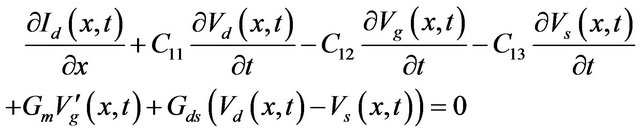
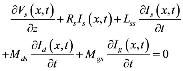
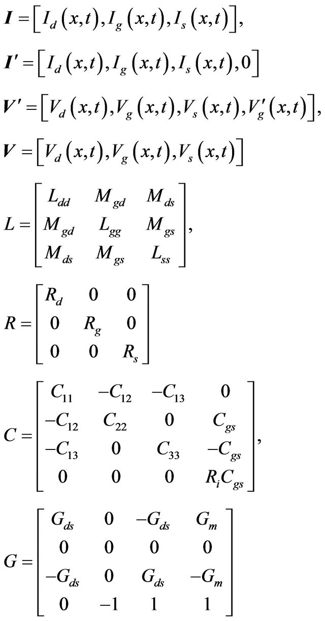
The proposed millimetre-wave Field Effect Transistor (FET) model is shown in Figure 1. It consists of three active coupled transmission lines (i.e., the three coupled electrodes of the device). As shown in this Figure, each elementary section Dx of the model can be represented by a 6-port equivalent circuit. This approach combines a conventional FET small-signal equivalent circuit model with a distributed circuit to account for the coupled transmission line effect of the electrode structure where all parameters are per unit length. With the condition Δx → 0, we obtain the following system of equations [11,12]:
 (1)
(1)
 (2)
(2)
 (3)
(3)
 (4)
(4)
 (5)
(5)
 (6)
(6)
with
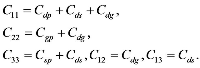
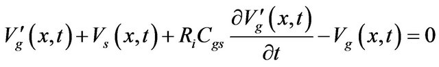
and where Vd, Vg, and Vs, are the drain, gate and source voltages, respectively, and  the voltage across gate-source capacitor. Id, Ig, and Is are the drain, gate and source currents, respectively. These variables are timedependant and function of the position x along the device width. Also, Mds, Mgd, and Mgs represent the mutual inductances between drain-source, gate-drain and gatesource, respectively; In the above system, we have an extra unknown parameter, i.e., the gate-source capacitance voltage
 . Therefore, the following equation should be included to complete the system of equations
 (7)
(7)
3. Noise FET Modeling
Similarly to the signal model proposed in the above section, a noise model can be developed based on the same concept, i.e., a set of transmission lines excited by noise equivalent sources distributed on the conductors, as shown in Figure 2. We thus have
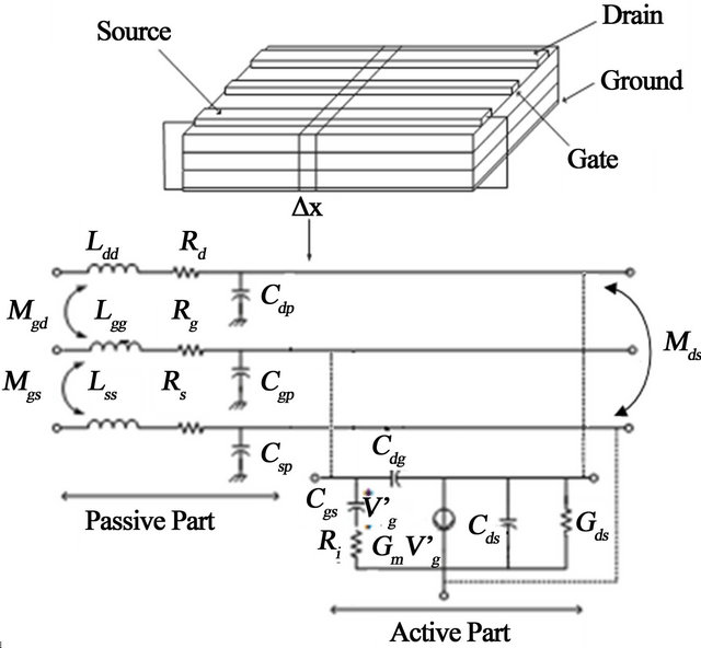
Figure 1. The different parts of a segment in the distributed model.
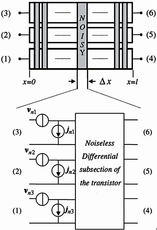
Figure 2. Noise-equivalent voltage and current sources.
 (8a)
(8a)
 (8b)
(8b)
where
Note that the vectors [vn] and [jn] in Figure 2 are the linear density of exciting voltage and current noise sources, respectively.
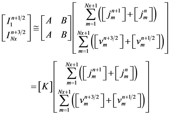
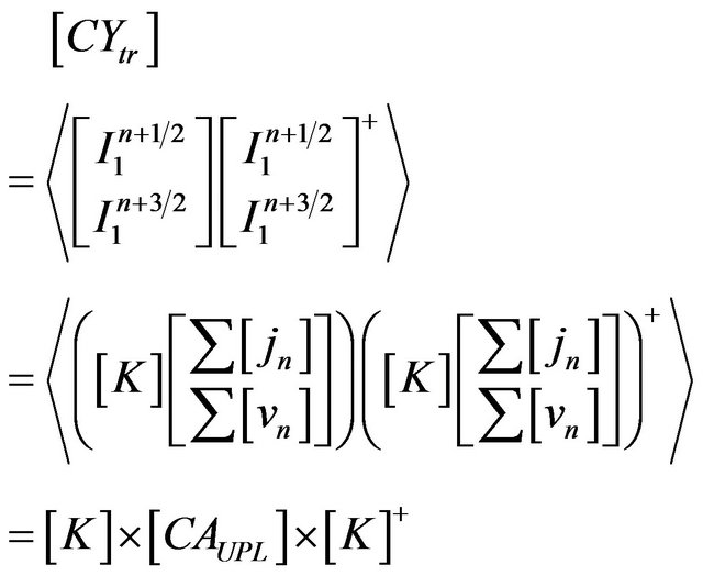
To evaluate the noise sources, we considered a noisy FET subsection with gate width Δx. Thus, the unit-perlength noise correlation matrix for chain representation of the transistor (CAUPL) can be deduced as [13]
 (9)
(9)
where < > denotes the ensemble average and + the transposed complex conjugate. According to the correlation matrix definition, we can calculate [vn] and [jn] knowing (CAUPL), to completely describe the proposed FET noise model. Indeed, by solving (9), the noise parameters of the transistor can be obtained.
Based on the transmission line circuit theory, the model impedance and admittance matrices can be expressed as
 (10)
(10)
where [R], [L], [C], and [G] refer to the matrix representation of the well-known distributed circuit parameters of a transmission line namely, the resistance R, the inductance L, the capacitance C, and the conductance G, respectively. [Ytr] is accounted for the active parallel sub-section of the model. By solving the second-order differential equations of the model, its voltage and current vectors can be written as [14]
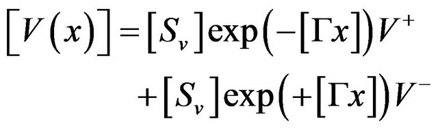 (11)
(11)
 (12)
(12)
where

and
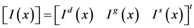
represent the voltage and current vectors at the transistor terminals, respectively (Here d, g, and s stand for drain, gate and source, respectively). The superscript “t” refers to the vector transpose. Let the elements of matrix [G] be the eigenvalues of [Z]·[Y] (or [Y]·[Z]) and the elements of matrices [Sv] and [Si] be the eigenvectors of [Z]·[Y] and [Y]·[Z], respectively [16]. By considering the boundary conditions of the six-port model, the unknown coefficients 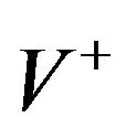 and
and  can be determined. Then, applying (11) and (12) for x = 0 and x = w, w being the gate width, the voltages and currents of each port can be obtained, leading to the 6*6 impedance
 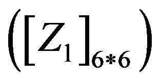 and admittance
  matrices of the model, which can be easily transformed to the scattering matrix form.
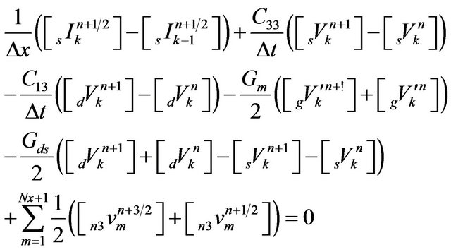
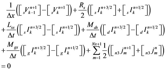
3.1. The FDTD Formulation
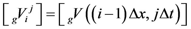
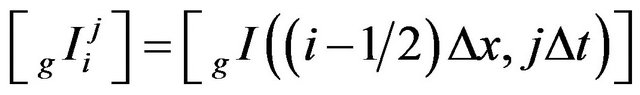
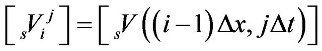
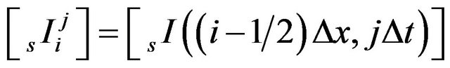
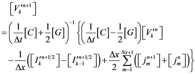
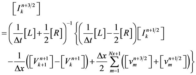
The FDTD technique was used to solve the above equations. Applications of the FDTD method to the full-wave solution of Maxwell’s equations have shown that accuracy and stability of the solution can be achieved if the electric and magnetic field solution points are chosen to alternate in space and be separated by one-half the position discretization, e.g., Δx/2, and to also be interlaced in time and separated by Δt/2 [15-16]. To incorporate these constraints into the FDTD solution of the transmission-line equations, we divided each line into Nx sections of length x, as shown in Figure 3. Similarly, we divided the total solution time into segments of length Δt. In order to insure the stability of the discretization process and to insure second-order accuracy, we interlaced the Nx + 1 voltage points,  and the Nx current points,
 . Each voltage and adjacent current solution points were separated by Δx/2. In addition, the time points were also interlaced, and each voltage time point and adjacent current time point were separated by Δt/2 [17,18]. Then, (8) can lead to

Figure 3. Relation between the spatial and temporal discretization to achieve second-order accuracy in the discretization of the derivatives.
 (13)
(13)
 (14)
(14)
 (15)
(15)
 (16)
(16)
 (17)
(17)
 (18)
(18)
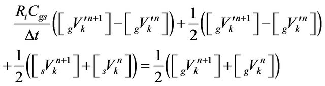
Applying the finite difference approximation to (7) gives
 (19)
(19)
with

and
 (20a)
(20a)
for the drain electrode
and
 (20b)
(20b)
for the gate electrode
and
 (20c)
(20c)
for the source electrodewhere k, m and n are integers. Solving these equations gives the required recursion relations
 (21)
(21)
 (22)
(22)
Superposing all the distributed noise sources is equivalent to a summation in (21) and (22) over the gate width for . Because of its simplicity, the leapfrog method was used to solve the above equations [13,14]. First the voltages along the line were solved for a fixed time using (21) then the currents were determined using (22). The solution starts with an initially relaxed line having zero voltage and current.
3.2. Transistor Noise Correlation Matrix
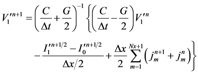
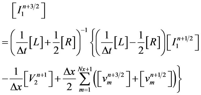
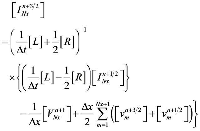
To find the noise correlation matrix for admittance representation of the transistor as a noisy six-port active network (as in Figure 2), the values of port currents should be determined when they are all assumed shortcircuited simultaneously. Equation (21) for k = 0 and k = Nx + 1 becomes
 (23)
(23)
 (24)
(24)
By considering Figure 3, this equation requires that we replace Δx by Δx/2 only for k = 1 and k = Nx+1.
In order to determine the transistor noise parameters, we set the input voltage source as zero (Vs = 0). Referring to Figure 4, we denoted the currents at the source point (x = 0) as I0 and at the load point (x = L) as INx+1. To determine the currents I1 and INx at short-circuited ports (x = 0 and x = L), we set V1 = VNx+1 = 0. The finite difference approximation of (23) for k = 1 and k = Nx can be then written as (25) and (26), respectively.
 (25)
(25)
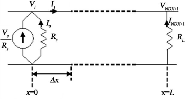
Figure 4. Voltage and current solution points. Spatial discretization of the line showing location of the interlaced points.
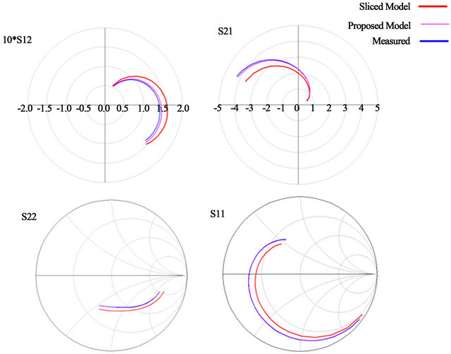
Figure 5. Comparison between S-parameters of NE710 for sliced, proposed distributed model and measurements.
 (26)
(26)
Finally, the currents of the short-circuited ports can be determined as
 (27)
(27)
with

The admittance noise correlation matrix of the six-port FET noise model is then equal to
 (28)
(28)
4. Numerical Results
The proposed approach was used to model a sub micrometer-gate FET transistor (NE710). The device has a 0.3 × 560 μm gate. The input and output nodes were connected to the beginning of the gate electrode and at the end of the drain electrode, respectively. The transistor was biased at Vds = 3 V and Ids = 10 mA. The obtained S-parameters of the transistor over a frequency range of 1-26GHz from the sliced model, the proposed fully distributed model and measurements are plotted in Figure 5.
As expected, our distributed model is more close to measurements than the slice model, especially at the upper part of the frequency spectrum, when the device physical dimensions are comparable to the wavelength. Figure 6 shows the noise figure obtained for three different sets of data.
To further prove the accuracy of the proposed wave approach in noise analysis, our results were successfully compared to measurements as well as to those obtained by the sliced model, highlighting the advantage of our model over this later (Figure 7). Thus, the proposed wave analysis can be applied for accurate noise analysis of FET circuits.
5. Amplifier Design and Analysis
To validate our proposed FET model, a three stage distributed FET amplifier was designed. In this work we considered a Pi-gate FET transistor suitable for low-noise applications. The topology of the gate and drain lines for transmission line modeling is shown in Figure 8 while the amplifier layout is shown in Figure 9.
The obtained power gain and minimum noise figure of the amplifier are shown in Figures 10 and 11, respecttively. As we observe there is good agreement between the proposed model and measurements as compared with the sliced model.
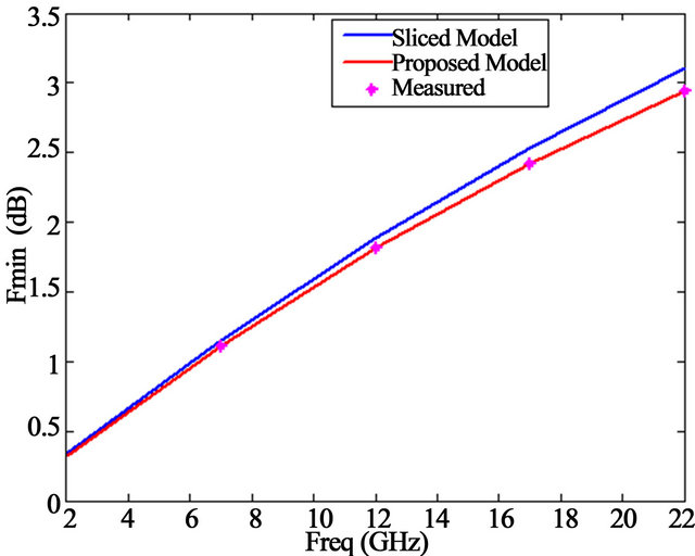
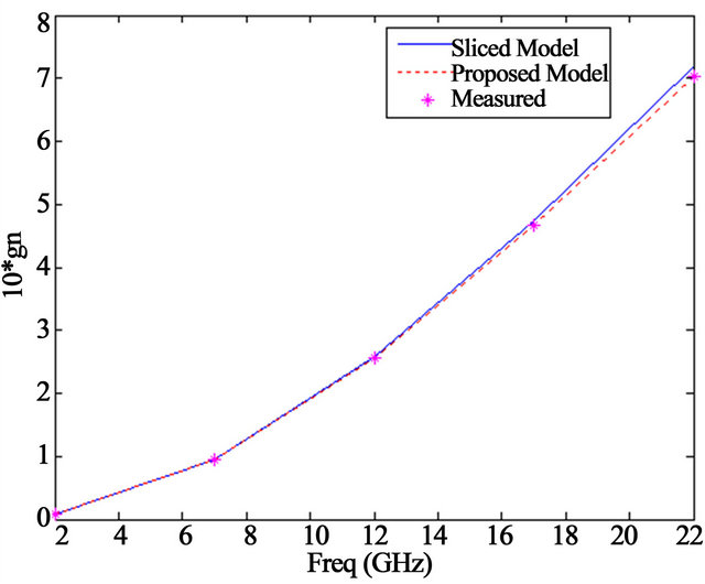
Figure 6. Comparison between normalized equivalent noise admittance and noise figure of FET for sliced, proposed distributed model and measurements.
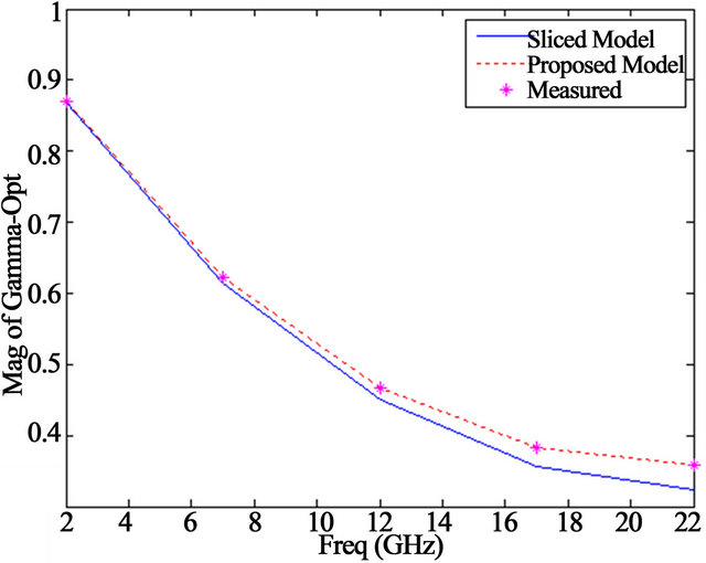

Figure 7. Comparison between the results of slice modeling, proposed model and measured values of amplitude and the phase of optimum reflection coefficient.
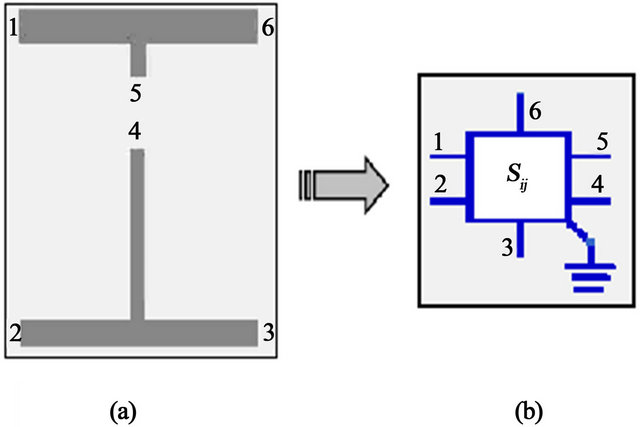
Figure 8. (a) Gate and drain lines topology; (b) Equivalent wave model.
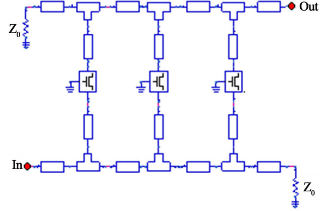
Figure 9. Designed three-stage distributed amplifier.
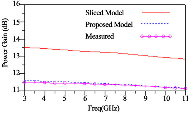
Figure 10. Power gain comparison for measured, proposed model and sliced model for distributed amplifier.

Figure 11. Minimum noise figure comparison for measured, proposed model and sliced model for distributed amplifier.
6. Conclusion
A new modeling approach for signal and noise analysis of high frequency transistors was presented. This method can accurately take into account the effect of wave propagation along the device electrodes. The promising model can be applied to solve issues related to simultaneous signal and noise analysis, as well as in modeling traveling wave FETs in which the gate width is much higher than that of a usual FET
REFERENCES
- J. Li, L.-X. Guo and H. Zeng, “FDTD Investigation on Bistatic Scattering from a Target above Two-Layered Rough Surfaces Using UPML Absorbing Condition,” Progress in Electromagnetics Research, Vol. 88, 2008, pp. 197-211. doi:10.2528/PIER08110102
- M. Y. Wang, et al., “FDTD Study on Wave Propagation in Layered Structures with Biaxial Anisotropic Metamaterials,” Progress in Electromagnetics Research, Vol. 8, 2008, pp. 253-265.
- R. Mirzavand, A. Abdipour, G. Moradi and M. Movahhedi, “Full-Wave Semiconductor Devices Simulation Using Adi-FDTD Method,” Progress in Electromagnetics Research, Vol. 11, 2010, pp. 191-202. doi:10.2528/PIERM10010604
- W. Heinrich, “Distributed Equivalent-Circuit Model for Traveling-Wave FET Design,” IEEE Transactions on Microwave Theory and Techniques, Vol. 35, No. 5, 1997, pp. 487-491. doi:10.1109/TMTT.1987.1133688
- S. Asadi and M. C. E. Yagoub, “Efficient Time-Domain Noise Modeling Approach for Millimeter-Wave FETs,” Progress in Electromagnetics Research, Vol. 107, 2010, pp. 129-146. doi:10.2528/PIER10042012
- S. Gaoua, M. C. E. Yagoub and F. A. Mohammadi, “CAD Tool for Efficient RF/Microwave Transistor Modeling and Circuit Design,” Analog Integrated Circuits and Signal Processing Journal, Vol. 63, No. 1, 2010, pp. 59-70.
- A. Abdipour and A. Pacaud, “Complete Sliced Model of Microwave FETs and Comparison with Lumped Model and Experimental Results,” IEEE Transactions on Microwave Theory and Techniques, Vol. 44, No. 1, 1996, pp. 4-9. doi:10.1109/22.481378
- S. M. S. Imtiaz and S. M. Ghazaly, “Global Modeling of Millimeter-Wave Circuits: Electromagnetic Simulation of Amplifiers,” IEEE Transactions on Microwave Theory and Techniques, Vol. 45, No. 12, 1996, pp. 2208-2216.
- A. Cidronali, G. Leuzzi, G. Manes and F. Giannini, “Physical/Electromagnetic pHEMT Modeling,” IEEE Transactions on Microwave Theory and Techniques, Vol. 51, No. 3, 2003, pp. 830-838. doi:10.1109/TMTT.2003.808580
- S. Goasguen, M. Tomeh and S. M. Ghazaly, “Electromagnetic and Semiconductor Device Simulation Using Interpolating Wavelets,” IEEE Transactions on Microwave Theory and Techniques, Vol. 49, No. 12, 2001, pp. 2258-2265. doi:10.1109/22.971608
- Y. A. Hussein and S. M. Ghazaly, “Modeling and Optimization of Microwave Devices and Circuits Using Genetic Algorithms,” IEEE Transactions on Microwave Theory and Techniques, Vol. 52, No. 1, 2004, pp. 329-336. doi:10.1109/TMTT.2003.820899
- M. Movahhedi and A. Abdipour, “Efficient Numerical Methods for Simulation of High-Frequency Active Devices,” IEEE Transactions on Microwave Theory and Techniques, Vol. 54, No. 6, 2006, pp. 2636-2645. doi:10.1109/TMTT.2006.872937
- M. W. Pospieszalski, “Modeling of Noise Parameters of MESFETs and MODFETs and Their Frequency and Temperature Dependence,” IEEE Transactions on Microwave Theory and Techniques, Vol. 37, No. 9, 1989, pp. 385- 388. doi:10.1109/22.32217
- Y. F. Wu, M. Moore, T. Wisleder, P. Chavarkar and P. Parikh, “Noise Characteristics of Field-Plated HEMTs,” International Journal of High Speed Electronics and Systems, Vol. 14, No. 3, 2004, pp. 192-194. doi:10.1142/S0129156404002880
- M. C. Maya, A. Lázaro and L. Pradell, “A Method for the Determination of a Distributed FET Noise Model Based on Matched-Source Noise-Figure Measurements,” Microwave and Technology Letter, Vol. 41, No. 3, 2004, pp. 221-225. doi:10.1002/mop.20099
- A. Tafove, “Computational Electrodynamics: The Finite Difference Time-Domain Method,” Artech House, London, 1996.
- J. A. Dobrowolski, “Introduction to Computer Methods for Microwave Circuit Analysis and Design,” Artech House, Boston, 1991.
- J. A. Dobrowolski, “Computer-Aided Analysis, Modeling and Design of Microwave Networks (Wave Approach),” Artech House, Boston, 1996.