Journal of Electromagnetic Analysis and Applications
Vol.4 No.7(2012), Article ID:21267,5 pages DOI:10.4236/jemaa.2012.47042
A Wearable Dual-Band Dielectric Patch Antenna for LTE and WLAN
![]()
1National Telecom Regulatory Authority, Cairo, Egypt; 2Faculty of Electronic Engineering, Menoufia University, Menouf, Egypt; 3RF/Microwave and Photonics Group, Department of ECE, University of Waterloo, Waterloo, Canada; 4Shobraa Faculty of Engineering, Benha University, Cairo, Egypt.
Email: m_soliman23@hotmail.com
Received May 2nd, 2012; revised June 1st, 2012; accepted June 12th, 2012
Keywords: U-Slotted Patch Antenna; MWCNT; Dielectric Antenna and ADS
ABSTRACT
In this paper, a dual-band microstrip patch array antenna for both the Multiple Input Multiple Output (MIMO) 4G Long-Term Evolution (LTE) and the Wireless Local Area Network (WLAN) systems is developed. Design simulation and optimization processes are carried out with the aid of the Advanced Design System (ADS) electromagnetic simulator that using the full-wave Method of Moment (MoM) numerical technique [1]. Rectangular microstrip patch antenna constructed from Multi-Walled Carbon Nanotubes (MWCNT) ink with electrical conductivity of 2.2 × 10⁴ S/m and relative permittivity of 5-j1 is used as the conductor patch [2]. The patch is deposited on Rogers substrate RT-Durid 5880 single substrate with (εr = 2.2) and thickness of 62 mil. U-shape slot is used to provide the dual-band. The proposed antenna operates at 3.5 GHz for LTE and 5 GHz for WLAN. The proposed antenna parameters are compared with published results of copper patch [3,4] for the same application. Great enhancement in antenna size, matching, and frequency band width are achieved for the proposed antenna at the expense of gain and antenna efficiency compared with copper one. The proposed MWCNT dielectric antenna size is 18.4 mm × 27 mm compared with size of 27 mm × 37 mm for copper one respectively. The gain is better than 7 dBi with antenna efficiency of 87.29% at 3.5 GHz for copper patch antenna and is better than 1.692 dBi with antenna efficiency of 27.05% at 3.5 GHz for MWCNT respectively.
1. Introduction
MIMO systems have been studied extensively during the recent years. It is clear from the theoretical point of view that the use of MIMO systems increases the capacity of transferred signal as compared to the use of Single Input Single Output (SISO) and Single Input Multiple Output (SIMO) systems. 4G handheld telephones, iphones, and other new compact cellular equipments recommend the use of small-scale, multi-band MIMO antennas. In this paper, we cover both the 4G LTE and the WLAN bands. It can be used in other MIMO antenna applications.
Rapid developments of wireless communications coupled with recent progress in material exploration results in a growing interest to apply nanostructure materials for microwave devices. The need for developing new materials that provide wireless devices with novel properties, in particular wearable microstrip antennas, is suitable for applications where regular conductors may fail such as mining, fire or chemical for biological degrading environments. Nanoscale materials are the most promising candidates since they have proven to provide new properties that were not possible for traditional bulk material. Electrically conductive ink based on nanoscale material is one such example. We have developed MWCNTs suspended in an adhesive solvent to create printable ink.
In this paper, we present a microstrip rectangular antenna constructed from MWCNT ink for wearable applications based on MoM numerical technique.
MWCNT dries quickly, adheres homogenously, and possess the characteristics of a good conductor at microwave frequencies. For the last several decades, conductive inks have stimulated the consideration and interest of many researchers due to their wide applications in microelectronics.
Some recent studies have used various composite materials as replacements for metals for antenna applications [5-8]. In [5], a conducting-polymer patch antenna is proposed. Silver nanoparticle ink [6] anmetallo-organic conductive ink [7] have been used to prepare a highlyconductive antenna. In [8].
Metals such as copper and aluminum are extensively used in aerospace and many other industrial applications. The high value of the conductivity of metal provides high shielding effectiveness and low loss in antennas and their associated ground planes. Some disadvantages of metals are their high weight, manufacturing cost and poor corrosion resistance. In some applications designers have sought a good alternative material to metals. For this purpose, many kinds of “composite” materials have been proposed [9-11]. Due to the low weight, ease of fabriccation, low cost, high stiffness, high thermal and electrical conductivity, carbon fiber composite (CFC) is one of the most desirable materials in the aerospace, electronic, and infrastructure industry [12].
MoM is one of the hardest to implement because it involves careful evaluation of Green’s functions and EM coupling integrals. Maxwell’s equations are transformed into integral equations yielding the coupling matrix equation of the structure via discretization. The advantage of this transform is that the current distributions on the metal surfaces emerge as the core unknowns. This is in contrast to other techniques which typically have the electric and/or magnetic fields (present everywhere in the solution space) as the core unknowns. Only the surfaces of the metals, where the currents flow, need to be taken into account in the meshing. Hence the number of unknowns (or the size of the matrix) is much smaller. This results in a very efficient simulation technique, which is able to handle very complex structures.
2. Single Element Design and Simulation
Figure 1 shows the optimize geometry of the rectangular copper patch antenna with dimensions of 27 mm × 37 mm and dimensions of 18.4 mm × 27 mm for MWCNT patch antenna respectively. More than 1.4% reduction in size is archived for the proposed MWCNT dielectric patch antenna over the copper one. Rogers substrate RTDurid 5880 single substrate with (εr = 2.2) and thickness of 62 mil. U-shape slot is used to provide the dual-band for both the LTE and WLAN applications. The MWCNT possess an electrical conductivity of 2.2 × 10⁴ S/m and a relative permittivity of 5-j1.
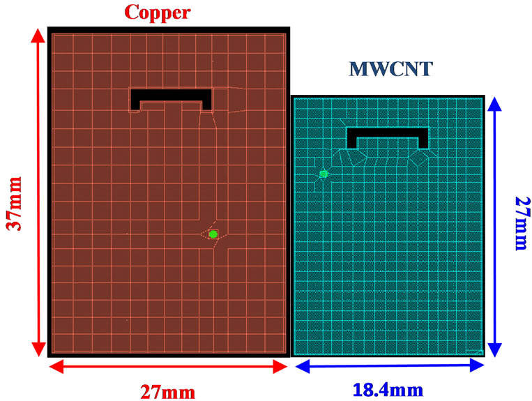
Figure 1. Geometry of copper and MWCNT patch antennas.
Figure 2 shows that the copper patch reflection coefficient S11 equals to –23.798 dB at 3.5 GHz with frequency bandwidth of 75 MHz for LTE, and equals to –20.871 dB with a frequency bandwidth of 80 MHz at 5 GHz for WLAN. The MWCNT patch reflection coefficient equals to –26.041 dB at 3.5 GHz with a frequency bandwidth of 150 MHz for LTE and equals to –27.941 dB with a frequency bandwidth of 350 MHz at 5 GHz for WLAN. The S11 values for the MWCNT antenna are better than the copper one, this ensures better matching. More than twice the bandwidth is archived for the proposed MWCNT dielectric patch antenna over the copper one.
Figure 3 shows the meandering of the surface current on the radiating U-slotted patch these results in an increase of the length of the equivalent surface current path.
Figures 4 and 5 show that the gain is better than 7 dBi with antenna efficiency of 87.29% at 3.5 GHz for copper patch antenna and is better than 1.692 dBi with antenna efficiency of 27.05% at 3.5 GHz for MWCNT patch antenna respectively. The reduction in antenna gain and efficiency for MWCNT dielectric patch antenna is expected compared to the copper one due to the reduced conductivity value of the MWCNT patch antenna and the corresponding reduction in conduction current value.
S11
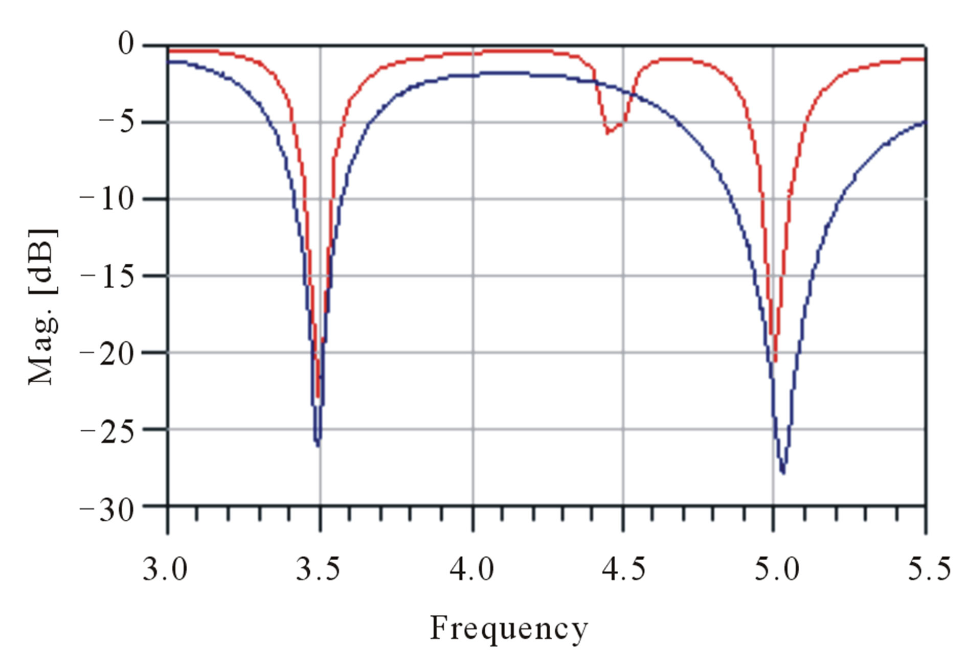
Figure 2. Reflection coefficient S11.
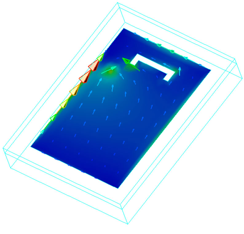
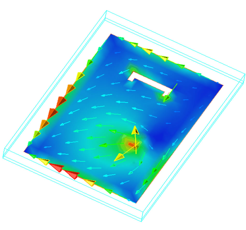
Figure 3. Meandering of surface current on the radiating surface.
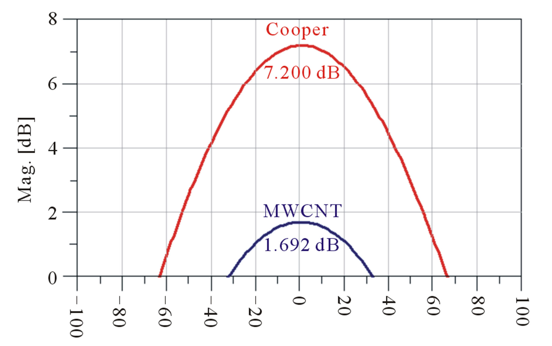
Figure 4. Gain 7.2 dBi for copper and 1.692 dBi for MWCNT.
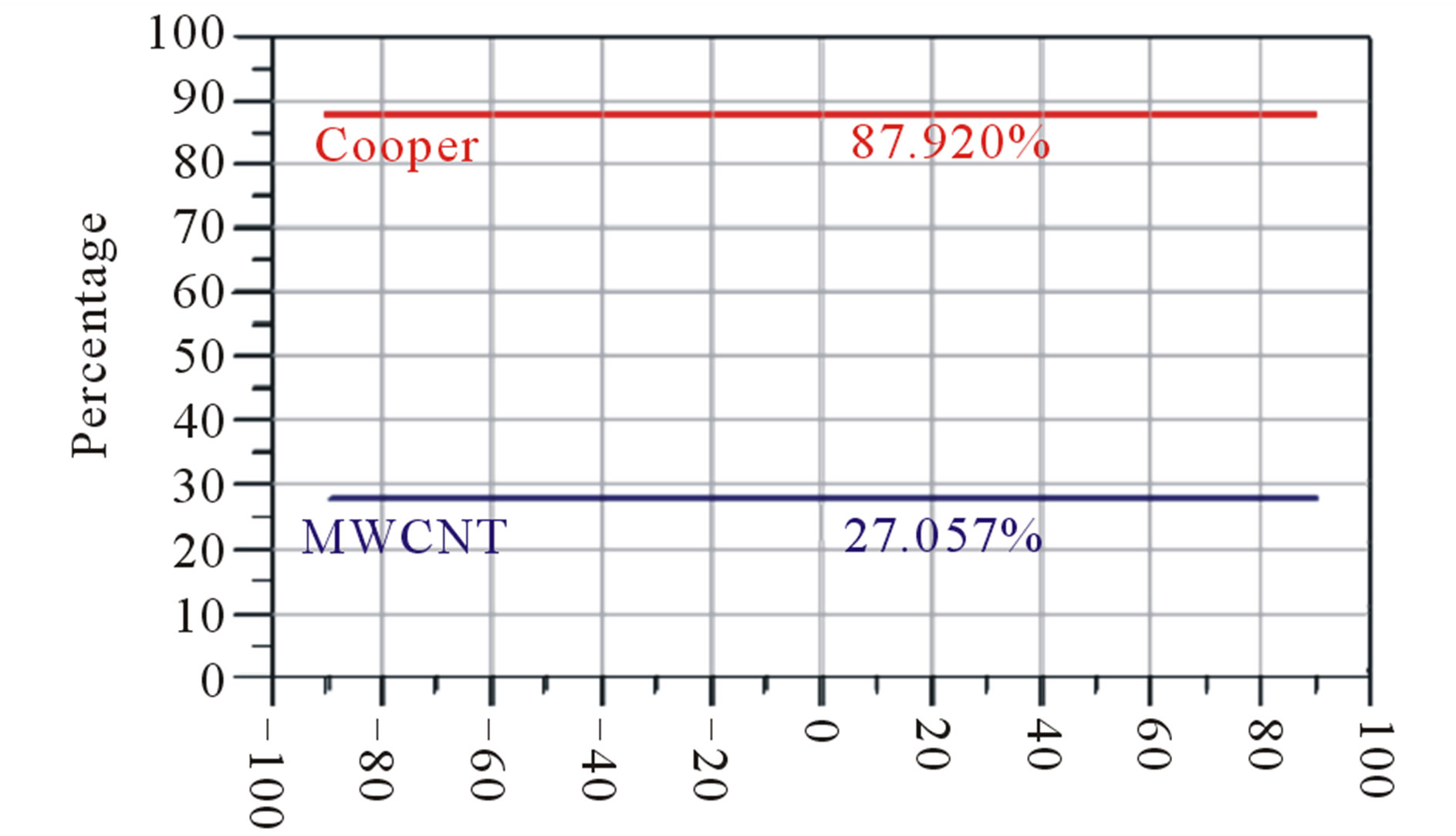
Figure 5. Antenna efficiency of 87.92% for copper patch antenna and 27.05% for MWCNT patch antenna.
3. 1 × 2 Array Antenna Design and Simulation
1 × 2 linear array antenna with element separation of λ/4 is showing in Figure 6 for both copper and MWCNT patches.
Figure 7 ensures good matching for the 1 × 2 array for both copper and MWCNT patches.
Figures 8 and 9 show that the gain is enhanced to be better than 7 dBi with antenna efficiency of 87.29% at 3.5 GHz for copper patch antenna and is better than 1.692 dBi with antenna efficiency of 27.05% at 3.5 GHz for WMCNT patch antenna.
4. 1 × 4 Array Antenna Design and Simulation
1 × 4 linear array antenna with element separation of λ/4 is showing in Figure 10 for both copper and MWCNT patches.
Figure 11 ensures good matching for the 1 × 4 array for both copper and MWCNT patches.
Figures 12 and 13 show that the gain is enhanced to be better than 7 dBi with antenna efficiency of 87.29% at 3.5 GHz for copper patch antenna and is better than 1.692 dBi with antenna efficiency of 27.05% at 3.5 GHz
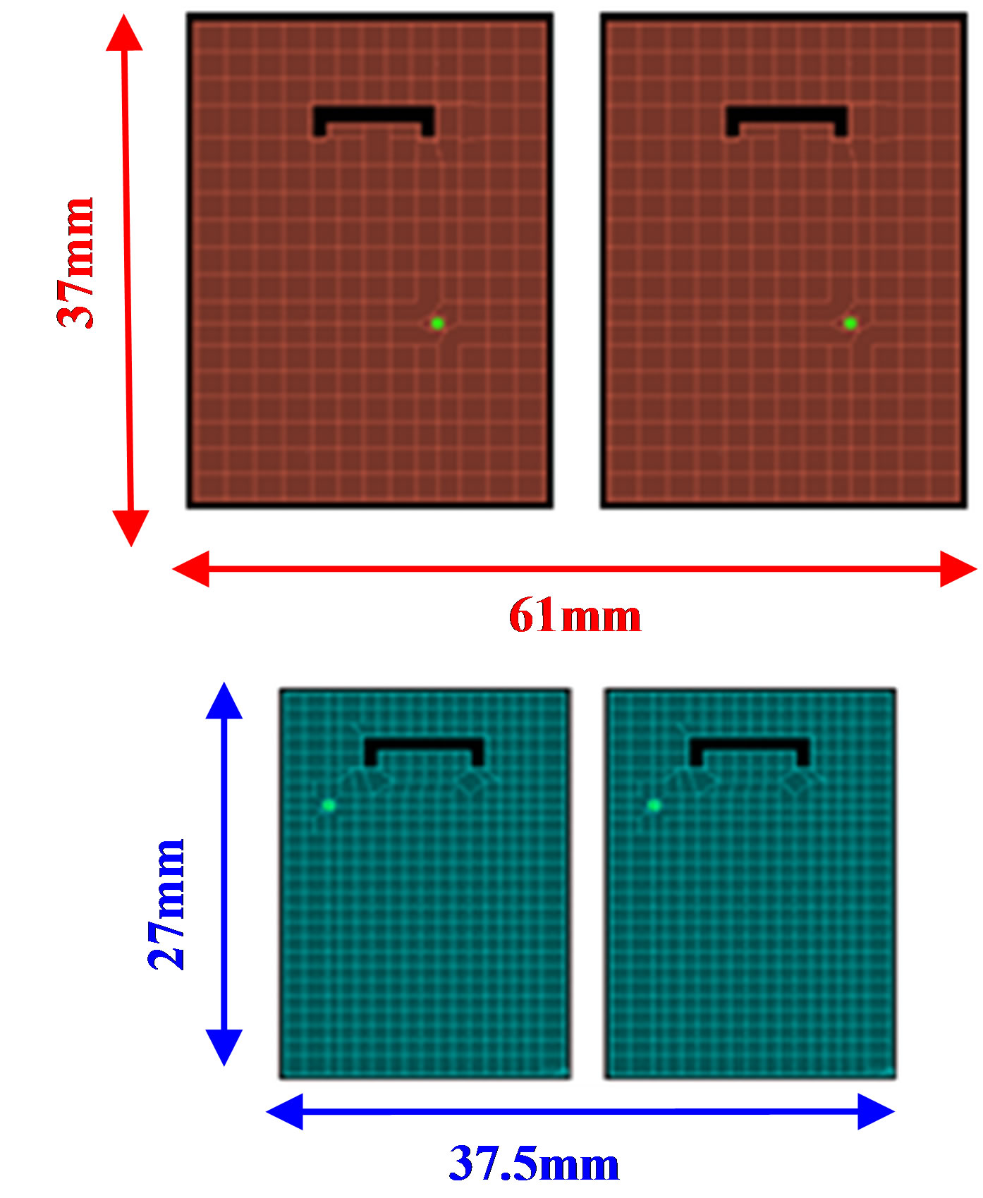
Figure 6. Geometry of 1 × 2 array antenna for copper and MWCNT patch antennas.
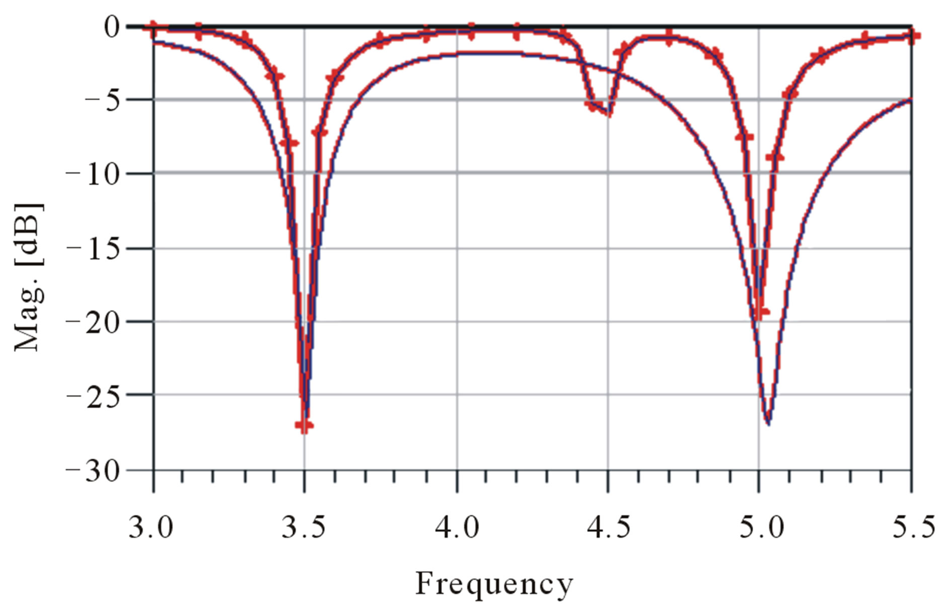
Figure 7. Reflection coefficient S11, S22 for copper and MWCNT.
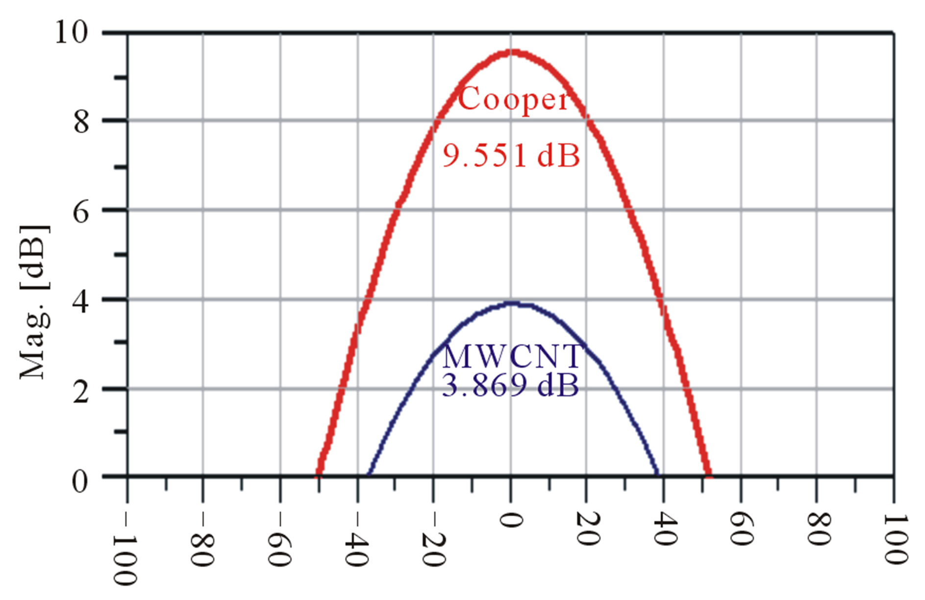
Figure 8. Gain 9.551 dBi for copper and 3.869 dBi for MWCNT.
for MWCNT patch antenna. Figure 14 shows the coupling coefficient among S12, S13, S14, S23 and S24 which ensures good results.
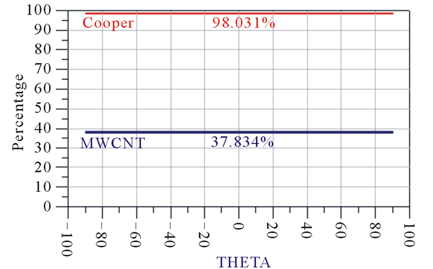
Figure 9. Antenna efficiency of 98.031% for copper and 37.834% for MWCNT.
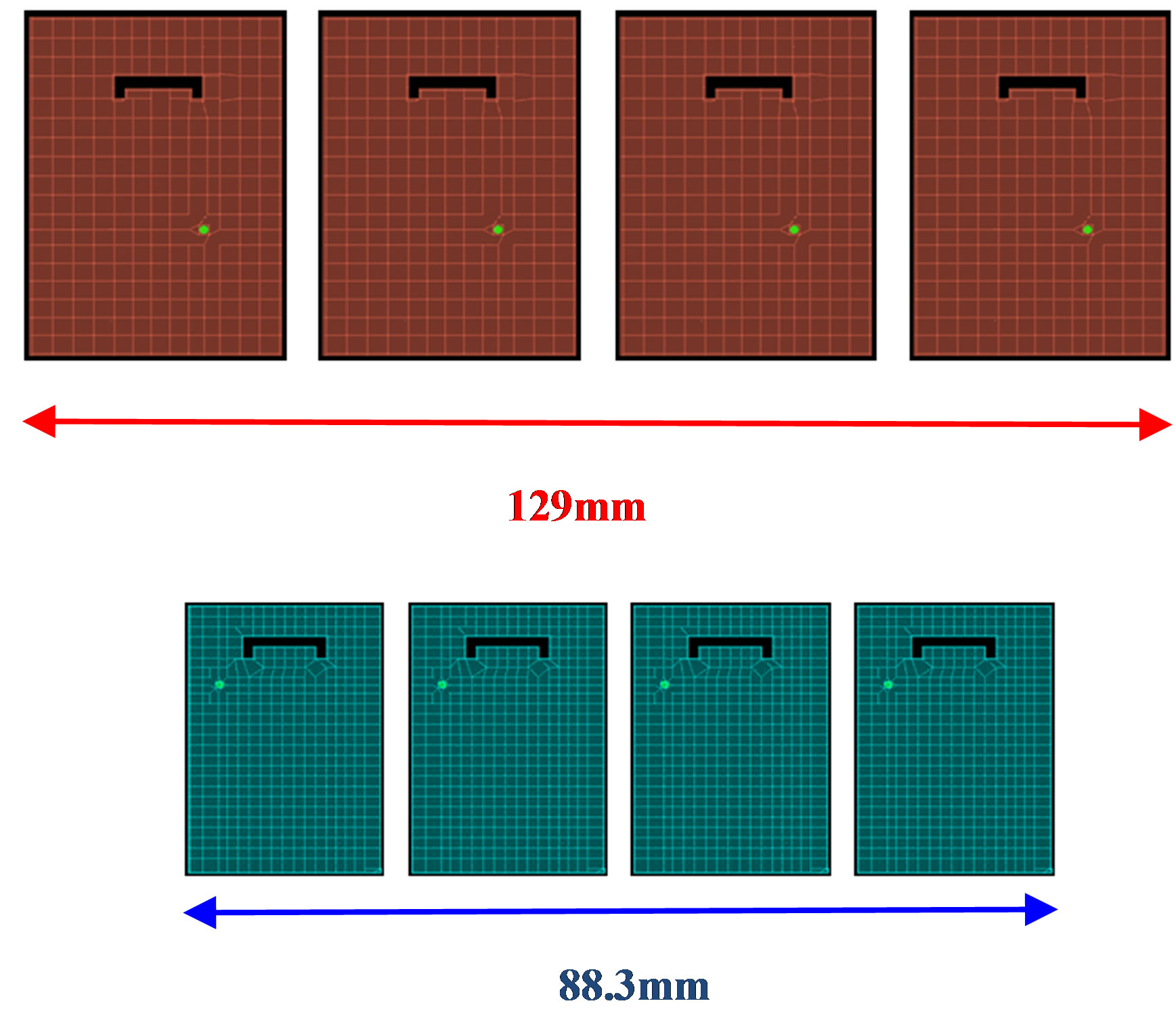
Figure 10. Geometry of 1 × 4 array antenna for copper and MWCNT patch antennas.
S11-S22-S33-S44
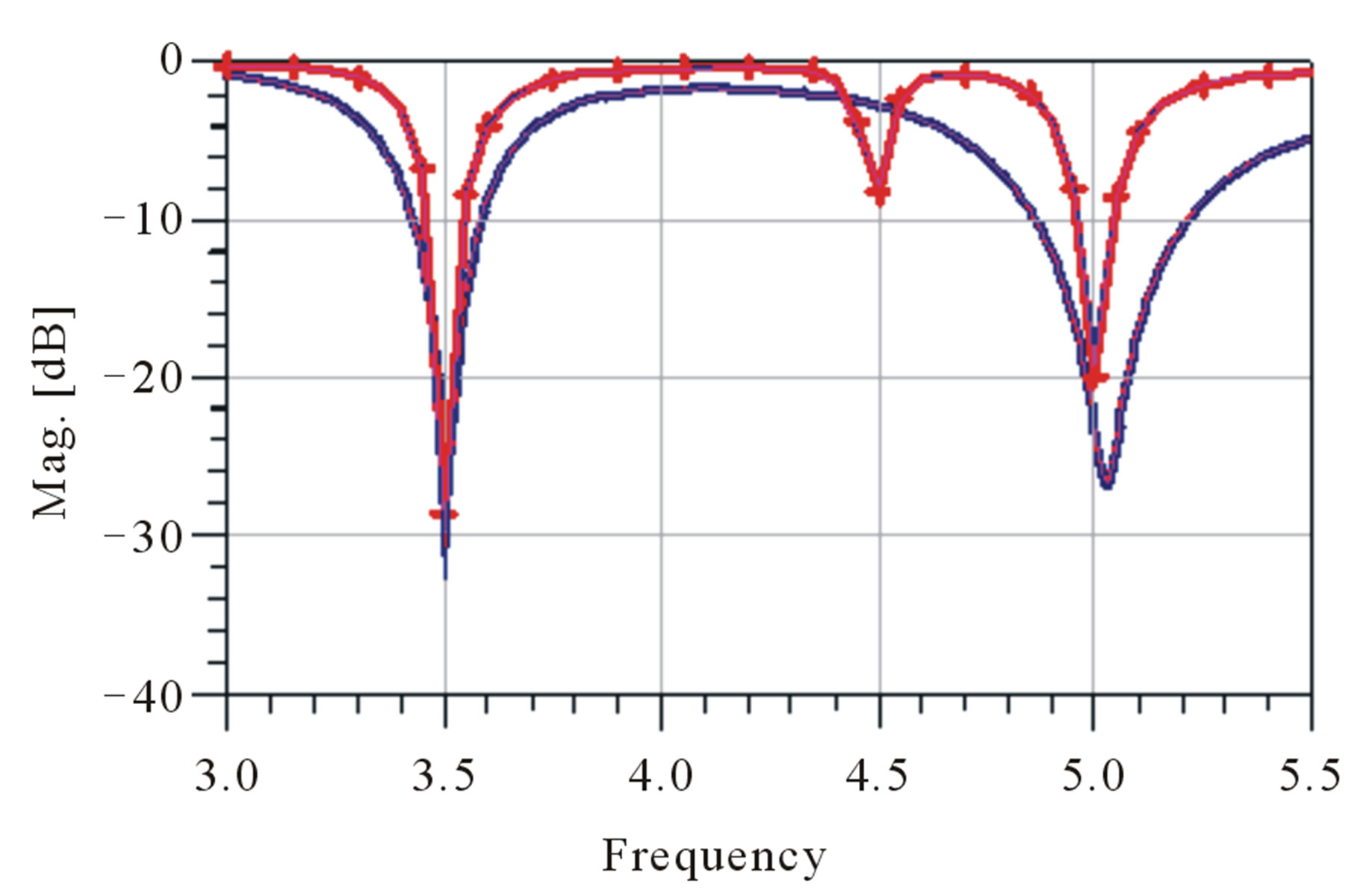
Figure 11. Reflection coefficient S11, S22, S33, S44.
5. Concolusion
Dual-band dielectric patch antenna for both the MIMO 4G Long-Term Evolution (LTE) and the Wireless Local Area Network (WLAN) systems is developed. The patch antenna is constructed from Multi-Walled Carbon Nanotubes (MWCNT) ink with electrical conductivity of 2.2 ×
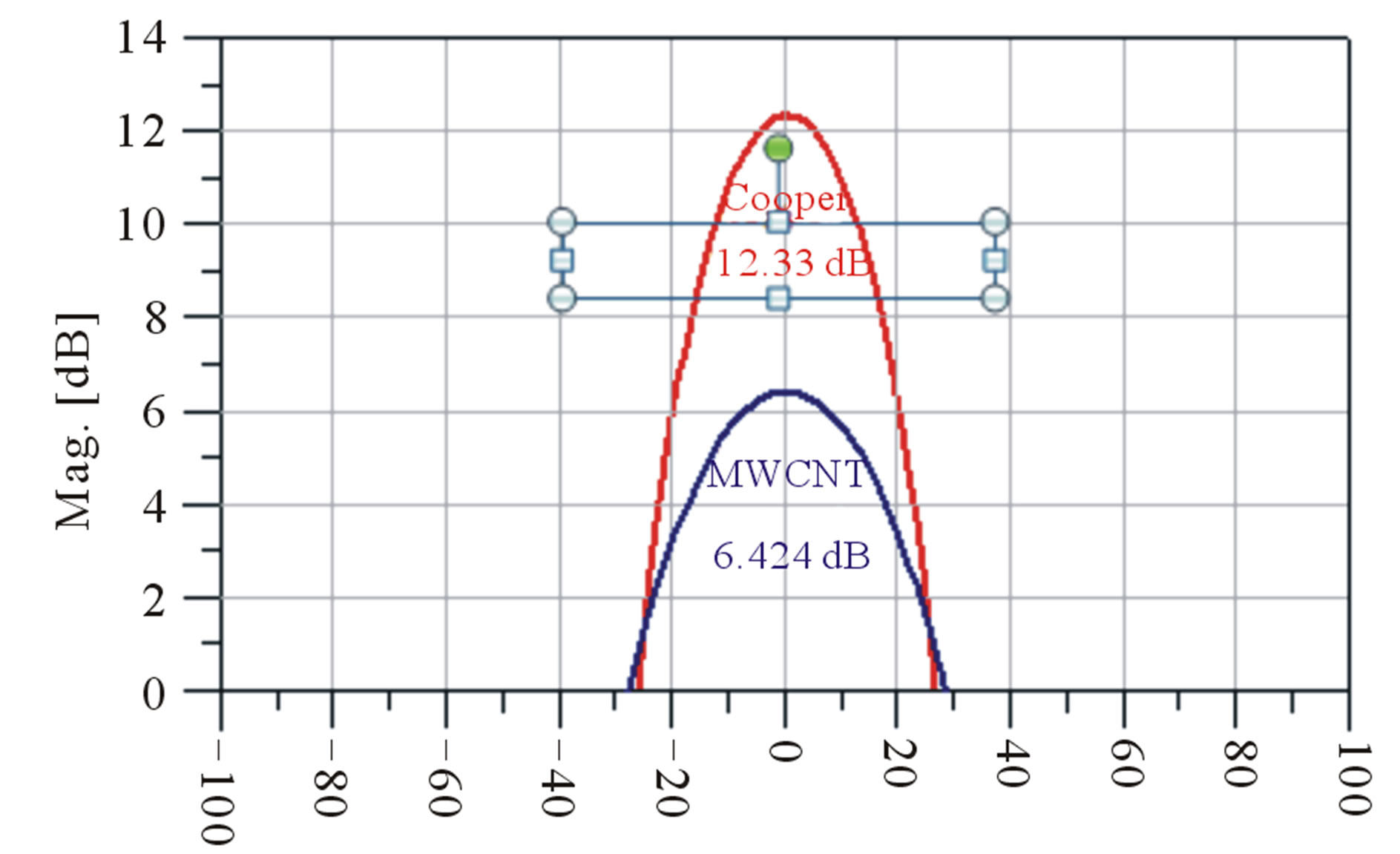
Figure 12. Gain 12.33 dBi for copper and 6.424 dBi for MWCNT.
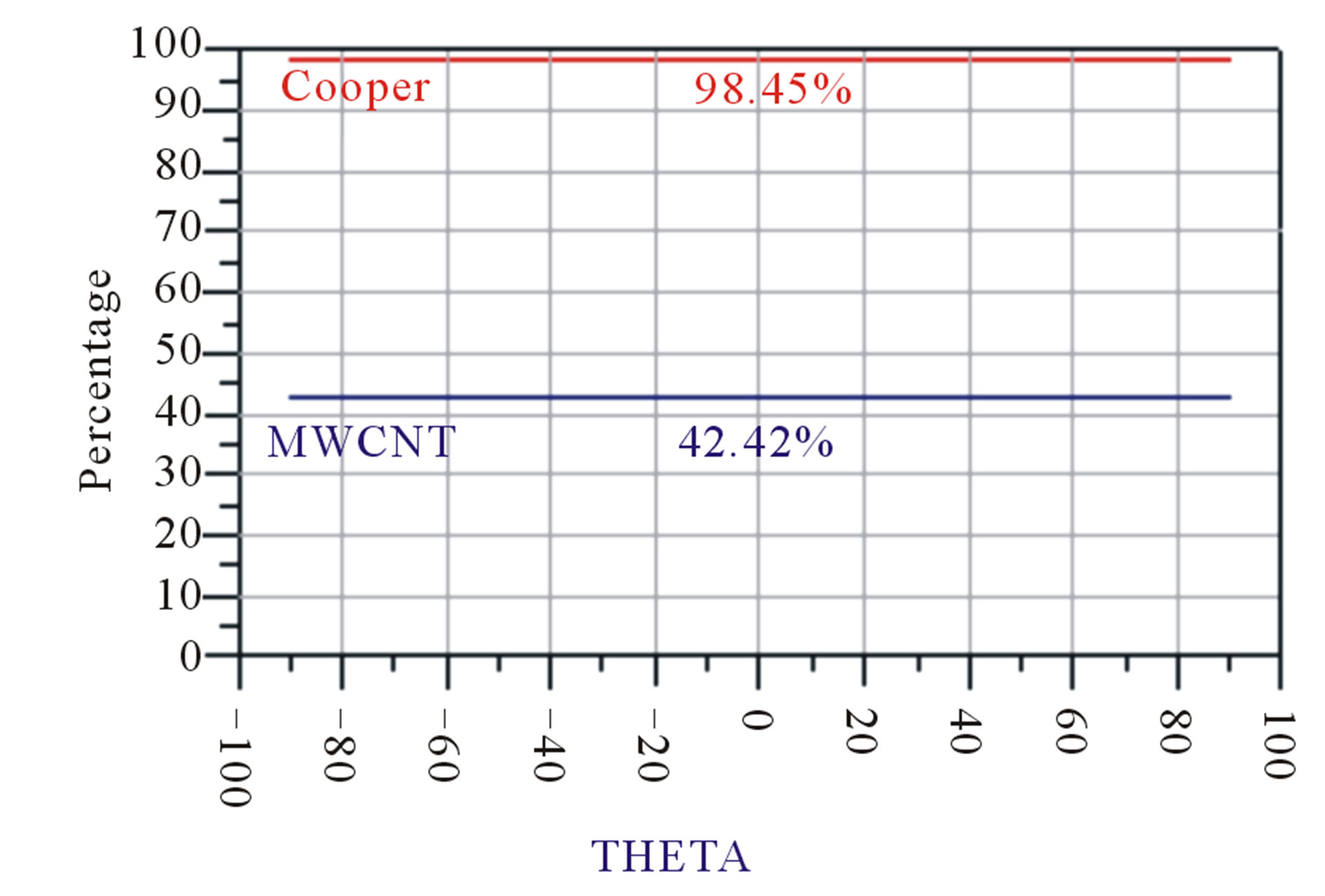
Figure 13. Antenna efficiency of 98.45% for copper and 42.42% for MWCNT.
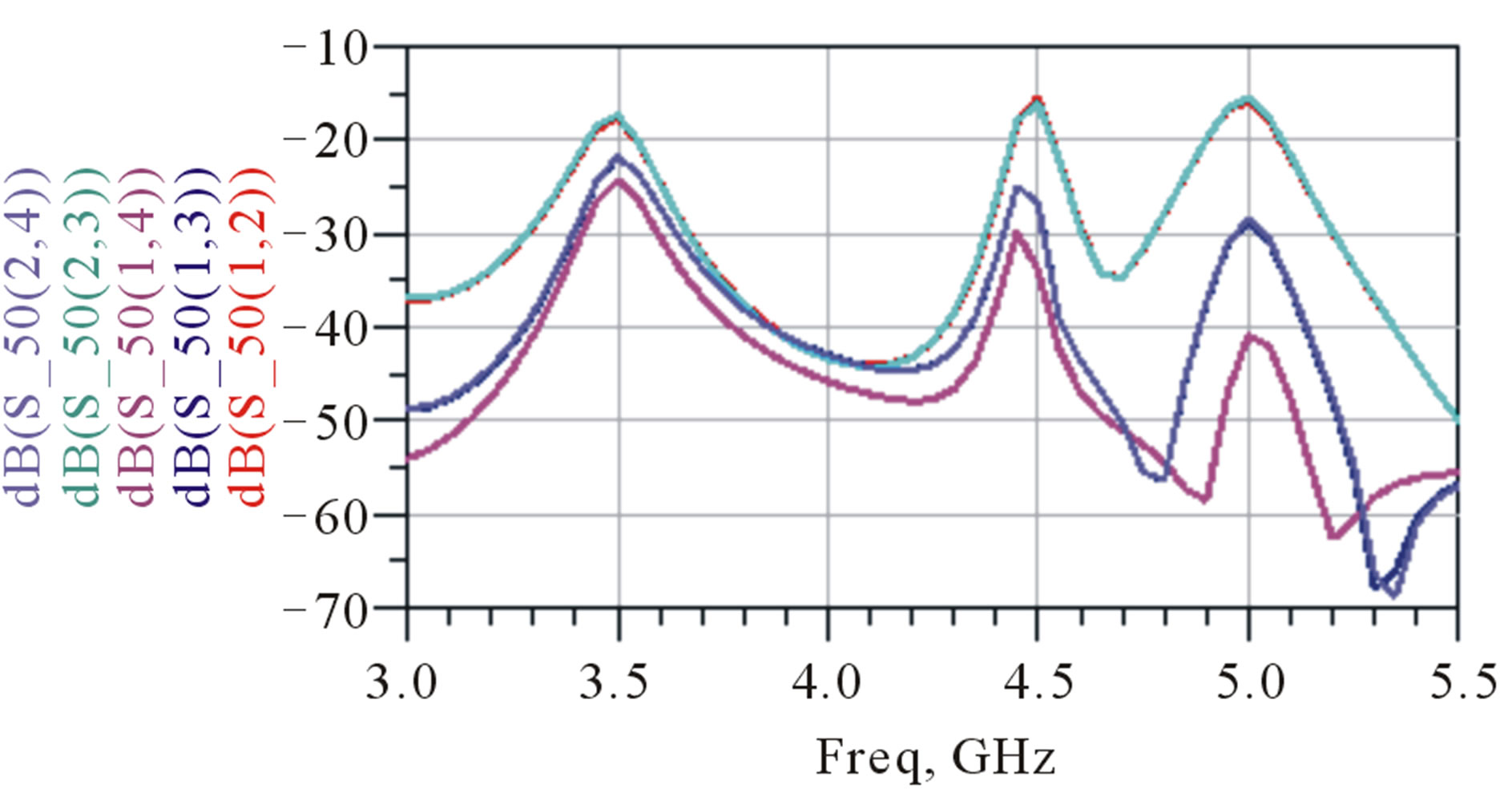
Figure 14. Coupling coefficient for S12, S13, S14, S23, S24.
104 S/m and relative permittivity of 5-j1. Design simulation and optimization processes are carried out using ADS simulator by MoM numerical technique. The patch is deposited on Rogers substrate RT-Duroid 5880 single substrate with dielectric constant εr = 2.2 and thickness of 62 mil. Optimized U-shape slot is used to provide the dual-band. The proposed antenna operates at 3.5 GHz for LTE and 5 GHz for WLAN systems. The proposed antenna simulation results are compared with published results from the same authors, with copper patch, for the same application. The proposed MWCNT dielectric antenna shows more than 1.4% reduction in size, better values of S11 parameter that ensures better matching, and more than twice the frequency bandwidth compared to the copper one. Reduction in antenna gain and efficiency compared to the copper one is expected due to the reduction in metal conductivity and conduction current values. Linear sub-arrays with dimensions of 1 × 2 and 1 × 4 of the proposed MWCNT dielectric antenna are designed and optimized. The proposed array antenna is suitable for MIMO LTE and WLAN applications.
REFERENCES
- Agilent Technologies Advanced Design System, ADS 2008 Momentum Software Manual, Agilent Technologies, Palo Alto, 2008.
- T. A. Elwi, D. G. Rucker, H. M. Al-Rizzo, H. R. Khaleel, E. Dervishi and A. S. Biris, “A Dual-Frequency Wearable MWCNT Ink-Based Spiral Microstrip Antenna,” NSTINanotechology, Vol. 1, 2010, pp. 266-269.
- M. Ali Soliman, W. Swelam, A. Gomaa and T. E. Taha, “Compact Dual-Band Microstrip Patch Array Antenna for MIMO 4G Communication Systems,” In the Proceeding of the 2010 IEEE Antennas & Propagation Symposium, (IEEE AP-S/URSI 2010), Toronto, 11-17 July 2010, pp. 1-4.
- M. A. Soliman, W. Swelam, A. Gomaa and T. E. Taha, “Compact Dual-Band Microstrip Patch Array Antenna for MIMO 4G LTE and WLAN Systems,” In the Proceeding of 7th International Conference on Electric Engineering (2010 ICEENG-7), during the 5th International Scientific Conference of the Military Technical College (ISCMTC-5), Cairo, 11-17 July 2010, pp. 1-4.
- D. D. L. Chung, “Review Electrical Applications of Carbon Materials,” Journal of Materials Science, Vol. 39, No. 8, 2004, pp. 2645-2661. doi:10.1023/B:JMSC.0000021439.18202.ea
- H. Rmili, J.-L. Miane, H. Zangar and T. Olinga, “Design of Microstrip-Fed Proximity-Coupled Conducting Polymer Patch Antenna,” Microwave and Optical Technology Letters, Vol. 48, No. 4, 2006, pp. 655-660. doi:10.1002/mop.21435
- L. Yang, A. Rida, R. Vyas and M. M. Tentzeris, “RFID Tag and RF Structures on a Paper Substrate Using InkJet-Printing Technology,” IEEE Transactions on Microwave Theory and Techniques, Vol. 55, No. 12, 2007, pp. 2894-2901. doi:10.1109/TMTT.2007.909886
- S. Ludmerer, “Conductive Inks for RFID Antenna: The Low Cost High Speed Route to RFID Labels,” Parelec Inc., Princeton.
- D. J. De Renzo, “Advanced Composite Materials Products and Manufacturers,” William Andrew, Norwich, 1988.
- S. V. Hoa, “Principles of the Manufacturing of Composite Materials,” DEStech Publications Inc., Lancaste, 2009.
- D. Gay, S. V. Hoa and S. W. Tsai. “Composite Materials: Design and Applications,” CRC Press, Boca Raton, 2003.
- A. Mehdipour, A. R. Sebak, C. W. Trueman, I. D. Rosca and S. V. Hoa, “Conductive Carbon Fiber Composite Materials for Antenna and Microwave Applications,” Faculty of Engineering/Cairo University, Cairo, 10-12 April 2012, pp. 1-8.