Journal of Electromagnetic Analysis and Applications
Vol.4 No.2(2012), Article ID:17672,11 pages DOI:10.4236/jemaa.2012.42011
Characterization of Shielding Efficiency for Power Electronics Frequency Domain
![]()
1Ampère Laboratory, University of Lyon, Lyon, France; 2Plastic Omnium, Auto Exterior, Sigmatech, Lyon, France.
Email: christian.vollaire@ec-lyon.fr
Received December 14th, 2011; revised January 15th, 2012; accepted January 24th, 2012
Keywords: Electromagnetic Shielding; Power Electronic; Converters
ABSTRACT
Today, new applications of power electronics systems appear in many domains like transport: more electric aircrafts or electric cars. In order to combine power and electronic systems in the same environment or to take into account normative constraints in term of electromagnetic field exposure for humans, electromagnetic compatibility (EMC) has to be integrated early in the design flow of the complete system (aircraft or car). The shielding is one of the most used solutions to avoid unwanted couplings between power systems and their environment. This paper presents a new experimental solution to determine the shielding efficiency of new material (composite material or association of different materials) in the frequency range of power electronic systems.
1. Introduction
Today new applications of power electronics systems appear in many domains like transport: more electric aircrafts or electric cars. In order to combine power and electronic systems in the same environment or to take into account normative constraints in term of electromagnetic field exposure for humans, electromagnetic compatibility (EMC) has to be integrated early in the design flow of the complete system (aircraft or car). The shielding is one of the most used solutions to avoid unwanted couplings between power systems and their environment. However, engineers have to identify the source of disturbance, its geometry and have to define the EMC constraints (for example the magnetic field at 8 cm in front of the converter [1]): what attenuation, what shielding in which material? Moreover, the solution must also satisfy others constraints like cost, weight, strength…
The sizing of a required shielding efficiency can be done analytically [2] in restricted cases: high frequency, far field and plane wave, 1D, homogenous, isotropic and single layer. The electromagnetic properties of the materials used have to be known. In the domain of power electronics, shielding must mitigate near fields coming from magnetic sources (strong currents with high variations) in the frequency range starting from a few kHz (chopping frequency) to 50 MHz (limit of the radiated emissions of a classical power electronics converter). In this specific case, analytical way is too limited to answer the industrial problematic.
Also, numerical analysis can be done to size a shielding in the frequency range of interest and for magnetic sources. However, a 3D Finite Element (FE) modeling is impossible to solve because of the number of unknowns due to the required mesh into the shielding to take into account the skin effect. A 2D approach is a good compromise between the number of unknowns and the reality of the modeled system. The only problem is then to know the properties of the materials used to inquire the numerical model. When new generations of materials are used (composite with inclusion of conducting nano material for example) a characterization phase is required to extract equivalent properties (permeability µ, conductiveity σ and permittivity ε).
For the frequency range of interest of power electronics devices (10 kHz to 50 MHz), there is no specific standard of experimental measurements to determine shielding efficiency [3-6]. So, a specific test bench has been developed to estimate the shielding efficiency in the context of power electronics.
This article describes the whole developed approach to solve the problematic of shielding in power electronics applications. First the analytical possibilities of sizing of shielding are described. This allows to have a canonical problem to validate the others approaches. Then, a 2D numerical modeling of shielding is described and a study of sensitivity of the size of the shielding under test compared to the diameter of the antennas is proposed. Finally, the sizing of the test bench is described; comparisons between analytical, 2D numerical and measurements results are made on different prototypes. New generation of materials (composite) and new associations of classical materials are then tested.
2. Context
In aeronautics, EMC problems are extremely important for the new generation “more electric” airplane, because the pneumatic and hydraulic actuators will be replaced by electrical ones (steering deflection, braking systems, landing gear…) in order to reduce the costs as well as the weight of the embedded systems. The use of electric materials in these systems, which have to take into account the constraints of aeronautical environments: vibrations, temperature, weight…, imposes reliability constraints and very strong restrictions in terms of EMC. Radiated emissions produced by such systems could create malfunctions in sensitive avionic surrounding equipments, in particular the embedded electronics.
In ground transport domain, two factors have given rise to new EMC problems: X-by-wire (drive-by-wire, fly-by-wire [7], break-by-wire [8] …) for sensitive and critical low level systems and hybrid or full electrical propulsion. Moreover, automotive manufacturers are concerned by constraints concerning the exposure of humans to electromagnetic fields.
To ensure a good functioning of critical low level systems and the security of persons near power electronics converters, normative constraints are imposed to manufacturers of systems or of vehicles [9]. These constraints can be “added” (i.e. take the maximum constraint for each frequency) giving specifications to meet. Starting from this specification (a maximum value of magnetic and/or electric field at a given place) and from the description of the electromagnetic source (geometry and electrical functioning) the shielding efficiency to meet can be expressed versus the frequency. Figure 1 shows an example of specification in term of shielding efficiency in the automotive domain. The H Field limit is specified in the interior of the vehicle in order to protect passengers and electronic equipments.
3. Analytical Sizing
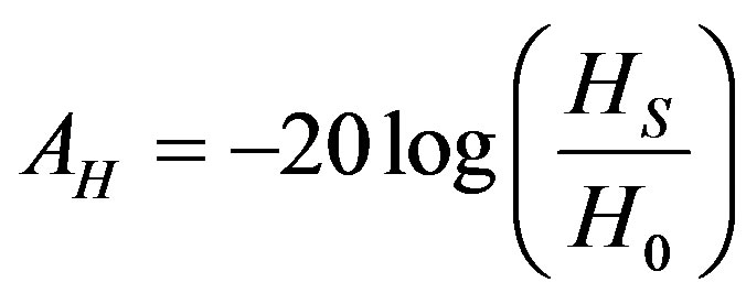
The shielding efficiency is evaluated by the attenuation in dB. In this study, the attenuation is defined by the ratio of the field at a place inside an enclosed shielded room (noted s) divided by the field at the same place but without the shielded room (noted 0). This ratio can be calculated with the modulus of the global field or for a given spatial component. The attenuation can be defined in terms of electric or magnetic field (1, 2).
 (1)
(1)
 (2)
(2)
In this study, the distance between the source of perturbation and the observation point, the maximal frequency of interest and the nature of the source (strong current values with strong variations) lead to consider magnetic sources in a near field configuration. So, the H field and the AH attenuation will be considered for the entire study.
In [2] authors develop analytical formalism with some restrictions ( in which ω is the pulsation of the
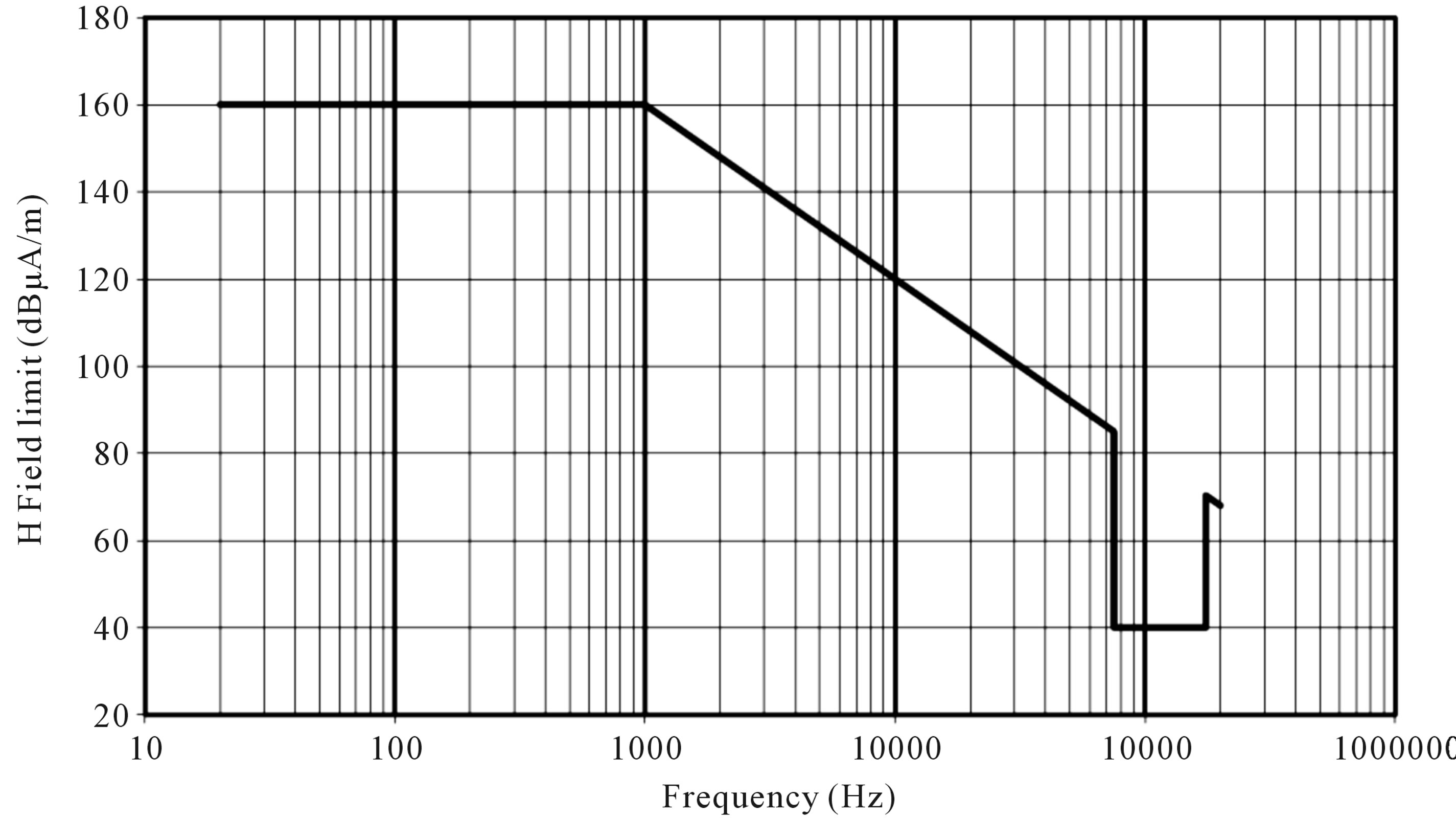
Figure 1. Example of a specification concerning the H field limit in the interior of the vehicle.
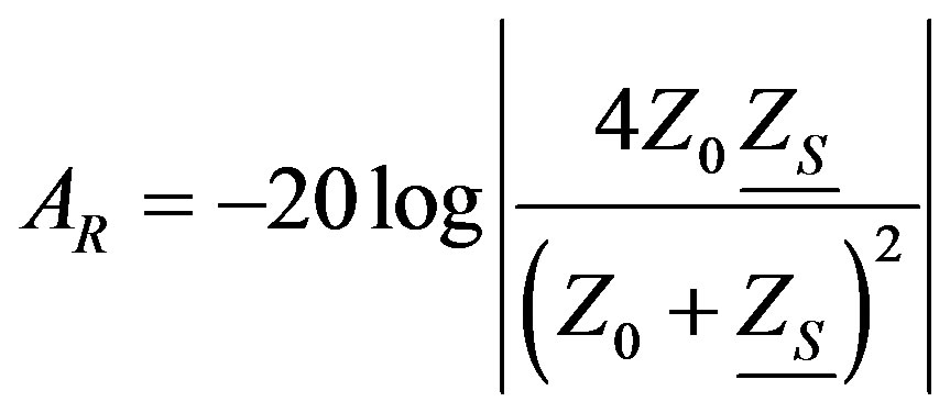
wave) to describe the attenuation brought by a shielding. Different causes of attenuation are enlightened: reflection (3), and multiple reflections (5), transmission (4) and the nature of the source in near field (6).
The reflection losses are due to the discontinuity of the characteristic impedance of the propagation medium. The reflection losses are given by (3). At the interface air/ shielding, a part of the energy of the incident wave is reflected and the other part propagates through the shielding. The transmitted wave is submitted to an attenuation inside the shielding (transmission losses (4)) which depends on the skin depth δ. Finally, the wave arrives on the shielding/air interface where a new reflection occurs.
 (3)
(3)
where Z0 is the characteristic impedance of free space (Z0 = µ0c0),  is the characteristic impedance inside the shielding.
 (4)
(4)
where t is the thickness of the shielding.
If the attenuation by transmission is low, multiple reflections inside the shielding can occur. In this case, a corrective term has to be added to AR and AA:AMR given by (5).
 (5)
(5)
In our application domain, magnetic sources in near field are considered. In this case, AR must be replaced by (6):
 (6)
(6)
where  is the characteristic impedance of magnetic near field, r is the distance between the magnetic source and the shielding. Finally, the total attenuation is the sum of (4)-(6). Figure 2 shows an example for a 2 mm copper shielding, 10 mm from the source. Each phenomenon is represented by its attenuation and is plotted versus the frequency. The total attenuation is also plotted on Figure 2.
4. 2D Numerical Approach
To consolidate the analytical approach, a 2D axisymetric modelling was implemented in a commercial electromagnetic software (Flux) developed by CEDRAT. This software uses the Finite Element Method (FEM) with a magneto dynamic formulation. Specific boundary conditions were used (infinite box) on the external boundaries of the problem because the magnetic field is not conducted by a magnetic material like in a transformer. Also, the coils are modelled as copper conductors and the mesh is adapted to take into account the skin depth (referred to the maximal frequency of interest). This restriction will impact on the maximal frequency of the numerical results (2 MHz in the air and 100 kHz with a shielding).
A first simulation was run with two coils in air. One is supplied with 1 A noted I1 (modulus) and the current in the second coil (in short circuit) noted I2 (modulus) is then computed. The attenuation in air is computed by (7)
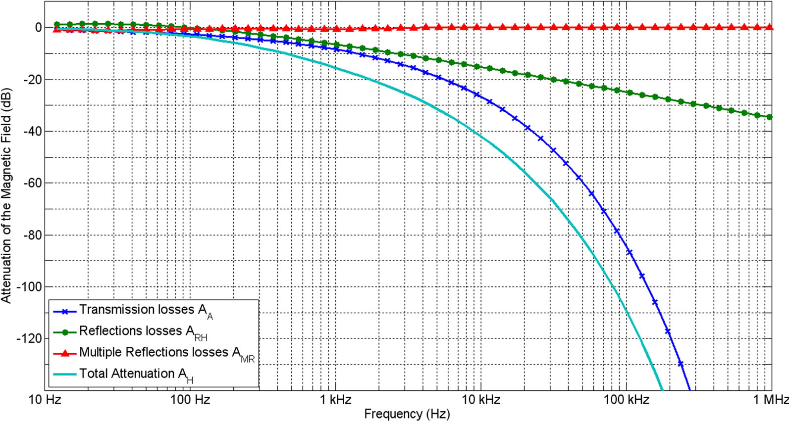
Figure 2. Different kinds of attenuations versus frequency for a 2 mm copper shielding 10 mm from the source.
for each frequency:
 (7)
(7)
Figure 3 shows analytical results [10], numerical 2D axisymetric results and experimental results. The two coils have 15 mm radius, one turn, the diameter of the wire is 0.6 mm and the distance between the two coils is 22 mm. Figure 4 shows a numerical result.
Then the same problem was computed with a shielding inserted between the two coils. Special attention is paid to the mesh inside the shielding: it must be adapted to the skin depth i.e. two layers of triangular elements by δ (referred to the maximal frequency). The attenuation noted A, given by (8), is obtained by subtracting the attenuation without shielding Aair (7) to the attenuation with shielding Ashield Ashield is computed according to (8) considering I2shield (the current in the short circuited coil with the shielding) when I1 is kept constant.
 (8)
(8)
 (9)
(9)
Figure 5 shows results for a 50 µm aluminum shielding. The numerical approach was used to study the influence of different parameters: the width of the sample of shielding compared to the diameter of the coils, the influence of the distance between the source and the shielding, the number of turns of the coils, to verify the validity of the proposed shielding specifications (example of Figure 1)… These results are essential to realize the sizing of the test bench.
Figure 9 shows for different frequencies the leakage coupling between the two coils versus the ratio noted Rleakage: width of the perfect shielding divided by the diameter of the coils. Results of Figure 4 show that a minimal value of Rleakage = 4 must be respected. Other unwanted couplings between the two coils can exist (capacitive coupling in common mode for example) and are not take into account in the FE modeling (magnetodynamic formulation). In the next section, the modifications made on the test bench to avoid this phenomenon will be explained.
5. Experimental Characterization
All the developed approaches previously presented (analytical and 2D numerical) are not enough versatile to help engineers to size a shielding for a given application with specific constrains. Indeed, new composite materials or multilayer shielding associating conductors, magnetic and dielectric layers cannot be used because of the lack of information concerning their global shielding properties. So, an experimental test bench is required to extract global properties of different kinds of materials.
5.1. Experimental Test Bench
The main constrains for the developed test bench are:
• Frequency range: 20 kHz - 30 MHz.
• Size of samples under test: 200 × 200 mm.
• Magnetic source (low level to begin).
• Distance source/shielding: few cm.
• Large dynamic range: 80 dB (see Figure 1).
• All the mechanical part of the bench should be transparent for the EM waves in the frequency range of interest.
Figure 6 shows a representation of the test bench.

Figure 3. Coupling of two coils in the air versus frequency.

Figure 4. Repartition of the H field between the two coils in air (f = 2 MHz). 2D axisymetric modeling. The lower antenna is supply with 1 A.
5.2. Sizing of Antenna
In this study, magnetic sources are considered. Loop antennas are thus chosen. To improve the coupling between the two coils (to maximize the dynamic range), the number of turns of each winding can be increased. However, the more the number of turns is, the more the capacitive coupling between turns is important and the more the frequency bandwidth of the antennas is limited.
Indeed, the upper limit of the bandwidth is fixed by the resonant frequency between the inductance of the antenna and the equivalent stray capacitance. Beyond this limit, the impedance of the antenna has a capacitive behavior which results in a minimization of the currents through all the turns and thus to the decrease of the field.
The other way to increase the coupling between coils is to reduce the distance between them. A distance of 27 mm was chosen between both antennas due to mechaniccal aspects (current probes…).
An analytical model was developed to size loop antennas of the test bench. It is based on [11] (10) for the inductive part, on [12] (11) for the capacitive coupling between turns and on [13] for the resistance depending on the frequency (skin effect) for the resistive part (12).
 (10)
(10)
where L is the inductance of the solenoid (H), N is the number of turns, D is the diameter of the solenoid (m), l is the length of the solenoid (m), k is the Nagaoka coefficient, depending on the solenoid geometry.

with
 (11)
(11)
where r is the radius of the coil wire without the insulator (m), N is the number of turns, t is the thickness of the insulating coating of the wire (m), εr is the relative permittivity of the insulator.
 (12)
(12)
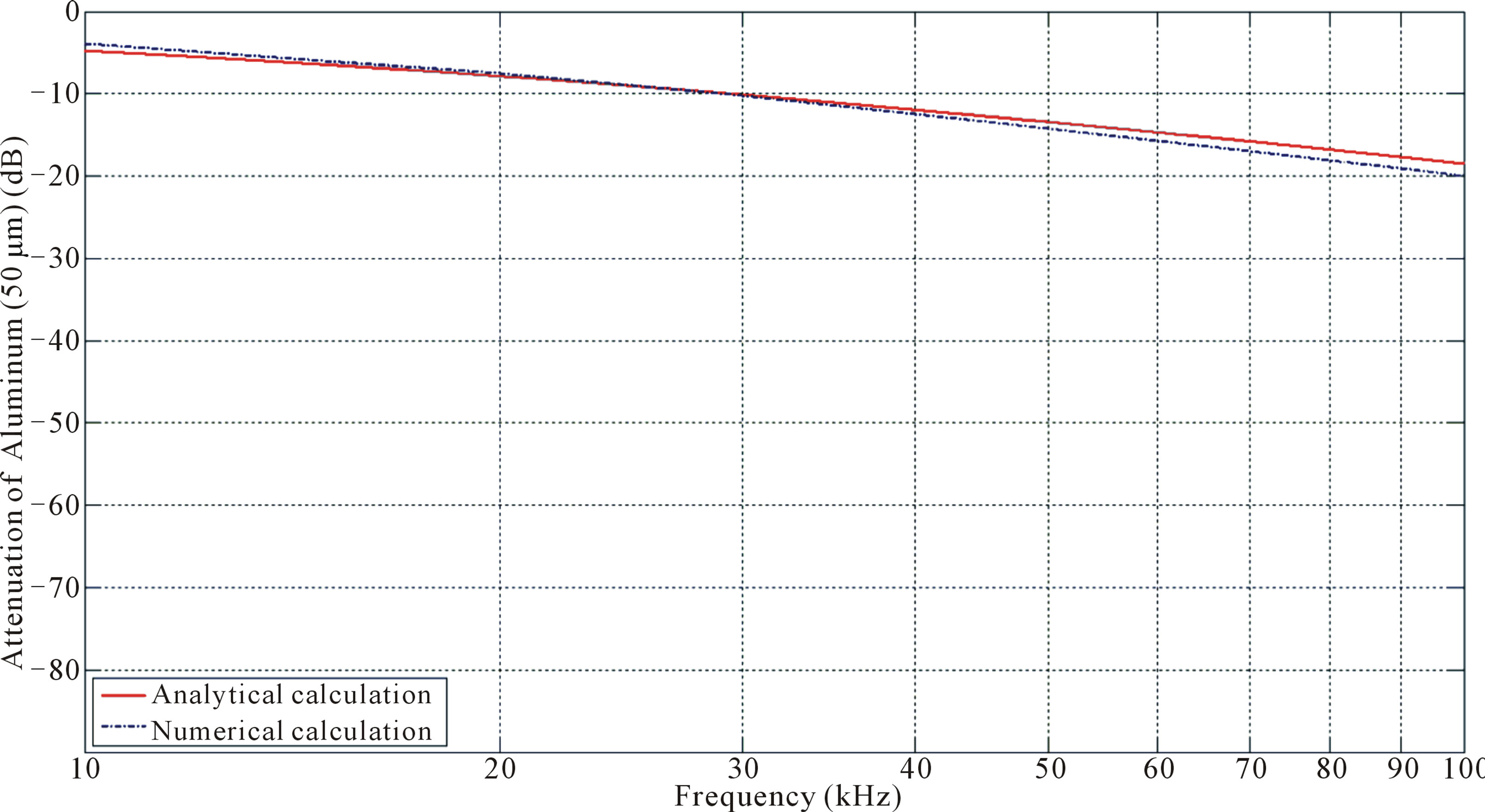
Figure 5. Attenuations for a 50 μm aluminum shielding versus frequency.
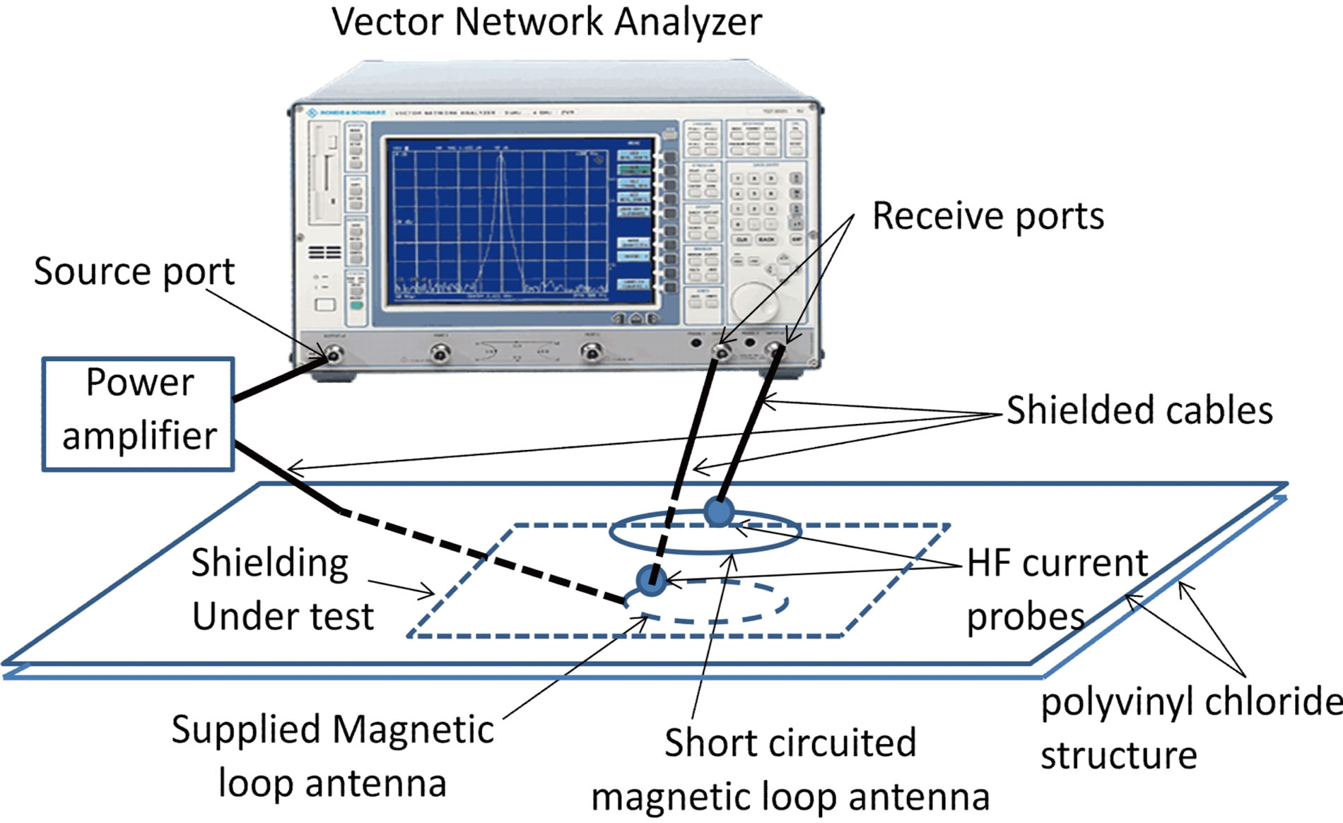
Figure 6. Representation of the test bench.
where σ is the electrical conductivity of the coil wire (S×m–1), r is the radius of the wire (m), δ is the depth skin (m), J0 and J1 are Bessel functions of the first kind.
Figure 7 show analytical and experimental impedance of antenna for different geometries of coils. Below the resonant frequency, impedances show an inductive behavior. As expected, the more the number of turns is important, the more the value of the equivalent inductance is high which represent to a more important generation of H field and therefore a better coupling with the second coil. The same phenomenon is observed concerning the diameter of the coils. The minimization of the number of turn allows to shift the resonant frequency and therefore to increase the frequency bandwidth of the antenna. In the case of a single-turn coil, the analytical expression given by (11) does not allow to calculate the capacitive term (its tends to infinity). Indeed, this one represents the potential difference between turns which is no more relevant in a single-turn configuration. So, to estimate the capacity, the contribution of the connectors and cables is no more negligible and it has to be considered in the expression of the total impedance. Unfortunately, it is very difficult to quantify it and that’s why there is only an experimental result on the fourth Figure 7(d). To evaluate the parasitic coupling between the two coils with a perfect shielding (disk of radius equal to 100 mm) a 2D FE approach was used. The disk is modelized as a Perfect Electric Conductor (PEC), so this shielding can be considered as perfect. The parasitic couplings are due to the field passing on the sides of the shielding. Figure 8" target="_self"> Figure 8 presents an example of repartition of magnetic field with a shielding modelized as a PEC. Figure 9 shows the amplitude of the parasitic coupling for different radius of the antennas versus the frequency.
The final sizing is a compromise between many elements: maximization of the magnetic coupling between antennas, use of antennas below their resonant frequency, minimization of the parasitic couplings between antennas (especially in high frequency).
Two loop antennas with a radius of 15 mm with 1 turn
 (a)
(a)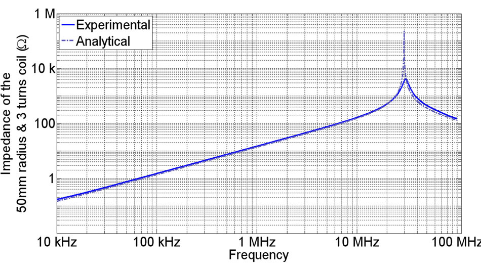 (b)
(b)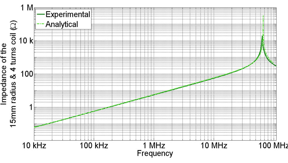 (c)
(c) (d)
(d)
Figure 7. Analytical and experimental results for different coils (a)-(d). (a) 50 mm radius and 4 turns coil; (b) 50 mm radius and 3 turns coil; (c) 15 mm radius and 4 turns coil; (d) 15 mm radius and 1 turn coil.
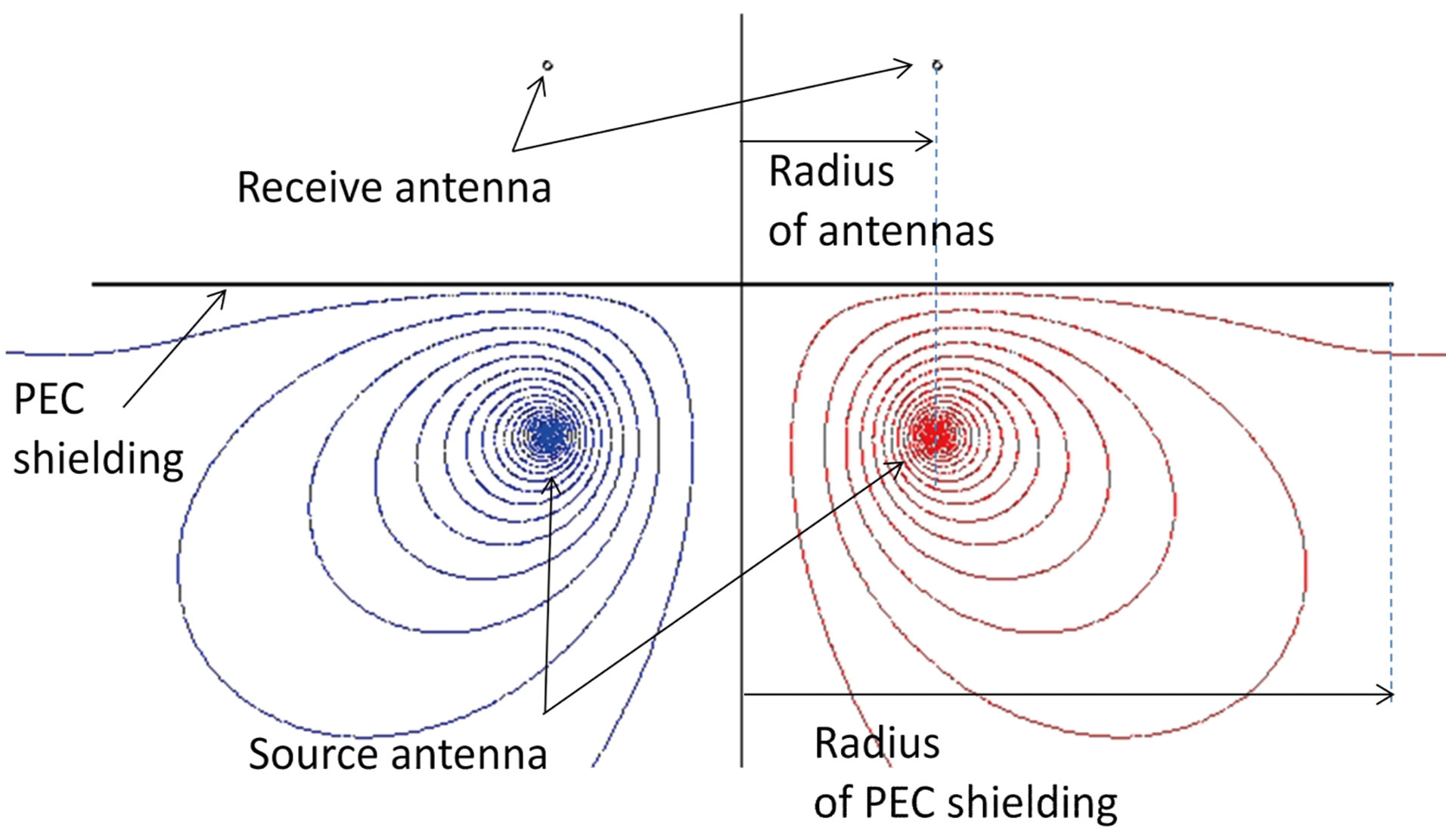
Figure 8. H field repartition for two loop antennas with a PEC shielding. The lower antenna is supplied with 1 A.
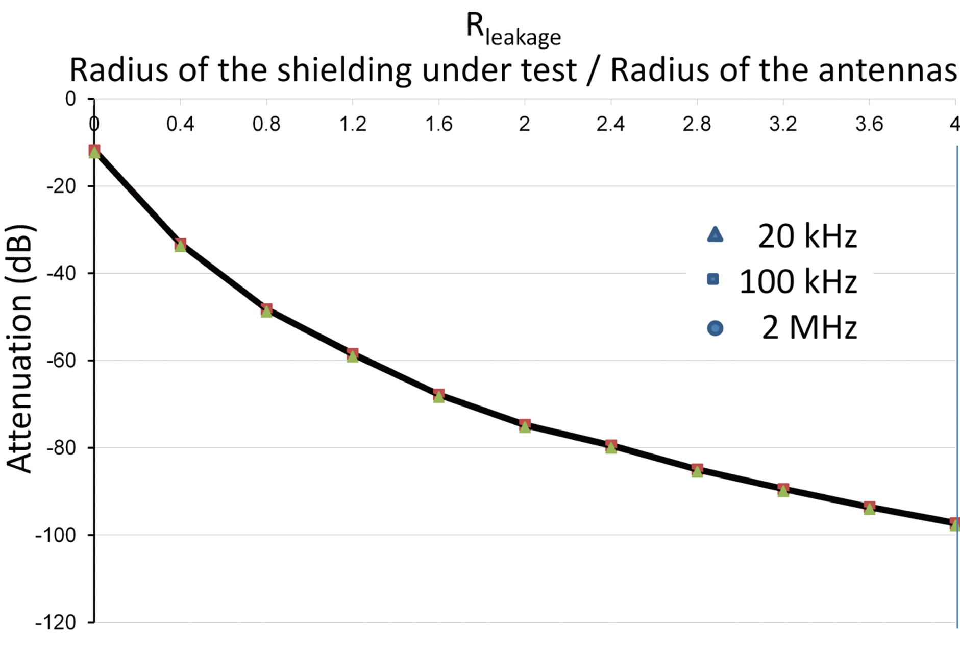
Figure 9. Magnetic parasitic coupling (dB) versus Rleakage for different frequencies.
and 4 turns short circuited were chosen for the source antenna and the receiving antenna respectively. Figure 11 shows the coupling between both coils without shielding and with a perfect shielding versus the frequency for different couples of antennas.
5.3. Description of the Test Bench
Figures 6 and 10 show the developed test bench. The mechanical structure is built in polyvinyl chloride. The source antenna (lower antenna) is supplied by the source port of the Vector Network Analyser (VNA) via a power amplifier and currents into the two coils are measured with two current probes (100 MHz of bandwidth) connected to the receive ports of the VNA (frequency domain measurement protocol). The first one, on the source, is a passive probe (Tektronix P6022). The second probe, on the receiver, is an active one (Tektronix TCPA300). The shielding under test is inserted between the two plates of polyvinyl chloride.
5.4. Experimental Protocol of Measurement
To extract the shielding efficiency, two methods are investigated in this study. The first one is a frequency do-
 (a)
(a) (b)
(b) (c)
(c)
Figure 10. Photos of the developed test bench, (a) Top view; (b) Upper antenna; (c) Bottom antenna. (a) Top view of the experimental bench; (b) Details of the upper antenna with the HF current probe; (c) Details of the lower antenna with its supply and the HF current probe.
main protocol using a VNA (Rohde & Schwarz ZVC). Three ports of the VNA in tracking mode are used. The a1 port (source port) generates a signal (1 V) which supplies a power amplifier (M2S A0122-50 Watts) connected to the lower coil of the testing bench. The b1 and b2 ports (receive ports) are connected to the two current probes, the current in the source antenna and the current in the receiving antenna respectively. The VNA calculates the ratio b2/b1 in tracking mode with the a1 port. The shielding attenuation noted A is obtained with (7), (13) and (14).
 (13)
(13)
I1shield is the current in the source antenna when the shield is inserted between the two coils. The current in the source antenna cannot be maintained constant in the measurement protocol because the a1 port is a voltage source and the current depends on the impedance of the coil. However, the ratio b2/b1 allows to compensate this dependence to the variation of impedance.
 (14)
(14)
Figure 11 presents an example of measurement. The noise floor (curve a) is obtained by inserting a very thick copper shielding (3 mm, equal to 6.5 δ in copper at 20 kHz). In this way we can consider that all coupling between both coils are parasitic. The red curve in the Figure 11 shows the attenuation (Aair) between both coils without shielding. We can observe the potential dynamic range which can be exploited during measurements (about 90 dB in the frequency band 100 kHz - 10 MHz).
To obtain a large dynamic range, the parasitic coupling between the two coils must be minimized. Several changes were realized to achieve this last point (Figure 10): ferrite cores are added on all the coaxial cables to limit common mode perturbations (parasitic capacitive couplings between shielding and coils), all the coaxial cables are fitted with a double shielding to avoid coupling with the active part of the cable. The shielding is grounded with one of the coaxial cable to charge-dissipating to ground and to short cut parasitic capacitors existing between coils and shielding.
The second method consists in a time domain measurement in which the signal is “extracted” from the noise thanks to a signal processing method. The same test bench is used where the source antenna is supplied by a sine generator but, contrary to the frequency method, measurements on the receiving antenna are made in the time domain using, for example, an oscilloscope. Then, a post-treatment using the relations (15) and (16) allows computing the Power Spectral Density (PSD) of the concerned signal from which it is possible to obtain its magnitude, and then the attenuation. Indeed, according to the signal processing theory, the PSD of a white noise is a constant whereas the PSD of a sine wave is a Dirac peak at the frequency of the signal. Consequently, given that the power of the signal is represented by Dirac while that of the white noise is constant over the frequency range, the magnitude of a sinusoidal wave is increased tenfold compared to the magnitude of a white noise.
The PSD is the Fourier transform of the autocorrelation of the signal. Below, the relation (15) shows the formula of the autocorrelation Rx(τ) of a signal x(t) and the relation (16), the PSD formula.
 (15)
(15)
 (16)
(16)
Theoretically, as the relation (17) shows, the PSD of a sine wave is two Dirac peaks at minus and plus the frequency of the initial signal. Moreover, the magnitude of the PSD is equal to a quarter of the square of the magnitude of the signal.
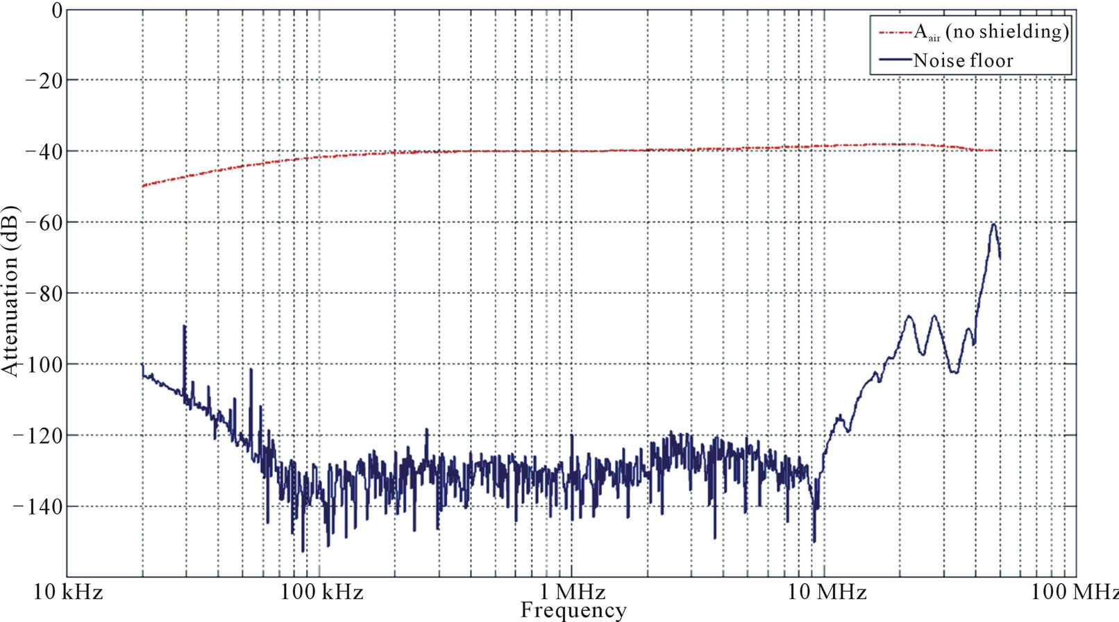
Figure 11. Attenuation between both coils with a thick shielding (noise floor) and without (Aair).
 (17)
(17)
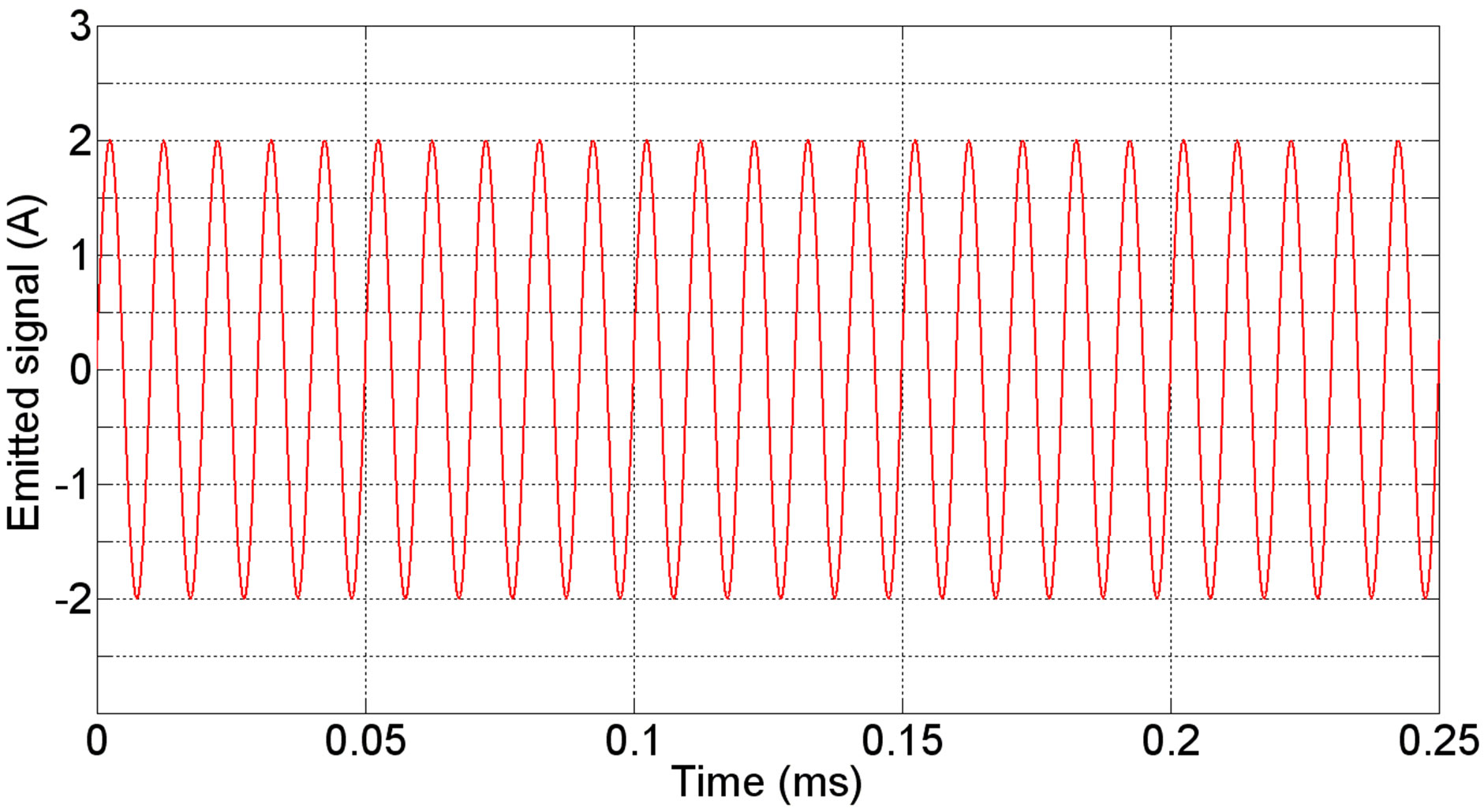
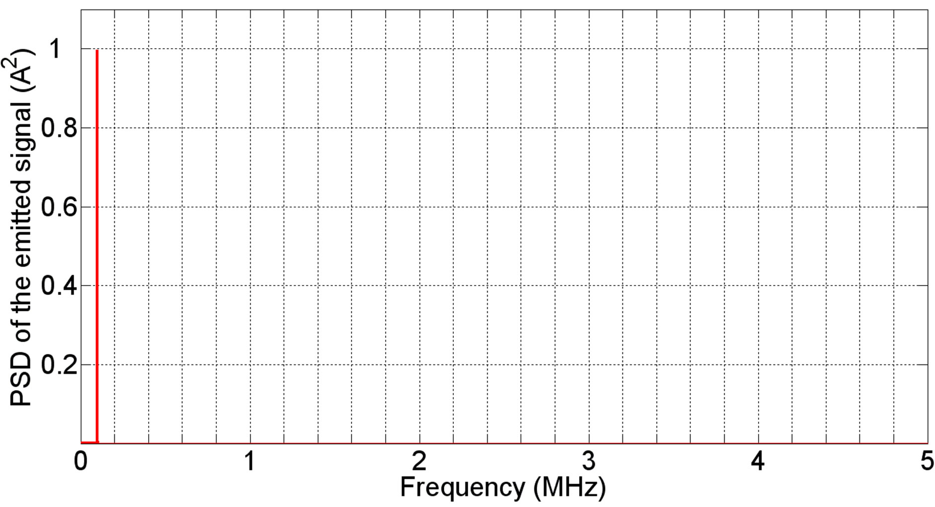
In order to validate the approach, an experiment was performed on the test bench where the two antennas were spaced 27 mm. The distance between the source and the shielding was 11 mm and the source antenna was supplied by a sine generator with a magnitude of 2 A and a frequency of 100 kHz. The shielding inserted was a 20 µm thick aluminum sheet. First, the time domain signals in the emitting and the receiving antenna are represented on Figure 12 and the PSD of both on Figure 13.
In this case, the Signal-to-Noise Ratio (SNR) is higher than usual in order to highlight the PSD effect. On the curve 13(b)), the magnitude of the PSD is equal to the sum of the magnitude of the PSD of the received signal and the PSD of the noise. So, the magnitude of the PSD of the cleared received signal is obtained by the difference between the total one and the one of the noise. In the example of the Figures 13 and 14, the mean value of the PSD of the noise is about 0.12 µA2. So, the magnitude of the PSD of the cleared received signal is about 3.95 µA2 which corresponds to a magnitude of the received signal of 4 mA. Thus, we can conclude that the emitted-to-received signals ratio is 500, equivalent to a 54 dB attenuation, which is expected. Indeed, as you can
 (a)
(a)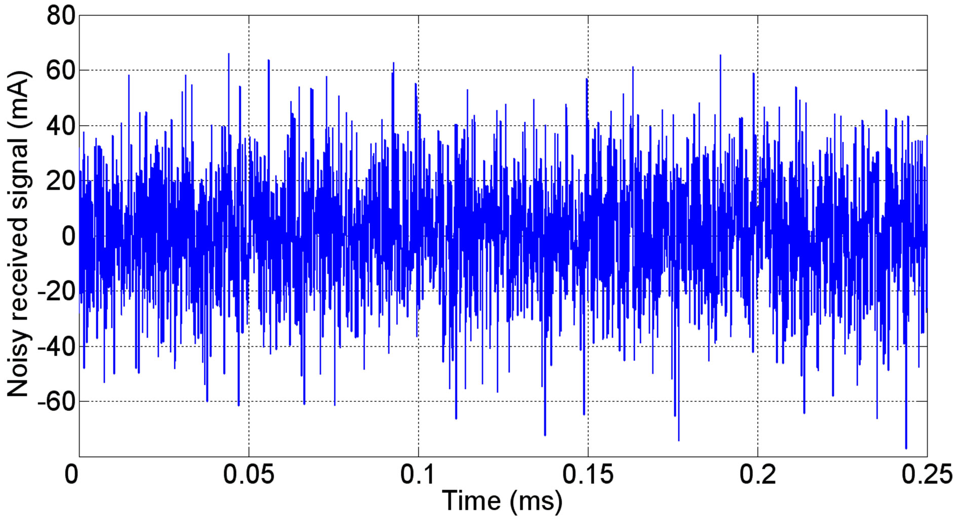 (b)
(b)
Figure 12. Time domain signals in the emitting (a) and receiving (b) antennas. (a) Emitted signal at 100 kHz (A).
 (a)
(a) (b)
(b)
Figure 13. PSD of the source (a) and the receiver (b) signals for positive frequencies. (a) PSD of the source (A2); (b) PSD of the receiver (μA2).
see on Figure 14, the attenuation of a 20 µm thick aluminum sheet is about 11 dB around 100 kHz. Moreover, the non-perfect coupling between antennas induced losses of about 42 dB at 100 kHz (Figure 11). Eventually, the total attenuation (shielding plus air) is 53 dB which the time-domain result satisfying. The frequency domain method is easiest to operate because it is completely automatic in tracking mode. The time domain method can be interesting in low frequency (under 20 kHz because the VNA cannot operate under this frequency) or for some frequencies where the dynamic range of the VNA is not sufficient.
6. Validation
Figure 14 shows analytical, 2D FE and experimental results for a 20 µm aluminum shielding. We can observe a good adequacy between experimental and theoretical results for a frequency range starting from 20 kHz (minimal functioning frequency of the VNA) up to 25 MHz (at this frequency, the attenuation meets the noise floor).
As we have seen, analytical and numerical models fit properly the experimental results obtained on the test bench. Thus, it seems logical to explore the possibilities, in terms of shielding efficiency, of different materials.
Nevertheless, these models need the precise knowledge of the electromagnetic characteristics of materials (σ, μ, ε) to be run and to give correct results. These parameters can easily be obtained in the case of simple materials (homogeneous ones) but, conversely, it is very complicated to get them when the considered medium is complex. For example, a material made with several homogeneous parts is complex and it will be very difficult to determinate its shielding efficiency thanks to analytical or numerical model. Likewise, non conductive mediums including conductive fibers are very complex because the exact organization of the fibers is unknown.
Anyway, the role of the test bench is precisely to test complex materials in order to get the shielding attenuation where theoretical models cannot. Figure 15 shows the example of a polyester compound containing 40% of carbon fibers. The medium is obviously non conductive while the fibers are.
7. Conclusion
Because of news applications of power electronics systems in many domains like transport: more electric aircrafts or electric cars, EMC has to be integrated early in the design flow of the complete system (aircraft or car).
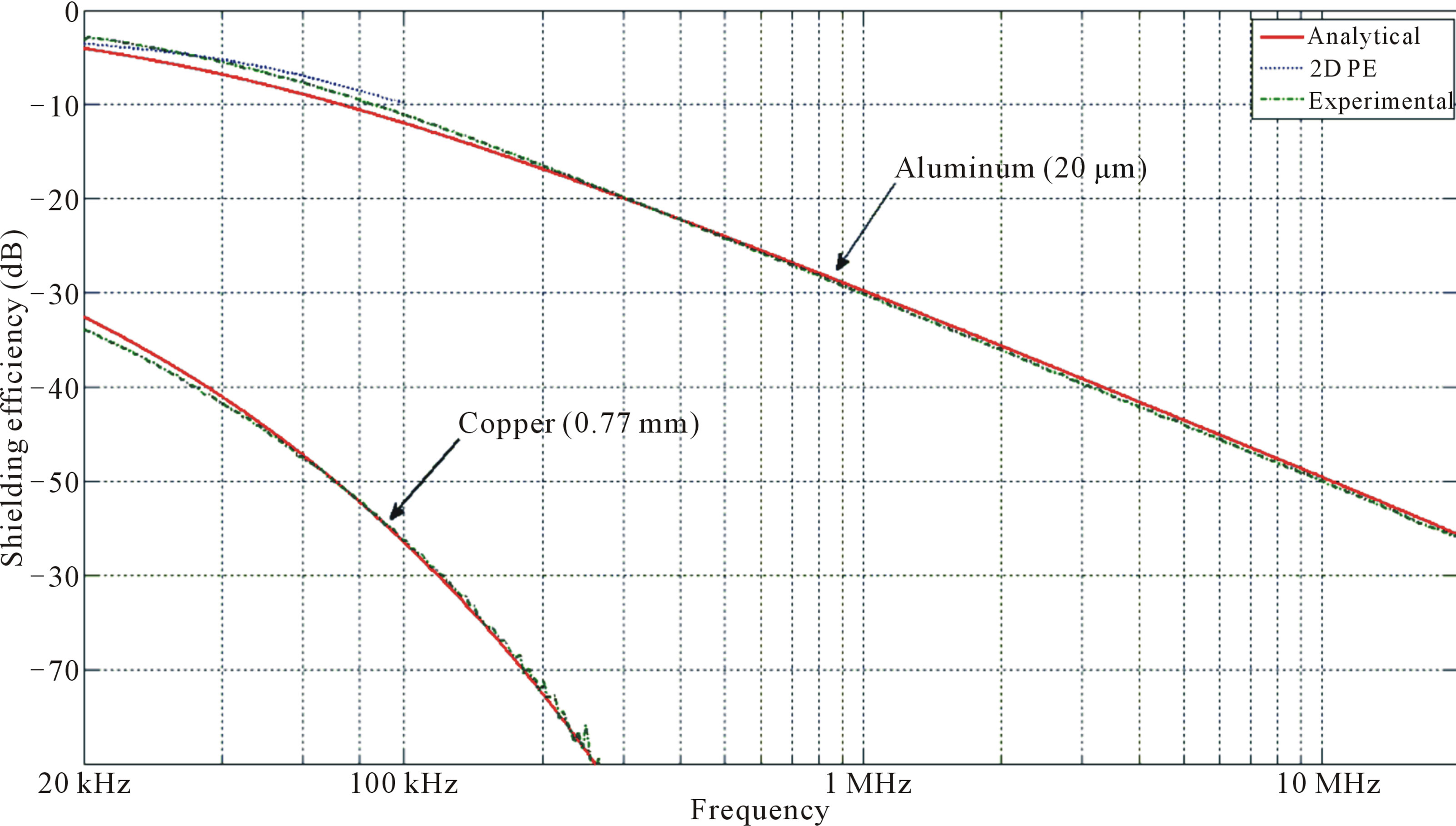
Figure 14. Attenuations of a 20 μm aluminum shielding (analytical, 2D FE and experimental results) and a 0.75 mm copper shielding (analytical and experimental results).
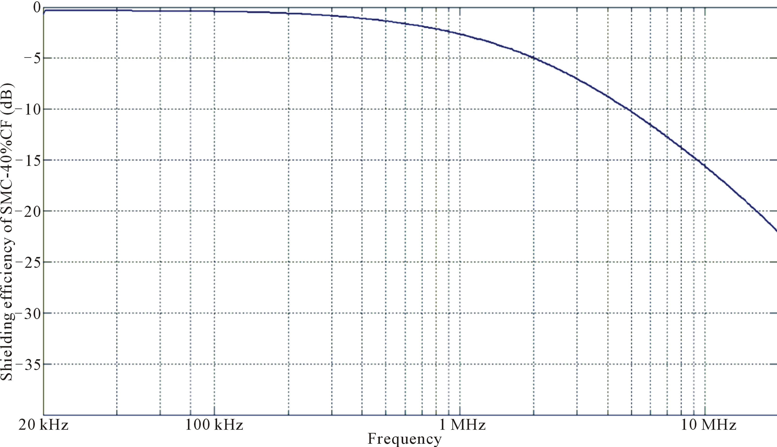
Figure 15. Attenuation of a 3 mm shielding of SMC with 40% of carbon fibers.
The shielding is one of the most used solutions to avoid unwanted couplings between power systems and their environment. We have presented a new experimental solution to determine the shielding efficiency of different material (metallic or composite materials) in the frequency domain of power electronic applications (some kHz to few MHz).
REFERENCES
- IEEE, “C95.1, IEEE Standard for Safety Levels with Respect to Human Exposure to Radio Frequency Electromagnetic Fields, 3 kHz to 300 GHz,” International Committee on Electromagnetic Safety (ICES), 2005.
- BALANIS C.A., “Advanced Engineering Electromagnetics,” Wiley, Hoboken, 1989, p. 1008.
- NF EN 50147-1, “Anechoic Chambers—Part 1: Shield Attenuation Measurement,” 1997, p. 11.
- NF EN 61000-4-23, “Electromagnetic Compatibility (EMC)—Part 4-23: Testing and Measurement Techniques—Test Methods for Protective Devices for HEMP and Other Radiated Disturbances,” 2001, p. 93.
- NF EN 61000-5-7, “Electromagnetic Compatibility (EMC)—Part 5-7: Installation and Mitigation Guidelines—Degrees of Protection by Enclosures against Electromagnetic Disturbances (EM Code),” 2001, p. 29.
- NF EN 61587-3, “Mechanical Structures for Electronic Equipment—Tests for IEC 60917 and IEC 60297—Part 3: Electromagnetic Shielding Performance Tests for Cabinets, Racks and Subracks,” 2007, p. 17.
- W. Potocki, “Avro Arrow: The Story of the Avro Arrow from Its Evolution to Its Extinction,” Boston Mills Press, Erin, 2004, pp. 83-85.
- S. Anwar and B. Zheng, “An Antilock-Braking Algorithm for an Eddy-Current-Based Brake-by-Wire System,” IEEE Transactions on Vehicular Technology, Vol. 56, No. 3, 2007, pp. 1100-1107. doi:10.1109/TVT.2007.895604
- ISO 11452-2.
- E. Durand, “Électrostatique et Magnétostatique,” Masson, Paris, 1953, p. 774.
- H. Nagaoka, “The Inductance Coefficients of Solenoids,” Journal of the College of Science, Imperial University, Tokyo, Vol. 27, Article 6, 1909, p. 33.
- G. Grandi, M. K. Kazimierczuk, A. Massarini and U. Reggiani, “Stray Capacitances of Single-Layer Solenoid Air-Core Inductors,” IEEE Transactions on Industry Applications, Vol. 35, No. 5, 1999, pp. 1162-1168. doi:10.1109/28.793378
- G. Fournet, “Électromagnétisme,” Techniques de l’Ingénieur, 1993, p. 90.