Journal of Electromagnetic Analysis and Applications
Vol. 2 No. 3 (2010) , Article ID: 1541 , 17 pages DOI:10.4236/jemaa.2010.23022
Modeling of Multi-Pulse VSC Based SSSC and STATCOM
![]()
1Graduate Program in Electrical Engineering, CUCEI University of Guadalajara, Guadalajara, Mexico; 2Power Systems Department, CINVESTAV, Guadalajara, Mexico.
Email: pavel.zuniga@cucei.udg.mx, jramirez@gdl.cinvestav.mx
Received October 27th, 2009; revised November 16th, 2009; accepted November 19th, 2009.
Keywords: Commutations, Harmonics, Multi-Pulse, Modeling, SSSC, STATCOM
ABSTRACT
The aim of this paper is to contribute to the dynamic modeling of multi-pulse voltage sourced converter based static synchronous series compensator and static synchronous compensator. Details about the internal functioning and topology connections are given in order to understand the multi-pulse converter. Using the 24 and 48-pulse topologies switching functions models are presented. The models correctly represent commutations of semiconductor devices in multi-pulse converters, which consequently allows a precise representation of harmonic components. Additionally, time domain models that represent harmonic components are derived based on the switching functions models. Switching functions, as well as time domain models are carried out in the original abc power system coordinates. Effectiveness and precision of the models are validated against simulations performed in Matlab/Simulink®. Additionally, in order to accomplish a more realistic comparison, a laboratory prototype set up is used to assess simulated waveforms.
1. Introduction
Most of the existing converter based Flexible AC Transmission Systems (FACTS) devices rated above 80MVAR use either 24 or 48-pulse converters [1–5], because they exhibit several advantages over other Voltage Sourced Converter (VSC) configurations. Some of the key advantages include harmonic content, switching frequency and dc capacitor rating.
The harmonic content of the output voltage generated by a multi-pulse converter is low; the converter harmonic components are in the order of n = 6km ± 1, where m = 0, 1, 2,…, and k is the number of 6-pulse units used to construct the VSC. The harmonic amplitudes of these components are 2k/nπ times the dc side voltage magnitude used by the converter. This reduces the harmonics injected by the VSC to the power system. In comparison to other VSC topologies the multi-pulse converter has a superior total harmonic distortion for a given number of semiconductor switches [6].
The switching frequency of the commutating devices for a power converter is severely limited and must be kept low. The multi-pulse converter has the same switching frequency as the fundamental frequency of the output voltage, which is also very low, 60 Hz switching frequency for a 60 Hz utility voltage. This limits the switching losses as well as the heat in the commutating devices.
The rated voltage of the dc capacitor is low, which reduces physical volume of the multi-pulse VSC in favor of economical considerations. The capacitor voltage ripple decreases as the number of pulses of a given configuration increase; therefore, in high pulse configurations the dc capacitor rating can be reduced without compromising the ripple level of the dc voltage.
Frequently, the multi-pulse VSC dynamic models used are the dq0 [5–12], and the Fundamental Frequency (FF) models in abc coordinates [5–9]. dq0 models are widely used due to simplification of model computations specially when working with the synchronous generator, because they convert balanced three phase sinusoidal signals into constants. The set of abc quantities are transformed into a synchronously rotating reference frame using the so called dq0 or Park’s transformation; as a result, the inverse transformation is needed if the phase quantities have to be obtained from dq0 signals. On the other hand three phase models are derived directly from the system; therefore, the obtained signals are in their original abc coordinates. FF models represent VSC’s with fundamental frequency components only and do not take into account harmonics in their signals. To overcome the lack of proper harmonic representation in simplified models, Switching Functions (SF) modeling in abc coordinates is accomplished, so as to obtain realistic characterization of VSC devices performance inserted in a power system. Moreover, reduced Time Domain (TD) models that also consider harmonic components are obtained using the derived SF models. In addition, since the SF and TD models include ac and dc side converter harmonics, control strategies as well as the power system, other controllers, system protections, etc. would be subjected to a more realistic interpretation of a VSC device than when using simplified models.
2. Multi-Pulse VSC Topology
The objective of a VSC is to generate three phase ac voltages using a dc voltage. The basic 6-pulse VSC configuration depicted in Figure 1 shows asymmetric turnoff devices with a parallel diode connected in reverse [13]. The frequency and phase of the three phase voltages generated by the 6-pulse VSC configuration are determined by the gate pulse pattern (GPP) of the commutating devices shown in Figure 2 [14]. The amplitude of the three phase ac voltages is determined by the magnitude of the dc voltage, vdc. The on-off sequence depicted in Figure 2 applied to the 6-pulse VSC shown in Figure 1 results in phase, va6, and line, vab6, voltages for phase a like the ones exhibited in Figure 3. The harmonic components of these signals are in the order of n = 6m ± 1, where m = 0,1,2, …, and the peak amplitude of the fundamental and harmonic components of va6 and vab6 are given by va6n = 2vdc/nπ and vab6n = 2 vdc/nπ, respectively.
Signals gs1, gs2, gs3, gs4, gs5 and gs6 are gate pulses of switches S1, S2, S3, S4, S5 and S6 in Figure 1, respectively. The gate signals can only take values of 0 or 1 for the switching devices to be off or on, respectively.
Inspecting Figure 3 it can be seen that even though these 6-pulse voltages are ac waveforms, they are not sinusoidal; this is due to a high harmonic content present in them.
In order to reduce the harmonic content of the resulting voltages, higher pulse configurations are needed, so as to cancel specific harmonic components. These arrangements are achieved combining 6-pulse VSC’s in order to produce an output voltage with reduced harmonics. The combination is made using transformer arrangements in a magnetic coupling circuit (MCC) and phase shifting transformer (PST). As a result, combining two 6-pulse VSC’s a 12-pulse configuration is attained, two 12-pulse converters achieve a 24-pulse topology and two 24-pulse arrangements result in a 48-pulse VSC. The 24 and 48-pulse converter configurations are depicted in Figure 4.
To combine the output voltages of the two 6-pulse VSC’s needed to achieve a 12-pulse configuration, a

Figure 1. Configuration of 6-pulse VSC
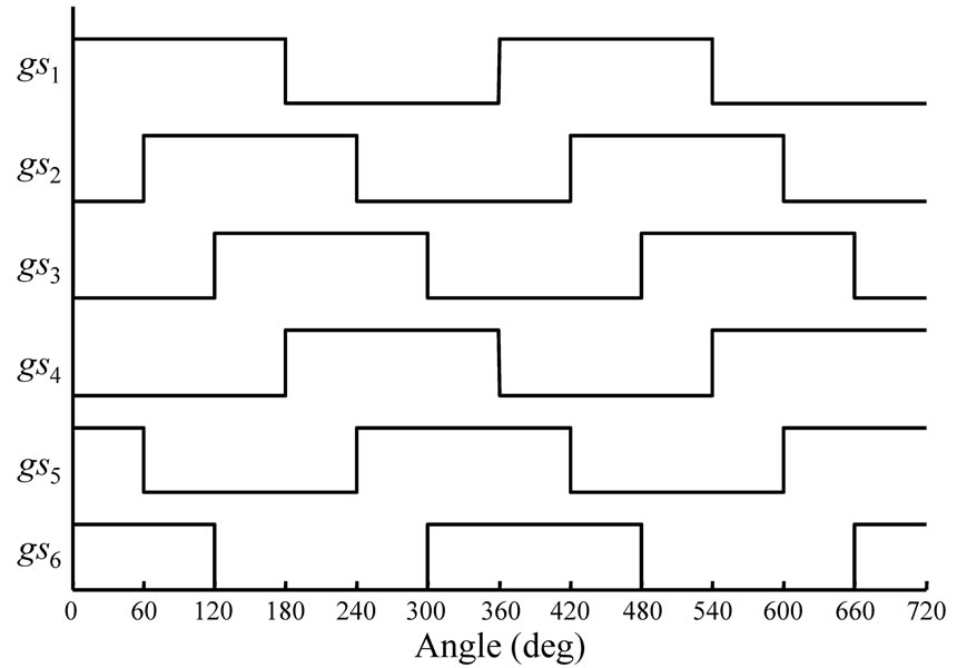
Figure 2. Gate pulse pattern of 6-pulse VSC

Figure 3. Phase and line voltages of 6-pulse VSC
MCC is needed in order to align and scale the harmonic components to be cancelled. The circuit consists of two transformers, a star-star (Y-Y) transformer with a turn ratio of  and a delta-star (Δ-Y) transformer with a turn ratio of
 . Also, the GPP of one VSC must lag 30° the phase angle of the other one. However, in order to obtain an appropriate output voltage, the combination of 6-pulse VSC’s to construct 24 or 48-pulse converters is achieved via a MCC and PST’s.
Due to the reduced harmonics of the 24 and 48-pulse VSC’s, these are configurations suitable for connection to the power system [1–3].
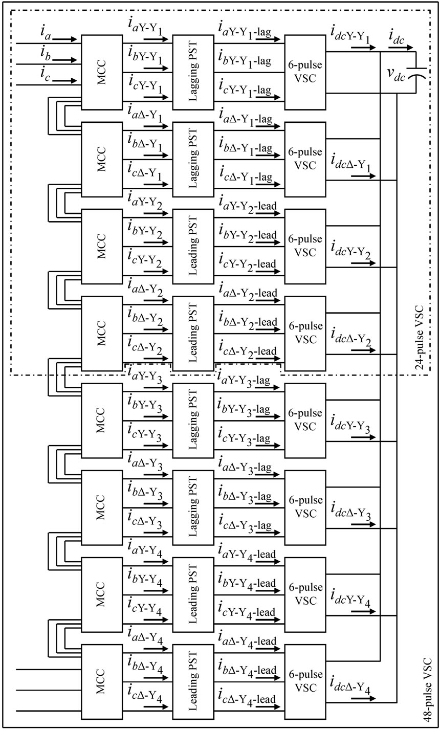
Figure 4. Topologies of 24 and 48-pulse VSC’s
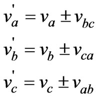
In order to create a 24 or 48-pulse waveform with a harmonic content of n = 24m ± 1 or n = 48m ± 1, respectively, where m = 0, 1, 2, …, the 6-pulse converters need relative phase displacements accomplished via the GPP that determines the angle of the resulting three phase output voltages. Also, PST’s are needed connected in series with the phase voltages in the primary side of the MCC transformers to add voltage components in quadrature. These quadrature voltages are obtained from the three phase output voltages of each VSC. The relations that produce the desired phase shifts are given by,
 (1)
(1)
where va’, vb’ and vc’ are the desired phase shifted voltages. The line voltages are added in order to generate a lagging phase voltage and subtracted to create a leading one.
Voltages vbc, vca and vab must have the specific amplitude to produce the desired phase shift angle; these amplitudes are determined by the transformation ratio of the PST’s, given by ξ = tan(φ)/ , where φ is the desired phase shift angle.
The analysis of the currents of the VSC topologies shown in Figure 4 is now addressed. The derivation of the expressions starts with the line currents, ia, ib and ic flowing into the VSC and finishes with the derivation of the dc current, idc.
Let us begin from the basic 6-pulse VSC shown in Figure 1. To derive the currents flowing into the VSC it is necessary to account for the configuration of the coupling transformer.
Neglecting losses, the currents flowing in the secondary side equals the currents in the primary side in a Y-Y configuration; therefore, the line currents match the VSC currents,
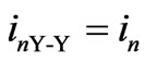 (2)
(2)
where n = a, b, c.
Once these currents are derived, the capacitor current, idc, is determined. The dc current is constructed adding segments of line currents [7]. The segments depend on which switch-diode, S-D, pair is conducting. Analyzing the upper S-D pairs of the 6-pulse VSC shown in Figure 1, it is observed that pairs S1-D1, S3-D3 and S5-D5 participate in idc, thus,
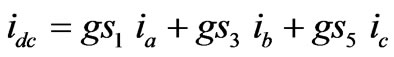 (3)
(3)
The above is a simple procedure useful for the analysis of higher pulse arrangements. Using this procedure and considering the configuration of the MCC, the 12-pulse current is obtained.
In the Δ-Y arrangement both the configuration and the turn ratio must be taken into account. Neglecting losses, the currents flowing out of the Δ-Y configuration are derived using the following relations,
 (4)
(4)
where iaΔ-Y, ibΔ-Y and icΔ-Y are the currents flowing out of the Δ-Y arrangement.
Since the currents flowing out of the MCC are the ones entering the 6-pulse units, these are used to obtain the two 6-pulse dc currents that shape the 12-pulse capacitor current.
Using (3) in each of the two 6-pulse units both components of the 12-pulse dc current are calculated, which together become the 12-pulse capacitor current, given by,
 (5)
(5)
where idcY-Y and idcΔ-Y are the 6-pulse dc currents flowing out of the Y-Y and Δ-Y transformers, respectively.
To derive the 24-pulse VSC currents, not only the MCC, but also the PST’s have to be included.
The 24-pulse VSC is constructed with two 12-pulse VSC’s, therefore the MCC operates using two Y-Y and two Δ-Y transformers. To calculate the currents of each Y-Y and Δ-Y transformer the same procedure as for the 12-pulse SSSC is carried out, therefore (2) and (4) are used. The effect of each PST has to be considered for the currents of the Y-Y and Δ-Y transformers as follows.
For the lagging configuration of the corresponding PST’s the relations are given by,
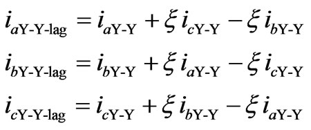 (6)
(6)
where ξ is the transformation ratio to achieve the desired phase shift angle; iaY-Y, ibY-Y and icY-Y are currents that come out of the Y-Y coupling transformers but can be interchanged for currents from the Δ-Y coupling transformers as needed; iaY-Y-lag, ibY-Y-lag and icY-Y-lag are currents that come out of the PST’s in the lagging configuration connected to the Y-Y coupling transformers.
For the leading configuration of the corresponding PST’s the relations are shown below,
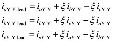 (7)
(7)
where iaY-Y-lead, ibY-Y-lead and icY-Y-lead are the currents that come out of the PST’s in the leading configuration connected to the Y-Y coupling transformers. The currents coming out of the PST’s in both cases are the VSC currents. Now the contribution of each VSC to idc can be derived and is given by,
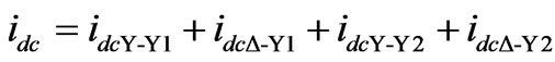 (8)
(8)
For the 48-pulse VSC, the configuration has to be taken into account as shown in Figure 4, however, the relations that apply to the 24-pulse converter also are valid for the 48-pulse topology. The contribution of each VSC to the capacitor current can be derived and is given by,
 (9)
(9)
The calculation of the VSC currents is made backwards, starting from the capacitor current equation and substituting the appropriate relations based on the line currents. The procedure is explained now step by step:
1) - Use the idc Equation, (8) for the 24-pulse VSC.
2) - Substitute in idc the corresponding current contribution of each 6-pulse unit, based in (3).
3) - For the 24-pulse VSC, the line currents are not used in (3), instead, the currents used are the ones flowing out of the PST’s depending on the configuration needed; the Equations used for these currents are (6) and (7) for the lagging and leading configurations, respectively.
4) - Finally, substitute the corresponding currents flowing into the PST’s in terms of the line currents as given by (2) and (4) for the Y-Y and Δ-Y configurations, respectively.
A similar procedure is used for the 48-pulse VSC currents, taking into account the appropriate relations.
Calculation of the voltages is achieved in a similar manner as derivation of the currents. Therefore, the MCC, PST’s and GPP have to be taken into account. For a thorough description of 24 and 48-pulse VSC’s refer to [15,16].
3. Multi-Pulse VSC Modeling
The multi-pulse VSC arrangements shown in Figure 4 are the building blocks of several FACTS devices, including the ones presented in this article.
The proposed mathematical models are derived using equivalent circuits for Static Synchronous Series Compensator (SSSC) and Static Synchronous Compensator (STATCOM). The connection of the devices to the power system depends on the type of compensation needed. The modeling of the devices is similar because their building block is the VSC; the difference is in their connection to the power system.
The main function of the SSSC is to provide series reactive compensation of transmission lines in order to regulate power flow; therefore, it is connected in series to a transmission line. The STATCOM major purpose is to provide shunt reactive compensation of voltage nodes in order to regulate voltage magnitudes; hence, it is shunt connected to a voltage node.
The control variable of the VSC, regardless of the connection to the power system and the multi-pulse configuration, is the phase angle applied to the gate pulse pattern of the commutating devices.
The modeling of SSSC and STATCOM take into account the number of 6-pulse VSC units in each multi-pulse configuration by considering the gate pulse pattern applied, as well as magnetic coupling circuit arrangement and phase shifting transformers.
3.1 Switching Functions Modeling
The SSSC model is derived using the system of Figure 5. The figure shows the SSSC equivalent circuit connected in series to a transmission line. The SSSC injected voltages are denoted by vase, vbse and vcse. Parameters Rse and Lse represent the common influence of both, series MCC and transmission line between sending and receiving end nodes denoted by subscripts s and r, respectively. The dc side of the SSSC is represented by a current source connected to a capacitor. Shunt connection of a resistance enables representation of converter losses.
From Figure 5 the equations that describe the currents of phases a, b and c are expressed as,
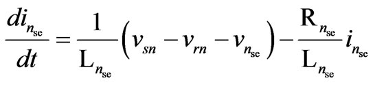 (10)
(10)
n=a, b, c For the dc circuit the expression that describes the behavior of the dc voltage is given by,
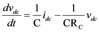 (11)
(11)
In order to derive the SF models, the configuration of the VSC, MCC and PST’s, as well as the GPP of the commutating devices have to be taken into account.
Let us begin from the basic 6-pulse VSC shown in Figure 1. To derive the 6-pulse SSSC SF model, the 6-pulse output voltages and the corresponding capacitor current need to be substituted in (10–11).
The SF model takes into account the 6-pulse converter gate signals shown in Figure 2.
Considering the GPP of Figure 2, the line and phase voltages of a 6-pulse VSC in terms of its gate signals yield,
 (12)
(12)
and
 (13)
(13)
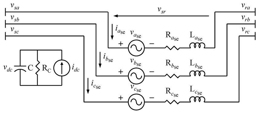
Figure 5. SSSC equivalent circuit connected in series to a transmission line
These are the switching functions voltages present in a VSC like the one shown in Figure 1.
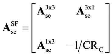
Substituting the 6-pulse voltages of (13) in (10) and the 6-pulse capacitor current of (3) in (11) and arranging in state space form, the 6-pulse SF model results,
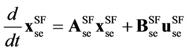 (14)
(14)
 ,
, 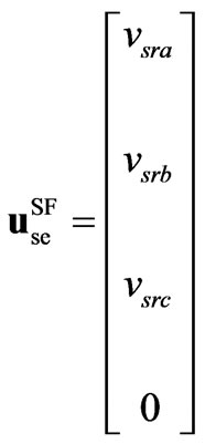
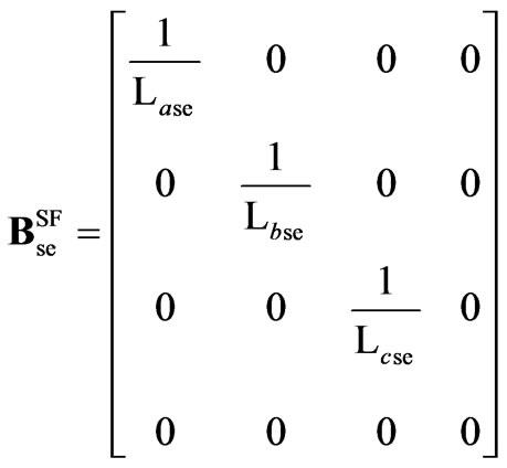
 ,
, 
 ,
, 
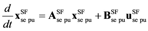
where superscript SF denotes switching functions model vectors and matrices.
Coefficients in  are given by,
 ,
, 
 ,
,  ,
, 
where superscript 6 denotes 6-pulse model coefficients.
As for the 6-pulse SF model, the elements needed to derive higher pulse SF models are the VSC output voltages and the corresponding capacitor current. The multi-pulse VSC configurations shown in Figure 4 are used to derive the corresponding VSC currents and voltages.
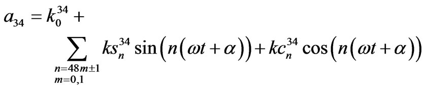
The resulting 12, 24 and 48-pulse SF models are similar to (14) except that coefficients in  are given in appendix A.
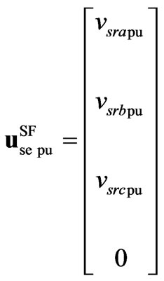
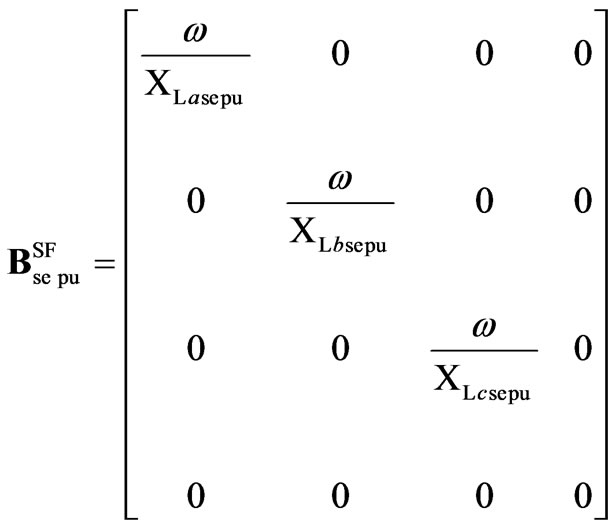
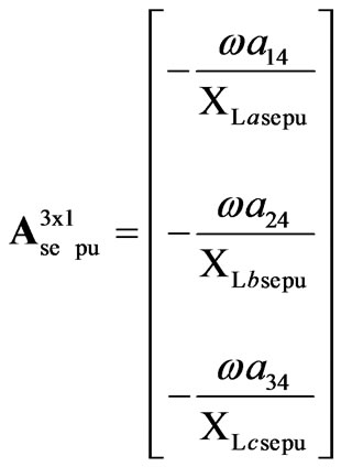
Additionally, the representation in (14) can be expressed in pu system as,
 (15)
(15)
 ,
, 


 ,
,  ,
, 
 ,
, 
where subscript pu denotes variables and parameters in per unit system.
The coefficients of the SF models in pu for 12, 24 and 48-pulse arrangements are given in appendix A.
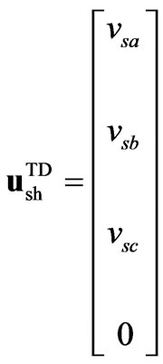
Now, the STATCOM modeling is addressed based on the similarities with the SSSC. The model is derived using the equivalent circuit of Figure 6. The figure shows the STATCOM connected to a voltage node. On the ac side the STATCOM is characterized by a three phase shunt connected sinusoidal voltage source that denotes its voltage injections for phases a, b and c expressed by vash, vbsh and vcsh, respectively. Parameters Rsh and Lsh represent the influence of the shunt coupling transformer connected to a voltage node denoted by subscript s. The dc side of the STATCOM is represented by a current source connected to a capacitor. Shunt connection of a resistance enables representation of converter losses.
By simple examination it can be seen that the SSSC and STATCOM schematic diagrams are very similar. If the receiving end node, vr, in Figure 5 is considered to be zero potential (ground), the resulting circuit is the one shown in Figure 6. Therefore, the equations that describe the STATCOM phase currents are similar to (10), except that the receiving end node voltages, vr, are zero. The dc

Figure 6. STATCOM equivalent circuit shunt connected to a voltage node
circuit expression that describes the behavior of the dc voltage is (11).
Considering the dc circuit equation (11) and the modified ac one (10), the SF modeling of STATCOM becomes,
 (16)
(16)
 ,
,  ,
,  ,
, 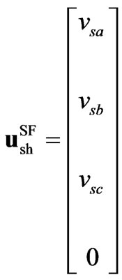
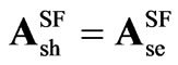
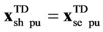
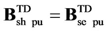
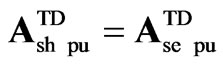
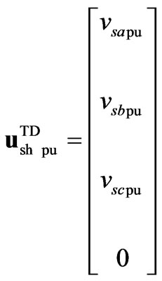
The model in (16) is very similar to the one in (14), except for vector ; also the variables and parameters for the SSSC models denoted by subscript se, are substituted for the STATCOM ones denoted by subscript sh.
The coefficients in  are the ones in
  for 6, 12, 24 and 48-pulse SF models, and are given in appendix A.
Similar to the SSSC modeling, (16) can be expressed in pu system as,
 (17)
(17)
 ,
,  ,
, 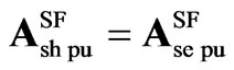

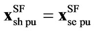
The representation in (17) is very similar to the one in (15), except for vector ; also the variables and parameters for the SSSC model denoted by subscript se, are substituted for the STATCOM model ones denoted by subscript sh. The pu variables and parameters are given in (15). The coefficients of the SF models in pu for 12, 24 and 48-pulse topologies are given in Appendix A.
3.2 Time Domain Modeling Considering Harmonics
The time domain models that consider harmonic components are obtained directly from the switching functions models, therefore, they are in three phase abc coordinates.
The TD models derived are intended to be reduced order models that enable simulation of multi-pulse SSSC and STATCOM devices, however, although they are reduced models, still represent harmonic components in waveforms of VSC devices.
The SSSC model is derived using the system shown in Figure 5. Therefore, the equations that describe the three phase currents and dc circuit voltage of the SSSC are given by (10) and (11).
The TD models are obtained using the state space SF representation given in (14). The derivation of the models is based on the representation of each converter switching functions by its Fourier series. Truncation of the Fourier series is selected to represent suitable harmonic content. Here, a maximum of 50 harmonic components are considered.
In order to derive the TD models, the Fourier series of the switching function of each switch is calculated and then truncated to a suitable number of harmonic components. Substituting these truncated Fourier series representation of switching functions in the SF modeling given in (14), the SSSC TD models that consider harmonic components are achieved.
Rearranging and reducing terms, the TD models finally give,
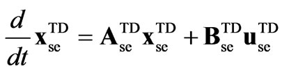 (18)
(18)
 ,
,  ,
,  ,
, 
where superscript TD denotes time domain modeling vectors and matrices.
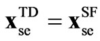
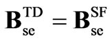
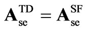
It should be noted that the SSSC TD representation in (18) has the same structure as the SF one in (14), which is to be expected since it is derived using the switching functions modeling. Differences arise when taking into account the coefficients in . The coefficients for the TD models considering harmonics are given in appendix B, for 12, 24 and 48-pulse VSC configurations.
In the same manner as for the SF models, the representation in (18) can be expressed in pu system as,
 (19)
(19)
 ,
,  ,
, 

 ,
,  ,
, 
 ,
, 
where subscript pu denotes variables and parameters in per unit system.
The coefficients of the TD models in pu for 12, 24 and 48-pulse arrangements are given in Appendix B.
Now, the TD STATCOM modeling is addressed based on the similarities with the SSSC models. The time domain models are derived using the equivalent circuit of Figure 6. Therefore, the STATCOM modeling is very similar to (18), except that the receiving end node voltages, vr, are zero.
Considering the differences between SSSC and STATCOM equivalent circuits, the TD modeling of the STATCOM becomes,
 (20)
(20)
 ,
,  ,
,  ,
, 
The STATCOM representation in (20) is very similar to the one in (18), except for vector ; also the variables and parameters for the TD SSSC models denoted by subscript se, are substituted for the STATCOM ones denoted by subscript sh.
The coefficients in  are the ones in
  for the 12, 24 and 48-pulse TD models, and are given in appendix B.
Similar to the SSSC modeling, (20) can be expressed in pu system as,
 (21)
(21)
 ,
,  ,
, 
The representation in (21) is very similar to the one in (19), except for vector ; also the variables and parameters for the SSSC models denoted by subscript se, are substituted for the STATCOM ones denoted by subscript sh. The pu variables and parameters are given in (19). The coefficients of the TD models in pu for 12, 24 and 48-pulse topologies are given in Appendix B.
4. Simulation Results
In order to assess the effectiveness and precision of the 24 and 48-pulse VSC models, comparison using the SF and TD models, and simulations carried out in Matlab/Simulink® are presented. Comparison is given for the SSSC SF and TD models only. Since SF and TD models represent the behavior of multi-pulse VSC’s and the difference between the FACTS devices presented in this paper is in their connection to the power system, generalization about the SF and TD models performance for the STATCOM is possible.
Simulations are carried out using the SSSC circuit shown in Figure 5 with the following parameters: R = 10 Ω, L = 700 mH, C = 2200 µF and three phase peak line voltages vs = Vm 30º and vr = Vm
 0º, Vm =
  kV, for a utility system frequency of 60Hz, resistances and inductances of the three phases are equal to R and L, respectively. The simulations presented suppose that the transient response has already passed and the steady state remains. No control is included in the system; in order to maintain the dc voltage magnitude, the appropriate VSC phase angle is used. The simulations consider dc capacitor voltages of approximately 25 kV and 12.5 kV for the 24 and 48-pulse VSC’s, respectively, and are carried out in the capacitive operating mode, which is the normal operating mode for a SSSC. All harmonic components are normalized in magnitude and frequency by the 60 Hz fundamental component.
The SSSC 24-pulse arrangement output and capacitor voltages are shown in the upper and lower graphs of Figure 7, respectively. It can be noticed that signals obtained using Matlab/Simulink®, as well as the SF and TD models show good agreement between them, and appropriately represent the switching behavior of the converter and its harmonic content. This is corroborated in Figure 8 where the harmonic components are depicted in the upper and lower graphs, respectively, for the SSSC output and capacitor voltages shown in Figure 7. The harmonic components and its magnitudes are comparable between them, which confirms the similarity of the output and capacitor voltage waveforms.
In the upper graph of Figure 7 harmonic distorted output voltage waveforms are shown that correctly represent the harmonic content present. In the lower graph of Figure 7 SSSC capacitor voltage waveforms are depicted, where the simulations using Matlab/Simulink®, as well as the SF and TD models are comparable between them, hence, properly representing the switching behavior of the SSSC.
The SSSC 48-pulse arrangement output and capacitor voltages are depicted in the upper and lower graphs of Figure 9, respectively. As in the case of the 24-pulse arrangement, the signals obtained using Matlab/Simulink®, as well as the SF and TD models show good agreement
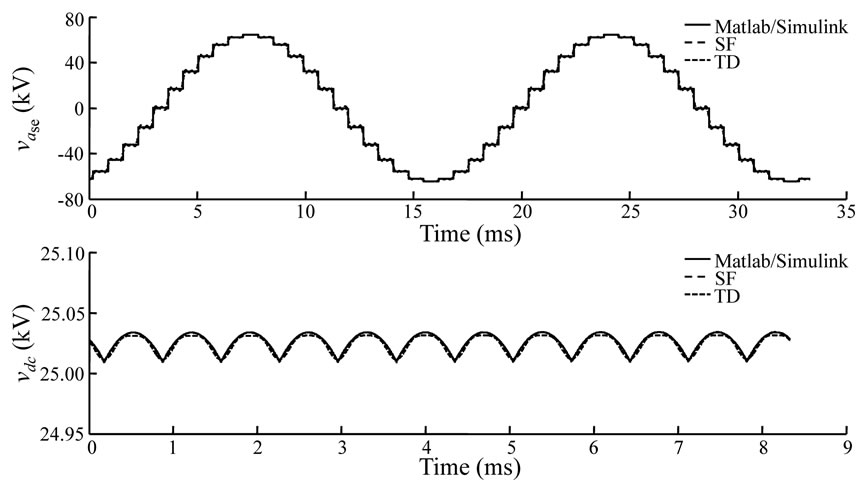
Figure 7. 24-pulse output and dc voltages
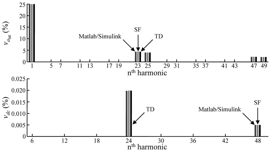
Figure 8. Harmonics of 24-pulse of output and dc voltages

Figure 9. 48-pulse output and dc voltages
between them. Figure 10 exhibits the harmonic components for the SSSC output and capacitor voltages shown in Figure 9, in the upper and lower graphs, respectively, which corroborates the similarities of the voltage waveforms. The harmonic components depicted in Figure 10 and its magnitudes are comparable between them.
Although signals using Matlab/Simulink® as well as the SF and TD models are very similar, the difference between them arises from variations in the simulations, e.g., in the SF and TD models, the turn-off devices and transformers are assumed to be ideal and lossless, unlike the components in Matlab/Simulink® where a small transformer reactance has to be included; discrepancy in the numerical methods also contributes to disparity between the signals. Furthermore, since the TD representation is a reduced order model, differences with the detailed simulations are expected; however, the TD models still correctly represent the harmonic components present in VSC signals.
Now, dynamic simulations comparing waveforms using the SF and TD models in pu system are carried out in order to assess the performance of the reduced TD models against the detailed SF ones.
For these dynamic simulations PI control systems are used in order to regulate active power flow over a transmission line.
The simulations are carried out in a system similar to the one illustrated in Figure 5, except that the impedance of each phase in composed of two branches in parallel, as depicted in Figure 11. The test circuit shows the arrangement for phase a where R1 = R2 = 0.0378 pu, XL1 = XL2 = 0.9978 pu, vs = Vsm 30° pu and vr = Vrm
 0° pu, Vsm = Vrm = 0.5774
 . Phases b and c are similar to a, except for phase shifted voltages. The frequency is 60Hz and the dc capacitor value is XC = 0.005pu. Simulations are carried out as follows; at the start of the simulation both impedance branches are connected, the dc capacitor voltage is zero and the reference value of the active power which the system has to reach is Pref = 0.52 pu. At t = 0.5 s one of the branches is disconnected from the system, leaving only R1 and XL1 connected. At t = 1 s the missing branch is reconnected, returning the system to its initial configuration. Finally, at t = 1.5 s the reference value of the active power changes to Pref = 0.72 pu.
The PI control gains are chosen as kp = 50 and Ti = 1 because of the fast response produced.
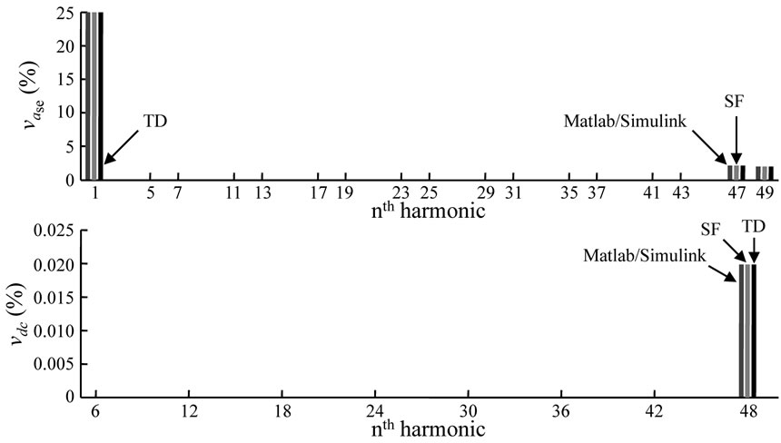
Figure 10. Harmonics of 48-pulse output and dc voltages

Figure 11. Test circuit of SSSC connected to a transmission line
The output and dc voltages of the 24-pulse converter are exhibited in Figure 12 for the SF and TD models. It can be seen from the waveforms that both simulations show comparable results. In order to compare these signals in more detail, a close-up is taken on two intervals of each waveform. Again, the waveforms show good agreement between them as illustrated in Figure 13.
Current and active power through the line are depicted in Figure 14, for the 24-pulse converter. The waveforms of the SF and TD simulations are comparable between them. Close-up intervals are also shown for both signals in Figure 15 which exhibit good agreement between them.
As for the 24-pulse converter, the output and dc voltages of the 48-pulse device are exhibited in Figure 16 for the SF and TD models. Again, close-up intervals are shown in Figure 17 for both signals resulting in comparable results between waveforms.
In addition, current and active power through the transmission line are depicted in Figure 18, for the 48-pulse converter SF and TD models. The waveforms of both simulations are comparable between them, which is confirmed in the close-up intervals presented for both signals in Figure 19.
The simulations presented show that in steady, as well as in transient state, the SF and TD models show good agreement between them, and can correctly represent the
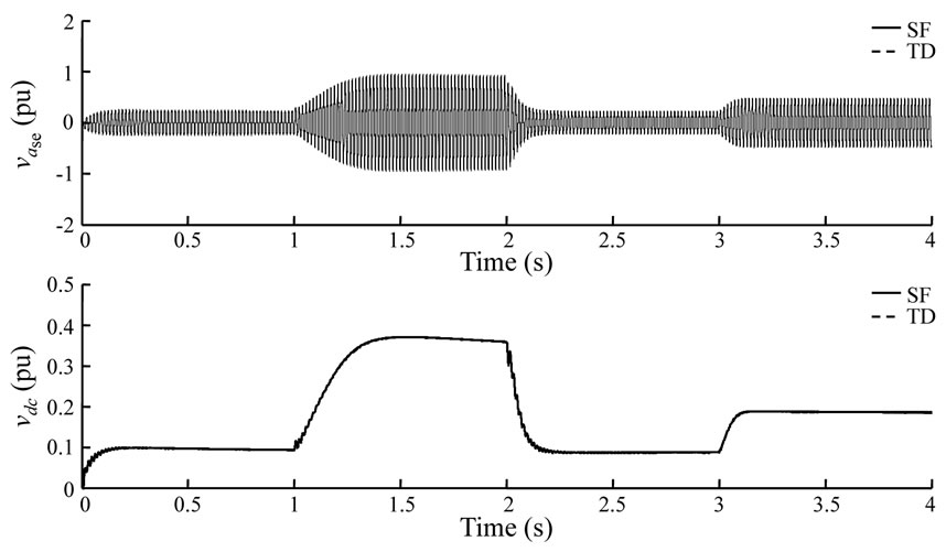
Figure 12. 24-pulse output and dc voltages

Figure 13. Close-up of 24-pulse output and dc voltages

Figure 14. 24-pulse current and active power
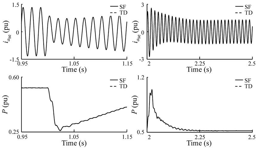
Figure 15. Close-up of 24-pulse current and active power

Figure 16. 48-pulse output and dc voltages
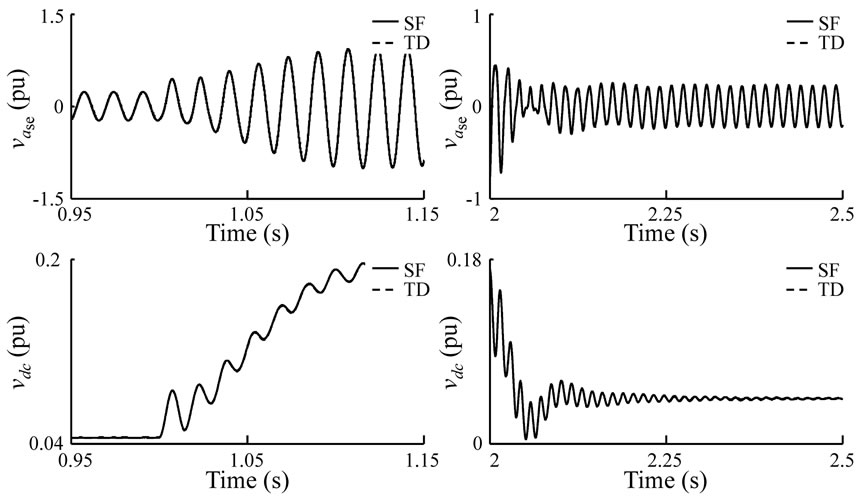
Figure 17. Close-up of 48-pulse output and dc voltages
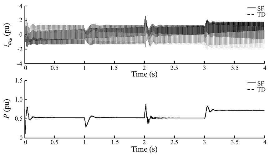
Figure 18. 48-pulse current and active power
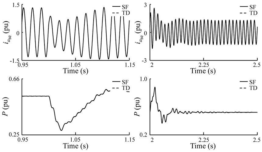
Figure 19. Close-up of 48-pulse current and active power
switching behavior of the multi-pulse converter arrangements.
Also, it is noteworthy to mention that as the number of pulses in the VSC configuration becomes higher, the TD modeling results in an A matrix with less elements, as opposed to the SF representation. Therefore, the TD is a much less complex modeling than the SF one in terms of calculation requirements. Since the SF is a detailed more complex representation, while the TD is a less complex one that still correctly represents VSC signals, the decision to use the SF or TD models is in relation to the level of detail and calculation requirements of the desired simulation.
5. Experimental Results
A laboratory implementation of a SSSC device is used for comparison of real and simulated signals in order to assess the SF and TD models performance.
The converter implementation consists of a dc voltage source, a GPP generator, two 6-pulse inverters, and a MCC. The implementation is divided in three stages: GPP generation, voltage inversion and output voltage development. Details of each stage are presented in Figure 20.
The GPP generation stage is based on an Atmel AT90S2313 microcontroller running at 10 MHz.
As depicted in Figure 20(a) the line current of phase a is used as a synchronization signal to coordinate the GPP

Figure 20. Diagrams of the (a) Gate pulse pattern generation, (b) Voltage inversion and (c) Output voltage development stages
of the commutating devices, and since it is a balanced inverter, phases b and c have a similar behavior, except that are phase shifted 120º and 240º, respectively. Due to this, the switching signals for phases b and c are also phase shifted.
The SSSC needs its output voltage synchronized in quadrature with the line current; in order for the synchronization to take place, the line current signal goes through a zero crossing detection sub-stage, which synchronizes the switching signals of the converter a branch with the line current of phase a. Once these signals are synchronized, the switching pattern can be phase shifted with respect to the synchronizing signal so as to have the desired performance. This synchronization is applied directly to one of the 6-pulse inverters; the other one has to be phase shifted 30º from the first one in order to generate the right 6-pulse voltages needed for the 12-pulse device.
Finally, the stage delivers a GPP with the correct phase shifting consisting of 12 switching signals, accommodated in two sets of six signals apiece, one for each 6-pulse VSC.
From a practical viewpoint the GPP generator stage acquires the current signal of phase a from a current sensor. This current signal enters a comparator circuit which sends an indication of the zero crossing events and its slope to a microcontroller. Once the slope and the occurrence of the zero crossings are determined, the microcontroller generates GPP’s like the one shown in Figure 2, with a delay time proportional to the phase shift angle desired.
The voltage inversion stage consists of the two 6-pulse inverters, each one generating a set of three phase ac voltages with the appropriate phase shift between them.
The three phase inverter bridges are accomplished using Powerex PS21353-GP modules. Each module consists of a three phase IGBT bridge, along with reverse diodes.
As shown in Figure 20(b) the two 6-pulse inverters have two inputs each one. The first input is a GPP, consisting of six switching signals coming from the GPP generation stage; the second one is a dc voltage.
Each inverter employs the appropriate gate signals to achieve three phase 6-pulse ac voltages using the dc voltage source. Both 6-pulse converters share the dc voltage source.
The GPP sets are fed to the 6-pulse inverter modules using optocouplers in order to optically isolate the logic and power circuits. Figure 21 depicts the prototype test system where two 6-pulse inverters are shown, each one of them has the configuration exhibited in Figure 1.
The output voltage construction stage consists of two three phase transformers arranged in the correct configuration. One of the transformers has a delta configuration with a turn ratio of , the other one has a star arrangement with a turn ratio of
 . The secondary sides of the two transformers are connected in series between them and with the test circuit transmission line. Figure 21 shows the arrangement of the MCC transformers and their connection with the test system.
As shown in Figure 20(c), the inputs of this stage are the two sets of three phase 6-pulse ac voltages generated by the voltage inversion process which using the MCC are combined to achieve three phase 12-pulse voltages that become the SSSC outputs.
The test circuit of the SSSC prototype is depicted in Figure 21 and is similar to the one from where the SF and TD models were derived. The circuit is comprised of two voltage sources named sending and receiving end three phase nodes. The angle of the two nodes is phase shifted to enable power transmission. A resistance, R, and an inductance, L, are included in order to represent test circuit line impedance. The three phase sinusoidal voltage source inserted in series with the line represents the SSSC voltage injections.
The test power system parameters are, R = 0.0165pu, XL = 0.1714 pu, the three phase ac voltages of the sending and receiving end nodes are respectively, vs = Vm 30°, and vr = Vm
 0°, where Vm = 0.5774
 pu. The system frequency is 60 Hz and the SSSC dc capacitor value is XC = 0.0014 pu.
The base values considered for power and voltage are, Pbase = 25 W and Vbase = 220 V, respectively.
Although the ratings of this laboratory implementation are not comparable in magnitude with those of an actual device, the system provides a basis from which to predict the behavior and performance of a much bigger installation. Furthermore, the verification of the SF and TD models can be directly applicable to higher rating devices.
Actual signals obtained from the laboratory prototype are compared with simulated signals achieved using the SF and TD models. All simulations are carried out using the test power system described with the parameters previously established. The comparison is accomplished in the capacitive mode of operation, since it is the normal operating mode for a SSSC. The current and voltage signals are all in per unit system.
The systems from which the actual SSSC and simulated signals are obtained suppose that the transient response has already passed and that the steady state remains. For the experiment, the magnitude of the SSSC dc voltage is 0.2045 pu.
The SSSC phase a line current and phase a output voltage are exhibited in Figure 22, in the upper and lower graphs, respectively. It can be noticed that the simulations using the SF and TD models, as well as the actual SSSC signals show comparable results. This helps to assess the effectiveness of the SF and TD models, since they adequately represent the switching behavior of the commutating devices in the power converter.
Besides, from the lower graph of Figure 22, each commutation in the multi-pulse simulated and actual

Figure 21. Prototype circuit of SSSC connected to a transmission line
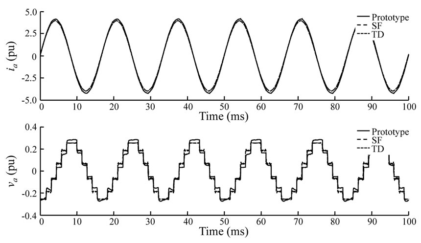
Figure 22. SSSC phase a line current and output voltage
waveforms show good agreement; therefore, switching of devices needed to achieve the output voltage are correctly represented.
The actual and simulated waveforms do not match exactly which can be due to several reasons. First of all, it is reasonable to think that simulated and experimental signals differ. Leaving aside the obvious, which are the assumptions made to derive the models and the differences in parameters, among the possible causes are the following. Since a 12-pulse SSSC configuration is balanced, differences in the values of the elements in each phase cause imbalance. Discrepancies in the magnetic coupling of each phase cause imbalance as well. The imbalance causes the converter not to work properly and, for instance, the MCC could not be achieving the exact construction of the simulated 12-pulse voltage for which it was designed.
Although the SF and TD models verification is made with a laboratory device rated at very small magnitudes compared to actual converter installations, the results obtained with the experiment can be extended to those higher rated systems.
Once the models have been validated, these can be included in simulations containing a diversity of equipment which would be hard to test or use in a laboratory. Also, several tests can be conducted in simulations using the models, which due to laboratory constraints would be very hard to perform in an actual experiment.
The SF modeling offers an accurate method of simulating multi-pulse based VSC devices, such as the SSSC and STATCOM, for studies in which the nature of the analysis demands it. However, although the TD representation is not a detailed model, but a reduced order one, it is accurate enough to correctly represent the harmonic components present in the VSC signals.
The prototype is a 12-pulse VSC due to a higher topology signifies an increase in the device elements, like components or transformers, which represents much higher cost.
Although the models verified are 12-pulse ones, the results can be extended to higher pulse models like the 24 or 48-pulse SF and TD models in order to predict their precision and performance.
6. Conclusions
The paper presents the derivation of multi-pulse VSC based SF and TD models. The models are then compared with Matlab/Simulink® simulations showing good results.
The SF models are intended to represent in detail the behavior of multi-pulse VSC devices, maintaining a compromise between complexity and accuracy. On the other hand, TD models are reduced representations that enable good performance of multi-pulse VSC based FACTS, combined with less calculation requirements than the SF models.
A laboratory prototype was constructed to compare the signals generated with the 12-pulse SF and TD models in order to assess their performance. The comparison of the signals shows adequate results.
Since the effectiveness and precision of the models have been verified and show good results, these can furthermore be included in power system studies where detailed representations of SSSC and STATCOM devices are needed.
REFERENCES
- S. Mori, K. Matsuno, M. Takeda, M. Seto, T. Hasegawa, S. Ohnishi, S. Murakami, and F. Ishiguro, “Development of a large static VAR generator using self-commutated inverters for improving power system stability,” IEEE Transactions on Power Systems, Vol. 8, No. 1, pp. 371– 377, February 1993.
- C. Schauder, M. Gernhardt, E. Stacey, T. Lemak, L. Gyugyi, T. W. Cease, and A. Edris, “Development of a ±100 MVAR static condenser for voltage control of transmission systems,” IEEE Transactions on Power Delivery, Vol. 10, No. 3, pp. 1486–1493, July 1995.
- C. Schauder, “The unified power flow controller—A concept becomes reality,” IEE Colloquium: Flexible AC Transmission Systems—The FACTS, Vol. 1998, No. 500, pp. 7–12, November 1998.
- K. K. Sen, “SSSC – Static synchronous series compensator: Theory, modeling, and applications,” IEEE Transactions on Power Delivery, Vol. 13, No. 1, pp. 241–246, January 1998.
- L. S. Kumar and A. Ghosh, “Modeling and control design of a static synchronous series compensator,” IEEE Transactions on Power Delivery, Vol. 14, No. 4, pp. 1448– 1453, October 1999.
- D. Soto and T. C. Green, “A comparison of high-power converter topologies for the implementation of FACTS controllers,” IEEE Transactions on Industrial Electronics, Vol. 49, No. 5, pp. 1072–1080, October 2002.
- A. Nabavi-Niaki and M. R. Iravani, “Steady-state and dynamic models of unified power flow controller (UPFC) for power system studies,” IEEE Transactions on Power Systems, Vol. 11, pp. 1937–1943, November 1996.
- K. R. Padiyar and A. M. Kulkarni, “Design of reactive current and voltage controller of static condenser,” Electrical Power & Energy Systems, Vol. 19, No. 6, pp. 397– 410, August 1997.
- R. Mihalic and I. Papic, “Static synchronous series compensator-a mean for dynamic power flow control in electric power systems,” Electric Power Systems Research, Vol. 45, No. 1, pp. 65–72, April 1998.
- A. Sonnenmoser and P. W. Lehn, “Line current balancing with a unified power flow controller,” IEEE Transactions on Power Delivery, Vol. 14, No. 3, pp. 1151–1157, July 1999.
- I. Papic, “Mathematical analysis of FACTS devices based on a voltage sourced converter Part 1: Mathematical models,” Electric Power Systems Research, Vol. 56, No. 2, pp. 139–148, November 2000.
- P. García-González and A. G. Cerrada, “Detailed analysis and experimental results of the control system of a UPFC,” IEE Proceedings of Generation, Transmission and Distribution, Vol. 150, No. 2, pp. 147–154, March 1996.
- N. G. Hingorani and L. Gyugyi, “Understanding FACTS: Concepts and technology of flexible. AC transmission systems,” IEEE Press, 1999.
- M. Mohaddes, A. M. Gole, and Sladjana Elez, “Steady state frequency response of STATCOM,” IEEE Transactions on Power Delivery, Vol. 16, No. 11, pp. 18–23, January 2001.
- P. Zúñiga-Haro and J. M. Ramírez, “Multipulse VSC based SSSC,” Proceedings of 2008 IEEE Power Engineering Society General Meeting, Pittsburgh, pp. 1–8, 2008.
- P. Zúñiga-Haro and J. M. Ramírez, “Static synchronous series compensator operation based on 48-pulse VSC,” Proceedings of 2005 IEEE Power Engineering Society 37th Annual North American Power Symposium, pp. 102–109, 2005.
Appendix A
12, 24 and 48-pulse SF models coefficients 12-pulse SF model coefficients.
 ,
, 
 ,
, 
 ,
, 
where i=1.
24-pulse SF model coefficients.


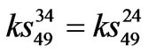
48-pulse SF model coefficients.


The superscripts 12, 24 and 48 denotes 12, 24 and 48-pulse SF models coefficients, respectively; subscripts Y-Y and Δ-Y correspond to the configuration of the coupling transformer of each VSC in the multi-pulse configuration as detailed in [15, 16], and the coefficients elements are given by,


 ,
, 
Appendix B
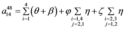
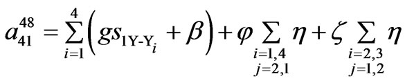
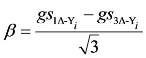
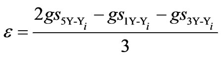
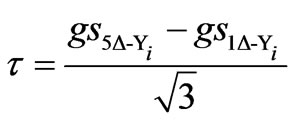
12, 24 and 48-pulse TD models coefficients 12-pulse TD model coefficients.


where,
 ,
,  ,
,  ,
, 
 ,
,  ,
,  ,
, 
 ,
,  ,
,  ,
, 
 ,
,  ,
,  ,
, 
 ,
,  ,
, 
 ,
,  ,
,  ,
, 
 ,
,  ,
, 
 ,
,  ,
, 
 ,
,  ,
, 
 ,
,  ,
, 
 ,
,  ,
, 
 ,
,  ,
,  ,
, 
 ,
,  ,
,  ,
, 
 ,
,  ,
,  ,
, 
 ,
,  ,
,  ,
, 
 ,
,  ,
, 
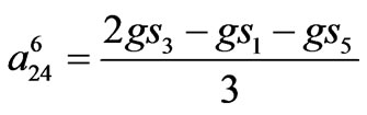
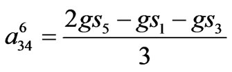
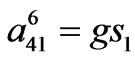
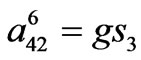
Coefficients a41, a42 and a43 have the same structure as a14, a24 and a34, respectively, except that constants k014, k024 and k034 are equal to 1/2.
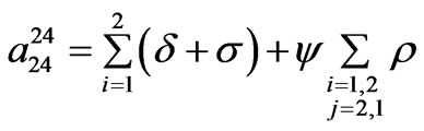
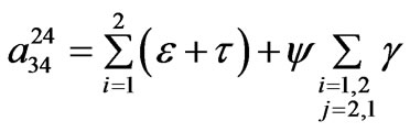
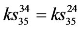
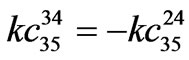
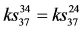
24-pulse TD model coefficients.


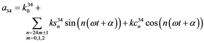
where,
 ,
,  ,
,  ,
, 
 ,
,  ,
,  ,
, 
 ,
,  ,
, 
 ,
,  ,
,  ,
, 
 ,
,  ,
, 
 ,
,  ,
, 
 ,
,  ,
,  ,
, 
 ,
,  ,
,  ,
, 
 ,
,  ,
, 
Coefficients a41, a42 and a43 have the same structure as a14, a24 and a34, respectively, except that constants k014, k024 and k034 are equal to 1.
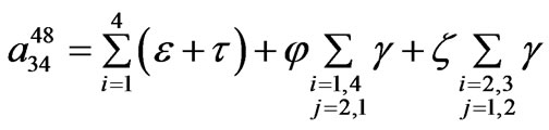
48-pulse TD model coefficients.


where,
 ,
,  ,
,  ,
, 
 ,
,  ,
, 
 ,
,  ,
,  ,
, 
 ,
,  ,
, 
 ,
,  ,
,  ,
, 
 ,
,  ,
, 
Coefficients a41, a42 and a43 have the same structure as a14, a24 and a34, respectively, except that constants k014, k024 and k034 are equal to 2.
NOTES
This work was supported in part by PROMEP under grant 103.5/09/1420.