Journal of Electromagnetic Analysis and Applications
Vol. 3 No. 7 (2011) , Article ID: 5909 , 10 pages DOI:10.4236/jemaa.2011.37045
New Control Algorithm for Capacitor Supported Dynamic Voltage Restorer
![]()
1Department of Electrical Engineering, Indian Institute of Technolog, Delhi, India; 2Government College of Engineering, Kannur, India; 3Vellore Institute of Technology, Vellore, India; 4Department of Electrical Engineering, Êcole de Technologie Superieure, Universite du Quebec, Montreal, Canada.
Email: bsingh@ee.iitd.ac.in, jayaprakashpee@gmail.com, dpk0710@yahoo.com, ambrish.chandra@etsmtl.ca, kamal.al-haddad@etsmtl.ca
Received April 1st, 2011; revised May 2nd, 2011; accepted May 27th, 2011.
Keywords: Power quality, distribution system, dynamic voltage restorer, voltage source converter, indirect control
ABSTRACT
In this paper, a simple control algorithm for the dynamic voltage restorer (DVR) is proposed to mitigate the power quality problems in terminal voltage such as sag, swell, harmonics, unbalance etc. Two PI (proportional-integral) controllers are used each to regulate the dc bus voltage of DVR and the load terminal voltage respectively. The fundamental component of the terminal voltage is extracted using the synchronous reference frame theory. The control signal for the series connected DVR is obtained indirectly from the extracted reference load terminal voltage. The proposed DVR control strategy is validated through extensive simulation studies using MATLAB software with its Simulink and Simpower system (SPS) block set tool boxes.
1. Introduction
Power quality issues in the distribution system are widely addressed in the literature [1-9] due to the sensitive and critical loads such as precise manufacturing plants, automation etc. A new group of devices based on PWM (Pulse Width Modulated) switching solid state compensators are developed and used for improving power quality in the distribution system under the generic name of custom power devices [3,7]. They are mainly of three categories such as shunt connected distribution static compensator (DSTATCOM), series connected compensator like dynamic voltage restorer (DVR) and unified power quality conditioner (UPQC) which is connected in both shunt and series with the ac mains. The series connected compensator can regulate the load terminal voltage from the “low quality” terminal voltage and protect the critical consumer loads from tripping and consequent loss. The installation of custom power devices at the consumer point is governed by the IEEE standard [10].
A DVR is connected between the supply and the sensitive load so that it can inject a voltage of required waveform. Hence it can protect sensitive consumer loads from supply disturbances. In a capacitor supported DVRthe power absorbed/supplied is almost zero except small losses in the steady state and the voltage injected by the DVR should be in quadrature with the feeder current [3]. The analysis, design and voltage injection schemes of DVR is discussed in the literature [11-17] and the different control strategies are developed in [18-22]. The instantaneous reactive power theory (IRPT) [6], sliding mode controller based [14], symmetrical components based [15] control techniques for series compensators are reported in the literature.
The SRFT (synchronous reference frame theory) based algorithm reported in [21] has the advantage that the calculation is performed in the rotating reference frame. But, the computation involves conversion from stationary frame to rotating frame and then the reference signals from rotating frame to stationary frame. The IRPT algorithm [6] for the reference signal generation involves the conversion from three-phase to two-phase and vice versa. A new control algorithm is developed based on unit templates for the control of a capacitor supported DVR for compensation of voltage sag, swell, harmonics and unbalance in terminal voltage [23]. In this paper, the algorithm is discussed in detail and it is improved by using a PLL (phase locked loop) to extract fundamental component of the terminal voltage. The design of ripple filter is also investigated for improving the performance of a DVR system. Extensive simulations are performed using MATLAB software with its Simulink and SimPower System (SPS) tool boxes for verifying the proposed control algorithm of DVR.
2. Principle of Operation of DVR
The schematic diagram of a capacitor supported DVR is shown in Figure 1. Three voltage sources (vsa, vsb, vsc) represent a 3-phase three-wire supply system and the series source impedances are shown as Za (La, Ra), Zb (Lb, Rb) and Zc (Lc, Rc). The DVR uses a transformer (Tr) to inject a voltage in series with the terminal voltage. A voltage source converter (VSC) along with a dc capacitor (Cdc) is used as a DVR. The ripple in the injected voltage is filtered using a series inductor (Lr) and a parallel capacitor (Cr). The load considered is a three phase lagging power factor load.
The ripple filter is designed based on the switching frequency (fs). It is designed such that the capacitor (Cr) offers a low impedance path for the switching ripple and the series inductor (Lr) provides high impedance for the switching ripple. The reactance given by the capacitor (Cr) and inductor (Lr) at half of the switching frequency (5 kHz) for fs = 10 kHz i.e., fr = fs/2 is calculated as
XCr = 1/(2*π* fr *Cr) = 1/(2*3.14*5000*Cr)(1)
XLr = 2*π* fr *Lr = 2*3.14*5000*Lr.(2)
Considering, XCr = 3 Ω, Cr = 10.61 μF and XLr = 100 Ω, Lr = 3.18 mH. These values of ripple filter elements are initially used for simulation and by iteration it is found that, Lr= 3.5 mH and Cr = 10 μF are suitable for minimum ripple in the output of DVR.
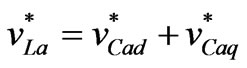
Figure 2 shows the phasor diagram of the DVR operation for the compensation of sag in the terminal voltage. The load terminal voltage and current during pre-sag condition are represented as VL(presag) and IL’. After the sag event, the terminal voltage (Vt) is of lower in magnitude that of pre-sag condition. The voltage injected by the DVR (Vc) is used to maintain the load voltage (VL) at the rated magnitude and this has two components, Vcd and Vcq. The voltage in-phase with the current (Vcd) is to regulate the dc bus voltage of DVR and also to meet the power loss in the DVR. The voltage in quadrature with the current (Vcq) is to regulate the load voltage (VL) at constant magnitude. The aim of the control algorithm is to achieve these two components of the injection voltage. The sag, swell, harmonic and unbalance in terminal voltage are also compensated by the proposed DVR through extracting the required reference load voltage.
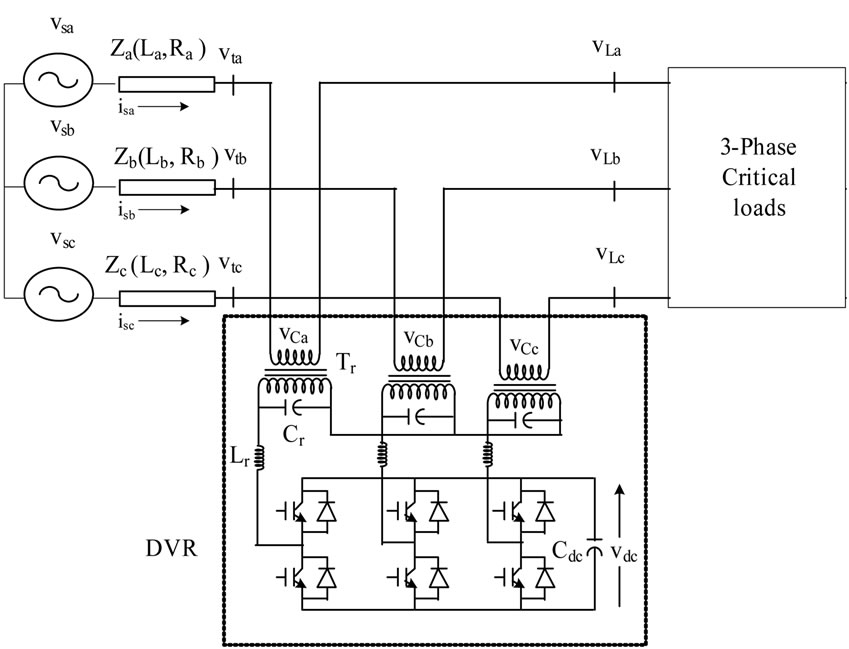
Figure 1. Schematic diagram of capacitor supported DVR for power quality improvement.
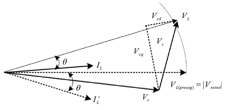
Figure 2. Phasor diagram of capacitor supported DVR.
3. Control Strategy of DVR
The proposed control algorithm is derived from the algorithm presented in [18] in which the shunt compensator is controlled for harmonic current compensation, load current balancing and power factor correction. Here, the sag, swell, harmonic voltage and unbalance in terminal voltage are compensated by controlling the DVR. The load terminal voltage is regulated and the waveform is controlled to sinusoidal. The proposed control scheme is shown in Figure 3.
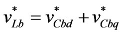
The reference load terminal voltages ( ,
, ,
, ) are derived from the sensed supply currents (iSa, iSb, iSc), terminal voltages (vta, vtb, vtc) and the dc bus voltage (vdc) of DVR as feedback signals. There are two proportionalintegral (PI) controllers used to regulate the dc bus voltage of DVR and to regulate the load voltage (vL).
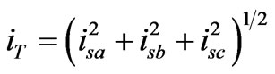
Three phase in-phase unit voltage templates (ua, ub, uc) are derived from the supply currents (iSa, iSb, iSc) as,
 (3)
(3)
ua = isa/iT; ub = isb/iT; uc = isc/iT; (4)
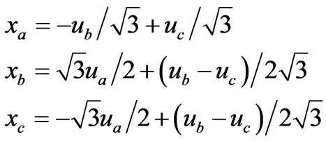
Moreover, the quadrature unit vectors (xa, xb, xc) are derived from the in-phase unit vectors as,
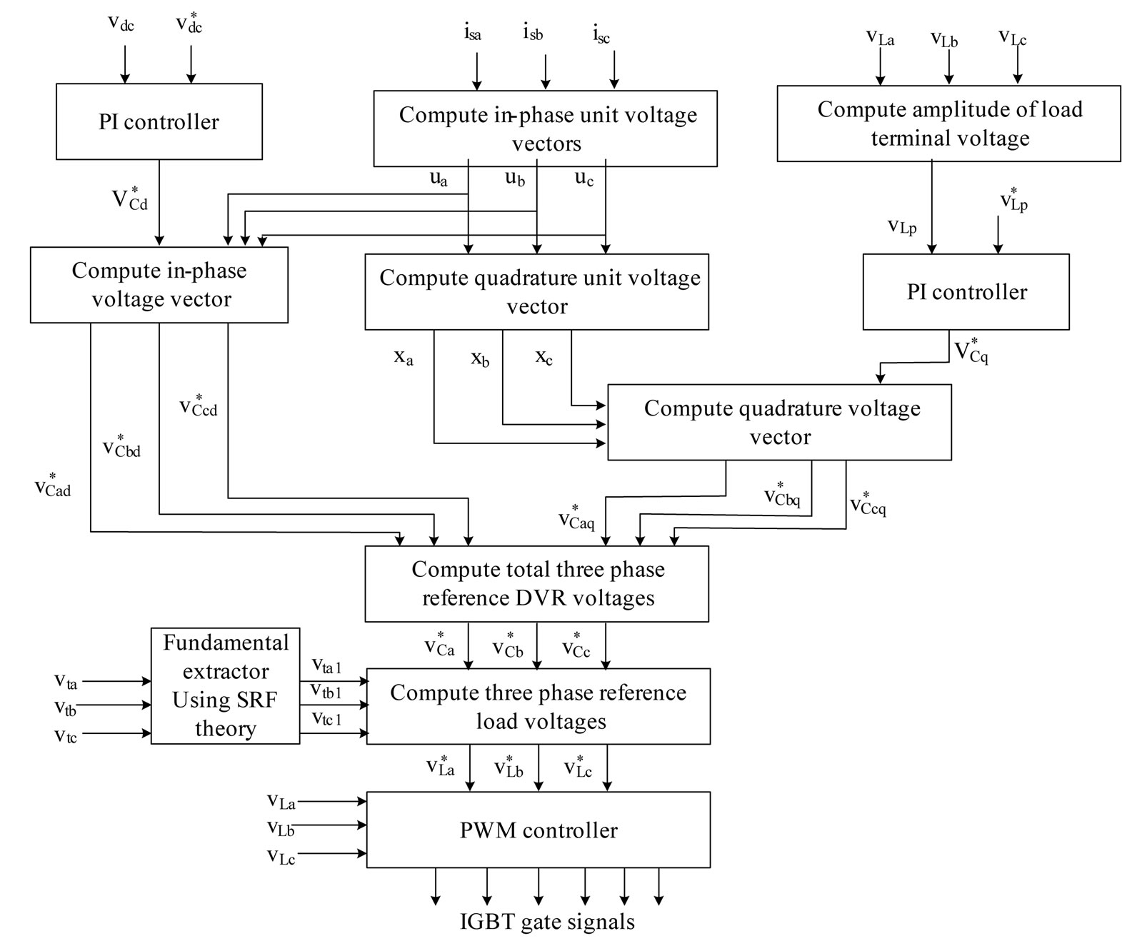
Figure 3. Control scheme of the DVR for power quality improvement.
 (5)
(5)
The dc bus voltage of the DVR is regulated using a PI controller over the sensed (vdc) and reference values ( ) of dc bus voltage. This PI controller output is considered as the amplitude (
 ) of the in-phase component of the injection voltages (
 *,
*, ,
, ) as,
) as,
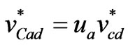 (6)
(6)
 (7)
(7)
 (8)
(8)
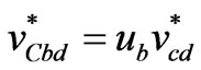
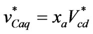
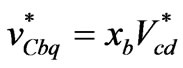
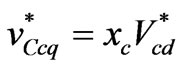
A second PI controller is used to derive the amplitude ( ) of the quadrature component of the injection voltages (
 ,
, ,
, ) of the DVR by using it over the amplitude of sensed load voltage (VLp) and reference value (
 ) of the load terminal voltage as,
 (9)
(9)
 (10)
(10)
 (11)
(11)
To estimate the positive sequence fundamental component of terminal voltages (vta1, vtb1, vtc1), the sensed terminal voltages (vta, vtb, vtc) are required. Two phase unit voltage vectors are derived using a PLL (phase locked loop) over the terminal voltage. The fundamental component of the terminal voltages (vta1, vtb1, vtc1) are extracted from the sensed terminal voltages (vta, vtb, vtc) using the synchronous reference frame (SRF) transformation [21]. The reverse of the SRF transformation after filtering the dc component gives the fundamental component of the terminal voltage.
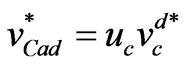
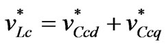
The algebraic sum of the in-phase components ( ,
,  ,
, ), the quadrature components (
 ,
,  ,
, ) and the fundamental of terminal voltages (vta1, vtb1, vtc1) are taken as the reference load voltages (
 ,
,  ,
, ) as,
) as,
 (12)
(12)
 (13)
(13)
 (14)
(14)
A pulse width modulated (PWM) controller is used over the reference ( ,
,  ,
, ) and sensed load voltages (vLa, vLb, vLc) to generate gating signals for the IGBT’s (Insulated Gate Bipolar Transistors) of the DVR. The carrier wave (triangular) frequency is set at 10 kHz. The gating pulses switch the IGBT’s of the DVR for the compensation of sag, swell, unbalance and harmonics in terminal voltage.
4. MATLAB Based Simulation of the System
Figure 4 shows the MATLAB model of the DVR connected system. The terminal voltage is realized by using a three-phase voltage source and the source impedance is connected in its series. In order to simulate the disturbances at the PCC voltage, an additional load is switched on with a circuit breaker. The load considered is a lagging power factor load. The DVR is connected in series with the supply using an injection transformer. The VSC is connected to the transformer along with a ripple filter. The dc bus capacitor is selected based on the transient energy requirement and the dc bus voltage is selected based on the injection voltage level. The dc capacitor decides the ripple content in the dc voltage. The considered system data are given in Appendix.
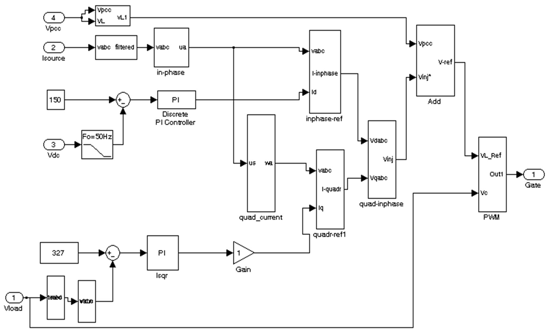
The control algorithm for the DVR is modeled in MATLAB and is given in Figure 5(a). The control scheme shown in Figure 3 is modeled using the tools available in Simulink of MATLAB environment. The fundamental of terminal voltage is extracted using synchronous reference frame theory and the model developed is shown in Figure 5(b). The reference load terminal voltages are derived from the sensed terminal volt-ages, supply currents, load terminal voltages and the dc bus voltage of DVR. A pulse width modulation (PWM) controller is used over the reference and sensed load
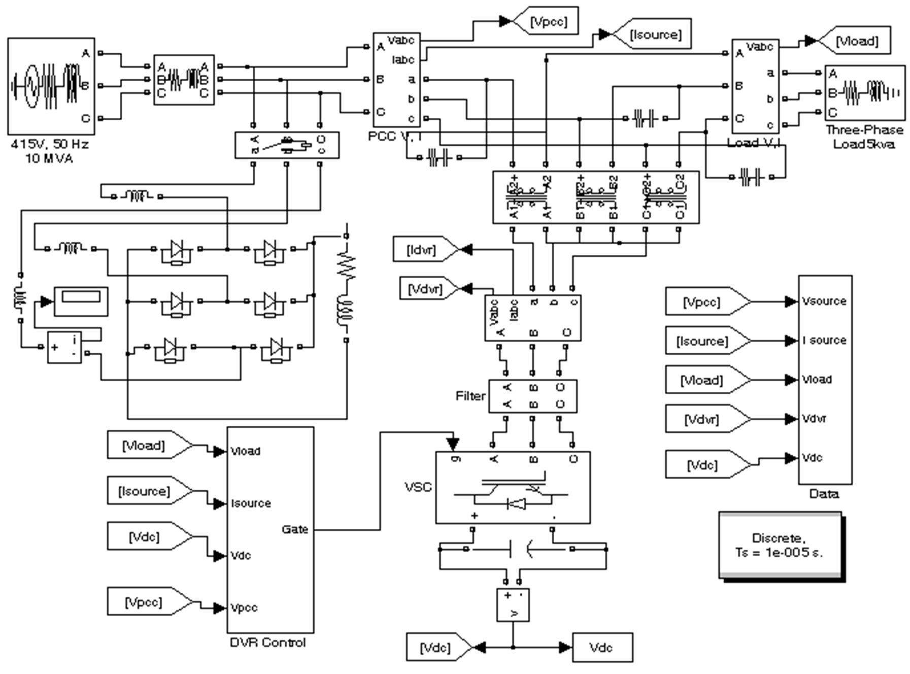
Figure 4. MATLAB model of the DVR connected system.
 (a)
(a)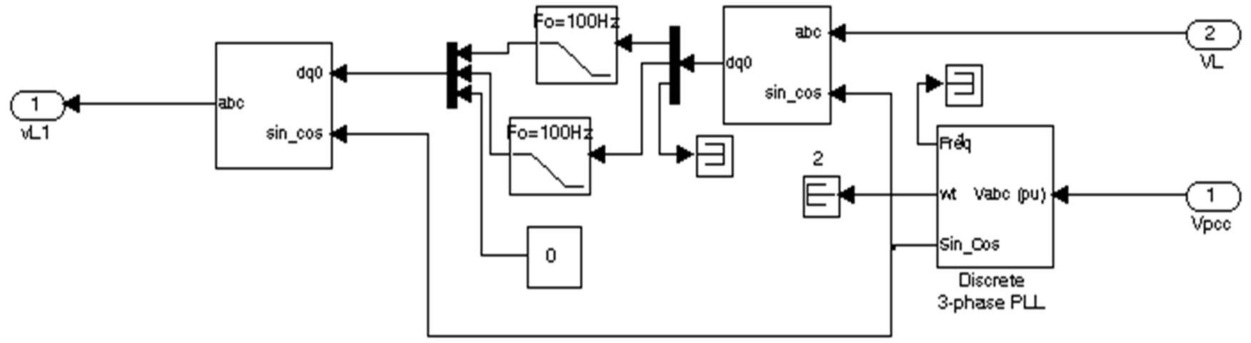 (b)
(b)
Figure 5. (a) MATLAB model of the control scheme of DVR (b) Subsystem for fundamental terminal voltage extraction using SRF theory.
voltages to generate gating signals for the IGBT’s (Insulated Gate Bipolar Transistors) of the DVR.
5. Performance of the System
The performances of the DVR for different supply disturbances are tested under various operating conditions. The proposed control algorithm is tested for different power quality events like voltage sag (Figure 6), voltage swell (Figure 7), unbalance in terminal voltages (Figure 8) and harmonics in terminal voltages (Figure 9). Figure 6 shows balanced sag of 30% in terminal voltage at 0.15 s and occurs for 5 cycles of ac mains. The DVR injects funda mental voltage (vc) in series with the terminal voltage (vt). The load voltage (vL) is regulated at the rated value. The supply current (is), amplitude of terminal voltage (VSp), the amplitude of load voltage (VLp) and the dc bus voltage (vdc) are also shown in Figure 6.
The dynamic performance of the DVR for a swell in terminal voltage is given in Figure 7. The load voltage (vL) is regulated at rated value, which shows the satisfactory performance of the DVR. The supply current (is), the amplitude of load voltage (VLp), the amplitude of terminal voltage (Vtp) and the dc bus voltage (vdc) are also shown in the Figure 7. The dc bus voltage is regulated at
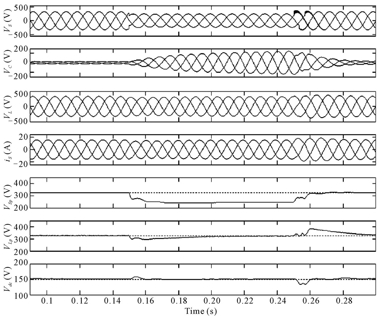
Figure 6. Compensation of PCC voltage sag using DVR.
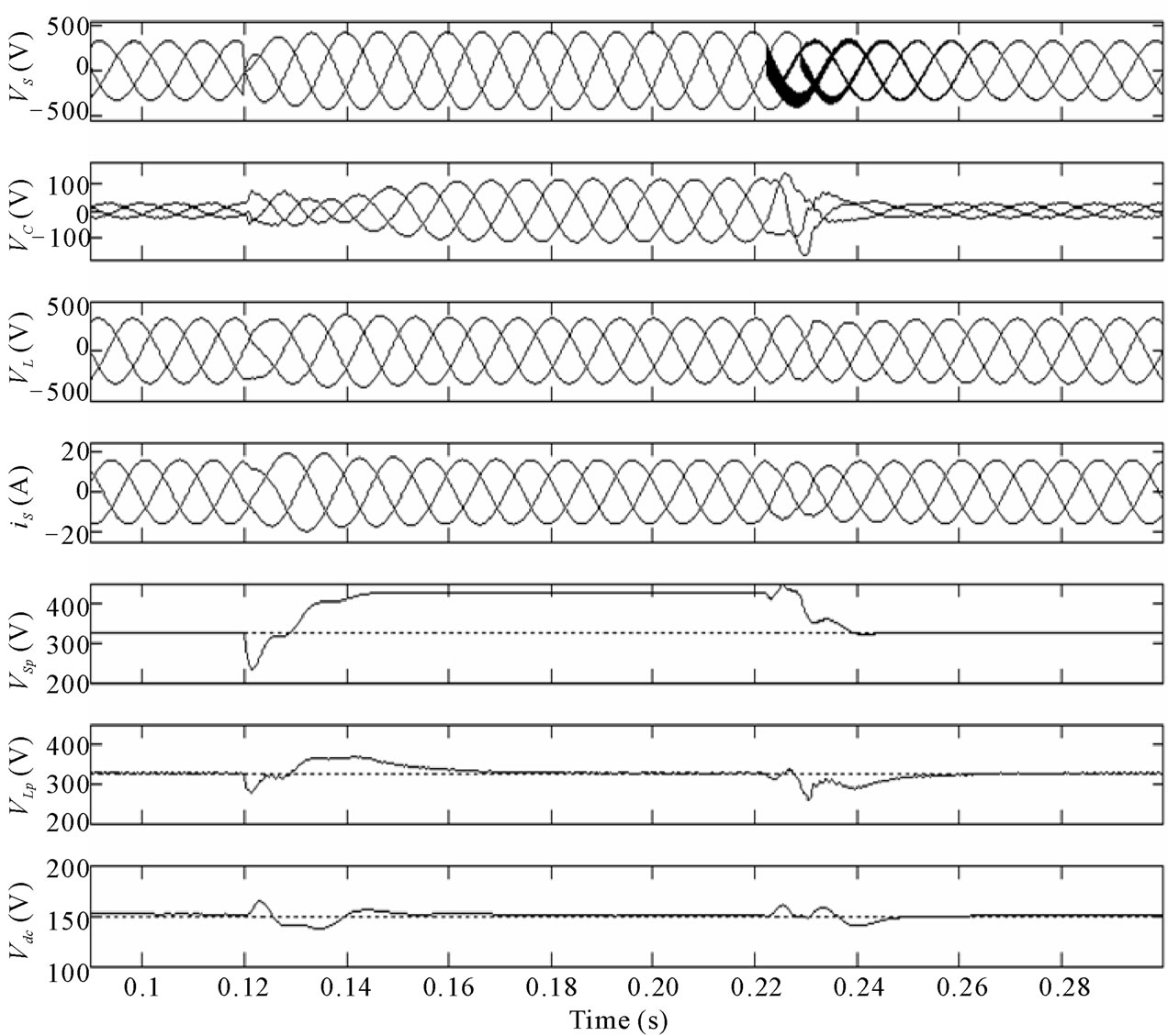
Figure 7. Compensation of supply voltage swell using DVR.
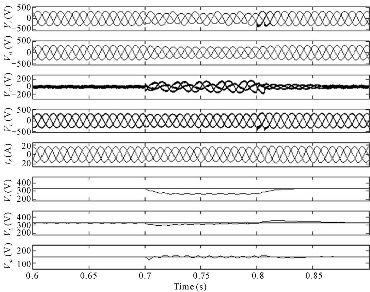
Figure 8. Compensation of supply voltage unbalance using DVR.
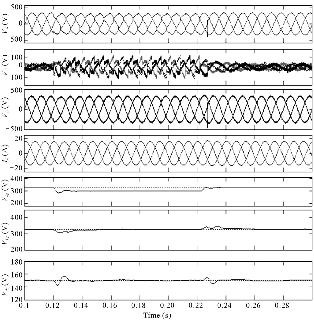
Figure 9. Compensation of supply voltage harmonics using DVR.
the reference value, though small fluctuations occur during transients.
The performance of DVR for an unbalance in terminal voltages is shown in Figure 8. The phase voltages at the PCC are different in magnitude at 0.7 s as given in the voltage at PCC (vt) of Figure 8. Now, the DVR injects unequal fundamental voltages (vc) so that the load voltage (vL) is regulated to constant magnitude. The supply current (is), the amplitude of load voltage (VLp), the amplitude of terminal voltage (Vtp) and the dc bus voltage (vdc) are also shown in Figure 8 to demonstrate the satisfactory behavior of DVR.
The harmonics compensation in terminal voltage is tested and depicted in Figure 9. The voltage at PCC (vt) is distorted and the load voltage (vL) is undistorted and constant in magnitude due to the injection of harmonic voltage (vc) by the DVR. The load terminal voltage (vL) has a total harmonic distortion (THD) of 1.2% (Figure 10) at the time of disturbance and the voltage at PCC has a THD of 7.33% (Figure 11). The supply current is also sinusoidal with a THD of 0.14% (Figure 12).
6. Conclusions
A new control algorithm based on proportional-integral controllers has been proposed for a capacitor supported dynamic voltage restorer. The proposed algorithm is based on the estimation of in-phase and quadrature component of injection voltages using two PI controllers each for regulating the dc bus voltage of DVR and the load voltage respectively. The reference voltages for the DVR have been obtained indirectly by extracting the reference load terminal voltage. The proposed control algorithm of
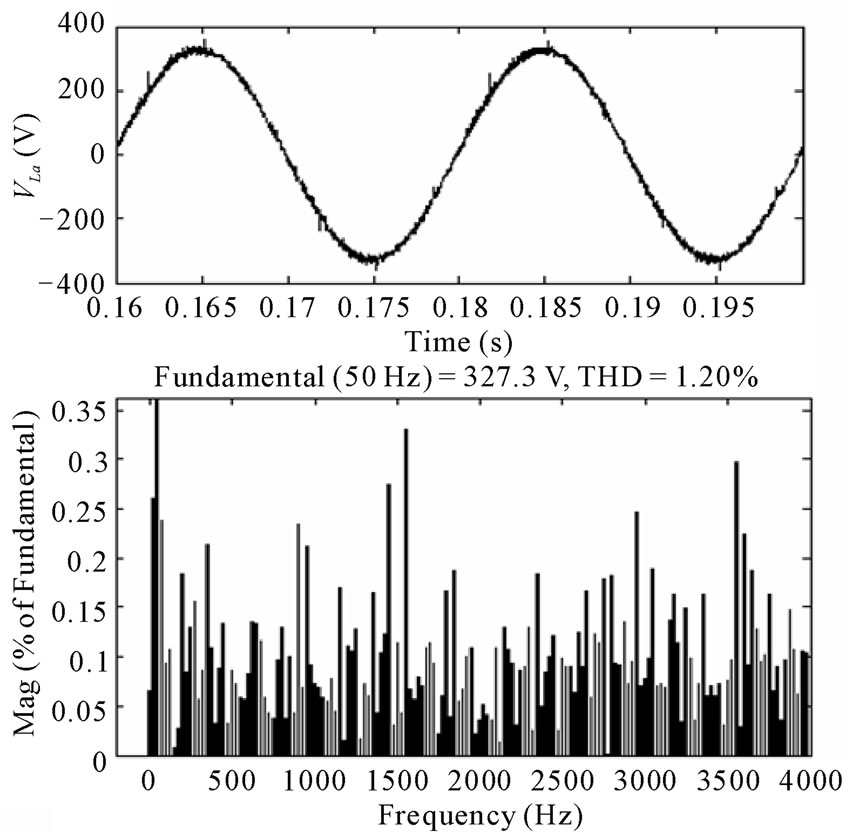
Figure 10. Load voltage along with harmonic spectrum.
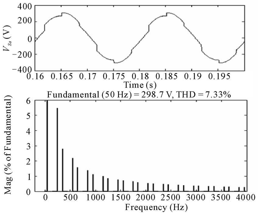
Figure 11. Voltage at PCC along with harmonic spectrum.
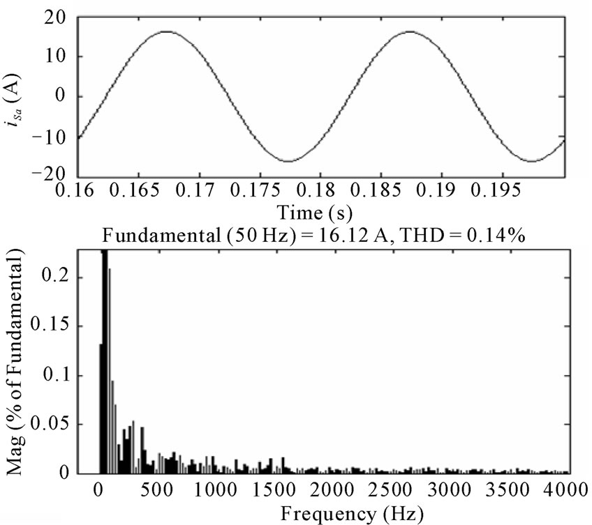
Figure 12. Supply current along with harmonic spectrum.
DVR has been validated through simulation using MATLAB software along with simulink and Simpower system (SPS) toolboxes. The performance of the DVR has been observed to be satisfactory for various power quality disturbances like sag, swell, unbalance and harmonics in PCC voltages. Moreover, it is able to provide a self-supported dc bus of the DVR through power transfer from ac line at fundamental frequency.
REFERENCES
- M. H. J. Bollen, “Understanding Power Quality Problems Voltage Sags and Interruptions,” IEEE Press, New York, 2000.
- J. Schlabbach, D. Blume and T. Stephanblome, “Voltage Quality in Electrical Power Systems,” The Institution of Engineering and Technology, Stevenage, 2000.
- A. Ghosh and G. Ledwich, “Power Quality Enhancement Using Custom Power Devices,” Kluwer Academic Publishers, London, 2002.
- R. C. Dugan, M. F. McGranaghan and H. W. Beaty, “Electric Power Systems Quality,” 2nd Edition, McGraw Hill, New York, 2006.
- A. Moreno-Munoz, “Power Quality: Mitigation Technologies in a Distributed Environment,” Springer-Verlag London limited, London, 2007.
- H. Akagi, E. H. Watanabe and M. Aredes, “Instantaneous Power Theory and Applications to Power Conditioning,” John Wiley & Sons, Hoboken, 2007. doi:10.1002/0470118938
- K. R. Padiyar, “FACTS Controllers in Transmission and Distribution,” New Age International, New Delhi, 2007.
- E. F. Fuchs and M. A. S. Mausoum, “Power Quality in Power Systems and Electrical Machines,” Elsevier Academic Press, London, 2008.
- A. Baggini, “Handbook on Power Quality,” John Wiley & Sons, Hoboken, 2008. doi:10.1002/9780470754245
- IEEE Standards Office, “lEEE Recommended Practices and Requirements for Harmonics Control in Electric Power Systems,” IEEE Standards 519-1992, 1992.
- M. Vilathgamuwa, R. Perera, S. Choi and K. Tseng, “Control of Energy Optimized Dynamic Voltage Restorer,” Industrial Electronics Society’99 Proceedings, Vol. 2, 1999, pp. 873-878.
- I.-Y. Chung, D.-J. Won, S.-Y. Park, S.-I. Moon and J.-K. Park, “The DC Link Energy Control Method in Dynamic Voltage Restorer System,” International Journal of Electrical Power & Energy Systems, vol. 25, no. 7, 2003, pp. 525-531. doi:10.1016/S0142-0615(02)00179-5
- A. Moreno-Munoz, D. Oterino, M. Gonzalez, F. A. Olivencia and J. J. Gonzalez-de-la-Rosa, “Study of Sag Compensation with DVR,” Proceedings of IEEE MELECON, Benalmadena, Malaga, 16-19 May 2006, pp 990-993.
- B. N. Singh, A. Chandra, K. Al-Haddad and B. Singh, “Performance of Sliding-Mode and Fuzzy Controllers for a Static Synchronous Series Compensator,” IEE Proceedings on Generation, Transmission and Distribution, vol. 146, no. 2, March 1999, pp. 200-206. doi:10.1049/ip-gtd:19990072
- A. Ghosh, A. K. Jindal and A. Joshi, “Design of a Capacitor-Supported Dynamic Voltage Restorer (DVR) for Unbalanced and Distorted Loads,” IEEE Transactions on Power Delivery, vol. 19, no. 1, 2004, pp. 405-413. doi:10.1109/TPWRD.2003.820198
- M. R. Banaei, S. H. Hosseini, S. Khanmohamadi and G. B. Gharehpetian, “Verification of a New Energy Control Strategy for Dynamic Voltage Restorer by Simulation,” Simulation Modelling Practice and Theory, vol. 14, no. 2, 2006, pp. 112-125. doi:10.1016/j.simpat.2005.03.001
- M. R. Banaei, S. H. Hosseini and G. B. Gharehpetian, “Inter-Line Dynamic Voltage Restorer Control Using a Novel Optimum Energy Consumption Strategy,” Simulation Modelling Practice and Theory, vol. 14, no. 7, 2006, pp. 989-999. doi:10.1016/j.simpat.2006.06.001
- A. Chandra, B. Singh, B. N. Singh and K. AI-Haddad, “An Improved Control Algorithm of Shunt Active Filter for Voltage Regulation, Harmonic Elimination, PowerFactor Correction, and Balancing of Nonlinear Loads,” IEEE Transactions on Power Electronics, vol. 15, no. 3, May 2000, pp. 495-507. doi:10.1109/63.844510
- A. K. Jindal, A. Ghosh and A. Joshi, “Critical Load Bus Voltage Control Using DVR under System Frequency Variation,” Electric Power Systems Research, Vol. 78, No. 2, 2007, pp. 255-263. doi:10.1016/j.epsr.2007.02.006
- D. M. Vilathgamuwa, H. M. Wijekoon and S. S. Choi, “A Novel Technique to Compensate Voltage Sags in Multiline Distribution System—The Interline Dynamic Voltage Restorer,” IEEE Transactions on Industrial Electronics, Vol. 54, No. 4, 2007, pp.1603-1611.
- S. Bhattacharya and D. Diwan, “Synchronous Frame Based Controller Implementation for a Hybrid Series Active Filter System,” Proceedings of IEEE IAS Meeting 1995, Hyderabad, 5-7 January 1995, pp 2531-2540.
- J. G. Nielsen and F. Blaabjerg, “A Detailed Comparison of System Topologies for Dynamic Voltage Restorers,” IEEE Transactions on Industrial Applications, vol. 41, no. 5, 2005, pp.1272-1280. doi:10.1109/TIA.2005.855045
- B. Singh, P. Jayaprakash, D. P. Kothari, A. Chandra and K. Al-Hadad, “Indirect Control of Capacitor Supported DVR for Power Quality Improvement in Distribution System,” Power and Energy Society General Meeting—Conversion and Delivery of Electrical Energy in the 21st Century, 2008 IEEE, Pittsburg, 20-24 July 2008.
Appendix
Parameters of the DVR connected system Line Impedance: Ls= 3.5 mH, Rs= 0.01 Ω
Load: 8.5 kVA, 0.707 pf Lag.
Ripple filter: Cr = 1 µF, Lr = 3.1 mH.
DVR:
DC bus voltage: Vdc = 150 V.
DC bus capacitance: Cdc = 1000 µF.
AC line voltage: VLL = 415 V, 50 Hz.
DC bus PI Controller: Kp1 = 0.1, Ki1 = 1.
AC terminal voltage PI Controller: Kp2 = 0.21, Ki2 = 2.2.
PWM switching frequency: 10 kHz.
Transformer: 10 kVA, 100 V/400 V