Circuits and Systems
Vol.07 No.11(2016), Article ID:70390,9 pages
10.4236/cs.2016.711296
Optical Arithmetic Operation Using Optical Demultiplexer
Dilip Kumar Gayen
Department of Computer Science & Engineering, College of Engineering & Management, Kolaghat, India

Copyright © 2016 by author and Scientific Research Publishing Inc.
This work is licensed under the Creative Commons Attribution International License (CC BY 4.0).
http://creativecommons.org/licenses/by/4.0/


Received: May 11, 2016; Accepted: May 21, 2016; Published: September 6, 2016
ABSTRACT
Using Terahertz Optical Asymmetric Demultiplexer (TOAD) based switch we have designed all-optical parallel half adder and full adder. The approach to design this all-optical arithmetic circuit not only enhances the computational speed but also is capable of synthesizing light as input to produce desire output. The main advantage of parallel circuit is synchronization of input which is not required. All the circuits are designed theoretically and verified through numerical simulations.
Keywords:
Terahertz Optical Asymmetric Demultiplexer, Semiconductor Optical Amplifier, Half Adder, Full Adder, Optical Logic

1. Introduction
Nowadays high speed all-optical logic gates are crucial devices in optical networks because they execute essential signal processing function such as switching regeneration and header recognition processing in photonic switching nodes. A revolution has been brought about in all-optical information processing system with the help of the discovery of ultra high speed all-optical switches based on cross phase modulation (XPM) [1] - [4] . Among different optical switches, the terahertz optical asymmetric demulti- plexer (TOAD)/semiconductor optical amplifier (SOA)-assisted Sagnac gate effectively combines fast switching time, high repetition rate, and low power consumption [5] - [10] . In this paper we propose and describe the all-optical parallel half adder and full adder using TOAD based all-optical switches. We have utilized both the transmitted and reflected port of the device.
2. Operation of TOAD Based Switch
The basic design of TOAD based switch is shown in Figure 1 [11] [12] . Here a nonlinear element (NLE) is placed asymmetrically in a loop. The coon NLE is semiconductor optical amplifier (SOA). In this paper, we have tried to use the output from both the transmitting and reflecting mode of the device. The output power at upper and lower can be expressed as [13] - [15]
 (1)
(1)
 (2)
(2)
where,  is the power gain. The time-dependent phase difference between clockwise (CW) and counter clockwise (CCW) pulses [13] is
 .
.  with α being the line-width enhancement factor.
In the absence of a control signal, data signal (incoming signal) enters the fiber loop, pass through the SOA at different times as they counter-propagate around the loop, and experience the same unsaturated small amplifier gain Gss, and recombine at the input coupler i.e. Gccw ≈ Gcw. Then,  and expression for
  and
and . It shows that data is reflected back toward the source. When a control pulse is injected into the loop, it saturates the SOA and changes its index of refraction. The gain of SOA decreases rapidly [13] - [15] . As a result, the two counter-propagation data signal will experience a differential gain saturation profiles i.e.
  Therefore they recombine at the input coupler, and then
  the data will exit from the upper port i.e.
  and
and , the corresponding

Figure 1. A TOAD based optical switch with single control pulse (CP), where SOA: Semiconductor optical amplifier, CW: Clockwise pulse, CCW: Counterclockwise pulse and Δx: asymmetric distance.
values can be obtained from the Equation (2). The energy of the control pulse is ten times greater than that of the incoming pulse. A filter may be used at the output of TOAD based switch to reject the control and pass the incoming pulse. The schematic diagram of TOAD based switch is shown in Figure 2.
3. All-Optical Parallel Half Adder
A half adder circuit adds two one-bit binary numbers (A and B) and gives the output of two one-bit binary numbers, a sum (S) and a carry (Cout). The operational principle of all-optical parallel half adder is shown in Figure 3. To implement this circuit, we use TOAD-based switches namely, T1 to T4. There are 4 different input combinations for implementing double input binary logic. Depending on the state of input variables (A

Figure 2. The schematic diagram of TOAD based switch.

Figure 3. All-optical parallel half adder, A, B: Inputs, T1 - T4: TOAD based switches, BC: Beam combiner and Sum, Cout: Outputs.
and B) [These are the light signals]. The output of the corresponding circuit is obtained from Beam Combiner (BC) as Sum and T31 as Cout. Four Cases are described below in detail.
CASE 1: When A = 0 and B = 0. Light from the Pin is incident on switch T1 and T2. As the control signal A, B is absent light emerges through the lower channel of T1, T2 as T12 = 1, T22 = 1 respectively. T21 = 0 and T22 = 1 falls on lower channel of T3 and T4 respectively and T11 = 0 and T12 = 1 falls on upper channel of T3 and T4 respectively, produces output as T31 = 0, T32 = 0, T42 = 0. Now T32 and T42 feed to BC to get output as Sum = 0. Upper output channel of switch T3 i.e., T31 produces Cout = 0.
CASE 2: When A = 0 and B = 1. Light emerges out from T42 only i.e., from lower output channel of switch T4. So, T31 and T32 become 0. Hence Sum = 1 (T42 + T32) and Cout = 0 (T31).
CASE 3: When A = 1 and B = 0. Light emerges out from T32 only i.e., from lower output channel of switch T3. So, T31 and T42 become 0. Hence Sum = 1 (T42 + T32) and Cout = 0 (T31).
CASE 4: When A = 1 and B = 1. Light emerges out from T31 only i.e., from upper output channel of switch T3. So, T32 and T42 become 0. Hence Sum = 0 (T42 + T32) and Cout = 1 (T31).
Hence, Sum =  and Cout = AB. In this way addition of any two bit number can be done with this circuit.
4. All-Optical Parallel Full Adder
A full adder circuit adds three one-bit binary numbers (A, B, and C) and gives the output of two one-bit binary numbers, a sum (S) and a carry (Cout). The operational principle of all-optical parallel full-adder is explained in Figure 4. To implement this circuit, we use TOAD-based switches namely, T1 to T9. There are 8 different input combinations for implementing triple input binary logic.
Depending on the state of input variables (A, B, and C) output of the corresponding circuit is obtained from BC2 for Carry Out and BC3 for Sum, respectively. The advantage of this circuit is no synchronization among the inputs are required which was compulsory for other previously designed full adders, it is a fully parallel circuit. Eight Cases are described below in detail.
CASE 1: When A = 0, B = 0 and C = 0. Light from the Pin is incident on switch T1, T2, T3. As the control signal A, B, C is absent light emerges through the lower channel of T1, T2 and T3 as T12 = 1, T22 = 1 and T32 = 1 respectively. T21 = 0, T22 = 1 and T31 = 0 falls on lower channel of T4, T5 and T8 respectively and T11 = 0, T12 = 1 and Pin falls on upper channel of T4, T5 and T8 respectively, produces output as T41 = 0, T42 = 0, T52 = 0 and T81 = 0. Now T42 and T52 feed to BC1 to get output as X = 0. Again, X is applied on upper and lower channel of switch T6 and T7 as input respectively, also T41 is applied on lower channel of T9 and T81 is applied on lower and upper channel of switch T6 and T7 as input respectively and Pin is applied on upper channel of T9 Hence, T91 = 0. Switch T6 produces output as X2 = 0 from its upper
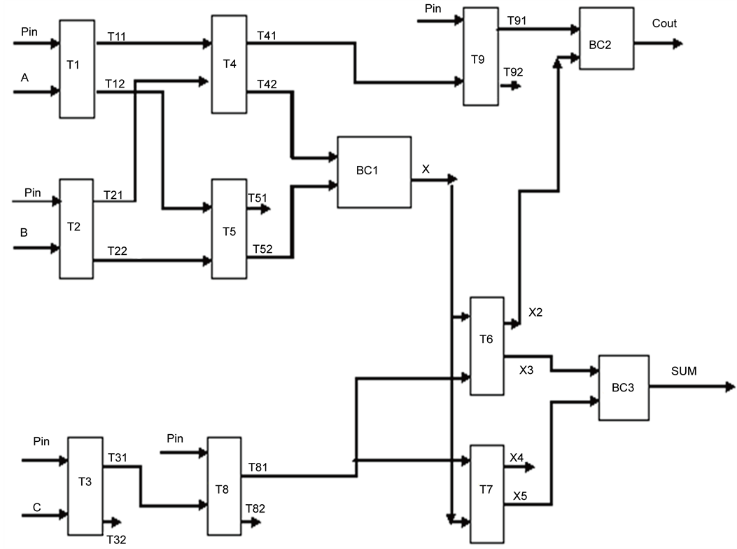
Figure 4. All-optical parallel full adder, A, B, C: Inputs, T1 - T9: TOAD based switches, BC1 - BC3: Beam combiners and Sum, Cout: Outputs.
channel and X3 = 0 from its lower channel. Switch T7 produces output X4 = 0 from its upper channel and X5 = 0 from its lower channel. Now X3 and X5 is combined using BC3 to produce output Sum = 0. X2 and T91 is combined using BC2 to produce Cout = 0.
CASE 2: When A = 0, B = 0 and C = 1. Light emerges out from X5 only i.e., from lower output channel of switch T7. So, T91, X3 and X2 becomes 0. Hence Sum = 1 (X3 + X5) and Cout = 0 (T91 + X2).
CASE 3: When A = 0, B = 1 and C = 0. Light emerges out from X3 only i.e., from lower output channel of switch T6. So, T91, X2 and X5 becomes 0. Hence Sum = 1 (X3 + X5) and Cout = 0 (T91 + X2).
CASE 4: When A = 0, B = 1 and C = 1. Light emerges out from X2 only i.e., from upper output channel of switch T6. So, T91, X3 and X5 becomes 0. Hence Sum = 0 (X3 + X5) and Cout = 1 (T91 + X2).
CASE 5: When A = 1, B = 0 and C = 0. Light emerges out from X3 only i.e., from lower output channel of switch T6. So, T91, X2 and X5 becomes 0. Hence Sum = 1 (X3 + X5) and Cout = 0 (T91 + X2).
CASE 6: When A = 1, B = 0 and C = 1. Light emerges out from X2 only i.e., from upper output channel of switch T6. So, T91, X3 and X5 becomes 0. Hence Sum = 0 (X3 + X5) and Cout = 1 (T91 + X2).
CASE 7: When A = 1, B = 1 and C = 0. Light emerges out from T91 only i.e., from upper output channel of switch T9. So, X2, X3 and X5 becomes 0. Hence Sum = 0 (X3 + X5) and Cout = 1 (T91 + X2).
CASE 8: When A = 1, B = 1 and C = 1. Light emerges out from X5 and T91 i.e., from lower output channel of switch T7 and upper output channel of switch T9 respectively. So, X3 and X2 becomes 0. Hence Sum = 1 (X3 + X5) and Cout = 1 (T91 + X2).
In this way addition of any three bit number can be done with this circuit.
5. Simulated Results
The parameters used in this simulation are taken from the literature survey of different research papers [10] [13] - [15] . The values of different parameters as : unsaturated amplifier gain of the SOA (Gss) = 30 dB, gain recovery time of SOA (τe) = 90 ps, saturation energy of the SOA (Esat) = 700 fJ, eccentricity of the loop (Tasym) = 30 ps, line-width enhancement factor (α) = 6, full width at half maximum of control pulse (σ) = 6 ps, bit period (Tc) = 100 ps, and a control pulse energy (Ecp) = 70 fJ so that the operational conditions are satisfied. The simulated input and output waveforms of half adder are shown in Figure 5 and Figure 6, respectively. The simulated input and output waveforms of full adder are shown in Figure 7 and Figure 8, respectively.

Figure 5. Simulated input waveforms of parallel half adder, where power (Watt) is along the y-axis whereas time (ps) is along the x-axis.

Figure 6. Simulated output waveforms of parallel half adder, where power (Watt) is along the y-axis whereas time (ps) is along the x-axis.

Figure 7. Simulated input waveforms of parallel full adder, where power (Watt) is along the y-axis whereas time (ps) is along the x-axis.
6. Conclusion
In this paper, we have reported parallel all-optical half adder and full adder. Here, in this proposed scheme, the significant advantage is that the proposed circuit can perform addition operations, which are all-optical in nature. This theoretical model has been verified through numerical simulation.

Figure 8. Simulated output waveforms of parallel full adder, where power (Watt) is along the y-axis whereas time (ps) is along the x-axis.
Acknowledgements
The authors are grateful to Technical Education Quality Improvement Programme (TEQIP) phase II by National Project Implementation Unit (Approval No.-CEMK/ TEQIP-lI/R&D/Project/15-16/03) for providing the grant for this work.
Cite this paper
Gayen, D.K. (2016) Optical Arithmetic Operation Using Optical Demultiplexer. Circuits and Systems, 7, 3485-3493. http://dx.doi.org/10.4236/cs.2016.711296
References
- 1. Cotter, D., Manning, R.J., Blow, K.J., Ellis, A.D., Kelly, A.E., Nesset, D., Phillips, I.D., Poustie, A.J. and Rogers, D.C. (1999) Nonlinear Optics for High-Speed Digital Information Processing. Science, 286, 1523-1528.
http://dx.doi.org/10.1126/science.286.5444.1523 - 2. Suzuki, M. and Uenohara, H. (2009) Investigation of All-Optical Error Detection Circuit Using SOA-MZI Based XOR Gates at 10 Gbit/s. Electronics Letters, 45, 224.
http://dx.doi.org/10.1049/el:20093461 - 3. Minh, H.L., Ghassemlooy, Z. and Ng, W.P. (2008) Characterization and Performance Analysis of a TOAD Switch Employing a Dual Control Pulse Scheme in High Speed OTDM Demultiplexer. IEEE Communications Letters, 12, 316-318.
http://dx.doi.org/10.1109/LCOMM.2008.061299 - 4. Li, G. (2009) Recent Advances in Coherent Optical Communication. Advances in Optics and Photonics, 1, 279-307.
http://dx.doi.org/10.1364/AOP.1.000279 - 5. Bhattacharyya, A., Gayen, D.K. and Chattopadhyay, T. (2012) 4-Bit All-Optical Binary to Two’s Complement Converter. Proceedings of International Conference on Communications, Devices and Intelligent Systems, 496-499.
http://dx.doi.org/10.1109/codis.2012.6422247 - 6. Bhattacharyya, A., Gayen, D.K. and Chattopadhyay, T. (2013) Alternative All-Optical Circuit of Binary to BCD Converter Using Terahertz Asymmetric Demultiplexer Based Interferometric Switch. Proceedings of 1st International Conference on Computation and Communication Advancement (IC3A-2013), India, 11-12 January 2013, 1-4.
- 7. Gayen, D.K. and Roy, J.N. (2008) All-Optical Arithmetic Unit with the Help of Terahertz Optical Asymmetric Demultiplexer (TOAD) Based Tree Architecture. Applied Optics, 47, 933-943.
http://dx.doi.org/10.1364/AO.47.000933 - 8. Melo, A.M., Lima, J.L.S., de Oliveira, R.S. and Sombra, A.S.B. (2002) Photonic Time Division Multiplexing (OTDM) Using Ultra-Short Picosecond Pulses in a Terahertz Optical Asymmetric Demultiplexer (TOAD). Optics Communications, 205, 299-312.
http://dx.doi.org/10.1016/S0030-4018(02)01377-9 - 9. Wang, B., Baby, V., Tong, W., Xu, L., Friedman, M., Runser, R., Glesk, I. and Prucnal, P. (2002) A Novel Fast Optical Switch Based on Two Cascaded Terahertz Optical Asymmetric Demultiplexers (TOAD). Optics Express, 10, 15-23.
http://dx.doi.org/10.1364/OE.10.000015 - 10. Zoiros, K.E., Vardakas, J., Houbavlis, T. and Moyssidis, M. (2005) Investigation of SOA- Assisted Sagnac Recirculating Shift Register Switching Characteristics. International Journal for Light and Electron Optics, 116, 527-541.
http://dx.doi.org/10.1364/OE.10.000015 - 11. Sokoloff, J.P., Prucnal, P.R., Glesk, I. and Kane, M. (1993) A Terahertz Optical Asymmetric Demultiplexer (TOAD). IEEE Photonic Technology Letters, 5, 787-789.
http://dx.doi.org/10.1109/68.229807 - 12. Sokoloff, J.P., Glesk, I., Prucnal, P.R. and Boneck, R.K. (1994) Performance of a 50 Gbit/s Optical Time Domain Multiplexed System Using a Terahertz Optical Asymmetric Demul- tiplexer. IEEE Photonics Technology Letters, 6, 98-100.
http://dx.doi.org/10.1109/68.265902 - 13. Eiselt, M., Pieper, W. and Weber, H.G. (1995) SLALOM: Semiconductor Laser Amplifier in a Loop Mirror. Journal of Lightwave Technology, 13, 2099-2112.
http://dx.doi.org/10.1109/50.469721 - 14. Zoiros, K.E., Vardakas, J., Houbavlis, T. and Moyssidis, M. (2005) Investigation of SOA- Assisted Sagnac Recirculating Shift Register Switching Characteristics. International Journal for Light and Electron Optics, 116, 527-541.
http://dx.doi.org/10.1016/j.ijleo.2005.03.005 - 15. Gayen, D.K., Chattopadhyay, T., Das, M.K., Roy, J.N. and Pal, R.K. (2011) All-Optical Binary to Gray Code and Gray to Binary Code Conversion Scheme with the Help of Semiconductor Optical Amplifier-Assisted Sagnac Switch. IET Circuits, Devices & Systems, 5, 123-131.
http://dx.doi.org/10.1049/iet-cds.2010.0069