Circuits and Systems
Vol.06 No.03(2015), Article ID:55133,11 pages
10.4236/cs.2015.63009
Design of a New Serializer and Deserializer Architecture for On-Chip SerDes Transceivers
Nivedita Jaiswal, Radheshyam Gamad
Department of Electronics and Instrumentation Engineering, Shri G. S. Institute of Technology and Science, Indore, India
Email: nivedita.jaiswal27@gmail.com, rsgamad@gmail.com
Copyright © 2015 by authors and Scientific Research Publishing Inc.
This work is licensed under the Creative Commons Attribution International License (CC BY).
http://creativecommons.org/licenses/by/4.0/


Received 13 January 2015; accepted 26 March 2015; published 27 March 2015
ABSTRACT
The increasing trends in SoCs and SiPs technologies demand integration of large numbers of buses and metal tracks for interconnections. On-Chip SerDes Transceiver is a promising solution which can reduce the number of interconnects and offers remarkable benefits in context with power consumption, area congestion and crosstalk. This paper reports a design of a new Serializer and Deserializer architecture for basic functional operations of serialization and deserialization used in On-Chip SerDes Transceiver. This architecture employs a design technique which samples input on both edges of clock. The main advantage of this technique which is input is sampled with lower clock (half the original rate) and is distributed for the same functional throughput, which results in power savings in the clock distribution network. This proposed Serializer and Deserializer architecture is designed using UMC 180 nm CMOS technology and simulation is done using Cadence Spectre simulator with a supply voltage of 1.8 V. The present design is compared with the earlier published similar works and improvements are obtained in terms of power consumption and area as shown in Tables 1-3 respectively. This design also helps the designer for solving crosstalk issues.
Keywords:
SerDes Transceiver, Serializer, Deserializer, SoC, Cadence

1. Introduction
System on Chip (SoC) and System in Package (SiP) technologies provide a path for continued improvement in performance, power, cost and size at the system level without relying upon conventional CMOS scaling alone. These advances allow the number of integrated modules to grow much more rapidly on a single chip [1] or in a single package. These technologies will require a large number of parallel wiring nets and buses for interconnections as well as data communication between these modules. However, in advance technologies, interconnects are not scaling with the same rate as devices. Hence, using parallel metal tracks and buses seems completely inefficient in terms of power, area and crosstalk issues. A promising solution is replacing parallel bus with serial link using a SerDes transceiver [2] - [4] . Serial link based designs have been used for decades in Off-Chip Communications because it offers many advantages over traditional parallel implementations including fewer pins, reduced space requirements, reduced complexity, lower power consumption, smaller connectors, lower electromagnetic interference, and better noise immunity [5] [6] . If the number of channels is reduced where the same channel area is maintained, the significant savings in power dissipation can be achieved. Since the serial link occupies less space due to decreased number of pins, the saved area can be used to isolate the link better from its surrounding components and to integrate more modules [7] . A similar problem exists for On-Chip communication in these new technologies mainly because of power and area overheads.
A number of recent publications have already proposed inspiring solutions for reliable low power on-chip SerDes link with a new self timed signaling technique along differential transmission line or using resistive terminated single ended transmission line [8] [9] . The design presents a variation tolerant driving technique for all digital self timed three levels signaling whereas design uses two level Manchester encoding using resistive termination and power efficient circuitry. Serializer and Deserializer form the basic functional blocks used in On-Chip SerDes Transceiver by all the aforesaid publications [10] [11] . Figure 1 shows the block diagram for SerDes Transceiver presented for On-Chip Networking. The publications have used a double edge triggered flip flop (DETFF) based 8-bit Serializer. Also, a simple shift register based 8-bit Deserializer is used for deserialization [7] - [10] .
This paper reports following new contributions for On-Chip SerDes Transceivers as compared to earlier published work:
・ An improved double edge triggered flip flop (DETFF) based 8-bit Serializer with substantial reduction in power consumption and area requirement.
・ A new Deserializer with same functional throughput but with higher power savings in the clock distribution network along with lower power consumption.
2. Proposed System Architecture
2.1. Design of Serializer
The design of a proposed Serializer is presented in Figure 2 and its block diagram representation is given in Figure 3. Also, Figure 4 depicts block of the Serializer [8] . This work has used double edge triggered flip flop (DETFF) as presented in Figure 5. Each DETFF is composed of two types of flip flops: first is a positive edge triggered flip flop and second is a negative edge triggered flip flop. These flip flops are implemented using clock overlap insensitive clocked CMOS (C2MOS) registers [12] . The combination of these flip flops allows DETFF to sample the input serial data on both clock edges without using additional latch and 2:1 MUX.
Earlier reported work [8] has a Serializer, in Figure 4, where each DETFF uses four blocks: two positive edge triggered flip flops (FF), a negative latch (L) and a 2:1 MUX (M). This means, in the proposed design, authors have reduced the number of blocks. This leads to a substantial reduction in two important parameters namely power consumption and area requirements and a clear comparison is presented in Section 3.1.
Also, in Figure 4, Serializer [8] produces the output serial data sequence in the order D1, D3, D2, D4, D5, D7, D6, D8, D1, D3, ・・・ This may trouble the designer while interpreting the output serialized data. The proposed

Figure 1. Block diagram for SerDes transceiver [8] .

Figure 2. Design of a proposed Serializer.
Serializer design has reordered the parallel data inputs such that the serialized data sequence at the output of Serializer will be obtained as D1, D2, D3, D4, D5, D6, D7, D8, D1, D2... This input reordering is clearly reported in proposed design shown in Figure 3.
2.2. Design of Deserializer
A proposed Deserializer is presented in Figure 6 with its block diagram representation in Figure 7 and the earlier reported simple shift register Deserializer [8] is shown in Figure 8. In this Deserializer, two types of flip flops (FF) are used: a positive edge triggered flip flop and a negative edge triggered flip flop, as presented in Figure 9(a) and Figure 9(b) respectively. These flip flops are implemented using clock overlap insensitive clocked CMOS (C2MOS) registers [12] . The proposed Deserializer is designed such that it samples input on both edges of clock i.e. positive as well as negative edge. The advantage of this technique of input sampling is that a lower clock―half the original rate―is distributed for the same functional throughput, resulting in power savings in the clock distribution network as well as lower power consumption as compared to Deserializer in [8] . A clear comparison in power consumption is presented in Section 3.2.
3. Simulation Results and Discussions
The proposed Serializer and Deserializer architecture are designed using a UMC 180 nm CMOS technology and simulation is done using Cadence Spectre simulator with a supply voltage of 1.8 V.

Figure 3. Block diagram of proposed Serializer.
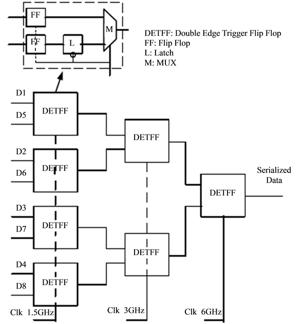
Figure 4. Earlier published Serializer.

Figure 5. Design of a proposed double edge triggered flip flop (DETFF).
3.1. Simulation Results for Serializer
The design serializes 8-bit parallel data at 156.25 MHz into a 1.25 Gbps serial data stream with clocks of frequencies 625 MHz, 312.5 MHz and 156.25 MHz. The simulated result for the signals of the proposed Serializer is presented in Figure 10. Here, parallel data input is “1, 1, 0, 1, 0, 1, 1, 0” and used voltages for each individual parallel data input is as follows: D1 = 1.8 V, D2 = 1.8 V, D3 = 0 V, D4 = 1.8 V, D5 = 0 V, D6 = 1.8 V, D7 = 1.8 V, D8 = 0 V.
From an area perspective, the resources that are used in proposed design is considerably less as mentioned clearly in Figure 3 and Figure 4. In Figure 3, the combination of a positive edge triggered flip flop and a negative edge triggered flip flop allows DETFF to sample the input serial data on both clock edges and obtained same functionality as [8] . Hence, authors have removed the latches and 2:1 MUX’s as compared to the earlier published work by [8] as given in Table 1 and Figure 11.
From power aspect, the elimination of latch and 2:1 MUX leads to a substantial reduction in power as reported by the simulation results obtained for some random parallel data input combinations in Table 2 and
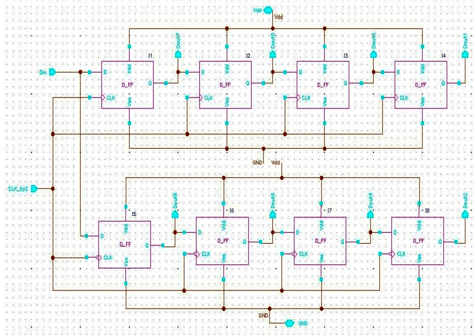
Figure 6. Design of a proposed Deserializer.

Figure 7. Block diagram of proposed Deserializer.

Figure 8. Earlier reported simple shift register based Deserializer [8] .
 (a)
(a) (b)
(b)
Figure 9. (a) Design of a proposed positive edge triggered flip flop (PETFF); (b) Design of a proposed negative edge triggered flip flop (NETFF).
Figure 12. For an appropriate power consumption comparison, both designs (this work and [8] ) are simulated under identical conditions. Both designs serialize 8-bit parallel data at 156.25 MHz into a 1.25 Gbps serial data stream with clocks of frequencies 625 MHz, 312.5 MHz and 156.25 MHz.
3.2. Simulation Results for Deserializer
The design deserializes 1.25 Gbps serial data stream to 8-bit parallel data at 156.25 MHz with clock frequency 625 MHz. The simulated result for the signals of the proposed Deserializer for serial data stream “11010110” is presented in Figure 13.
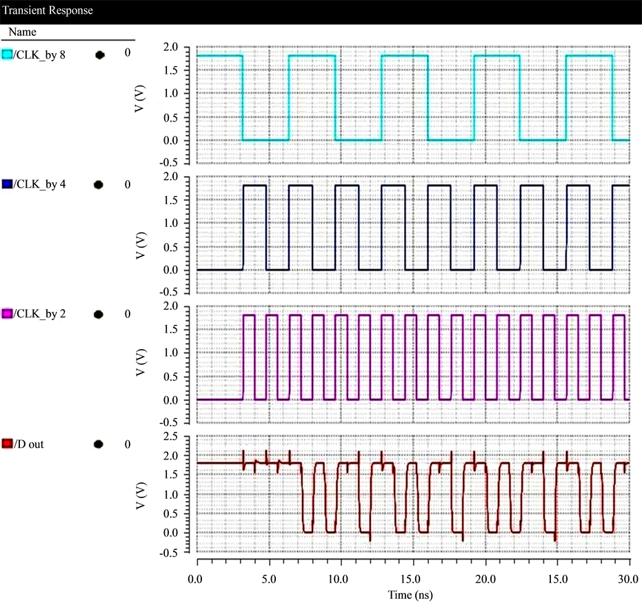
Figure 10. Simulation result of the proposed Serializer for parallel data input “1, 1, 0, 1, 0, 1, 1, 0”.

Table 1. Serializer: Area requirement comparison between earlier work and this work.

Figure 11. Serializer: Area requirement comparison between earlier work and this work.
Table 2. Serializer: Estimated power consumption comparison between earlier work and this work.

Figure 12. Serializer: Estimated power consumption comparison between earlier work and this work.
Although from an area perspective, the resources used in proposed design is almost same as in earlier reported works as shown in Figure 7 and Figure 8. However, a considerable power savings is obtained as reported in Table 3. For an appropriate power consumption comparison, both designs (this work and [8] ) are simulated under identical conditions. Both the designs deserializes 1.25 Gbps serial data stream to 8-bit parallel data at 156.25 MHz with clocks of frequency 625 MHz.

Figure 13. Simulation result of the proposed Deserializer for serial data input “11010110”.
Table 3. Deserializer: Estimated power consumption comparison between earlier work and this work.

Figure 14. Deserializer: Estimated power consumption comparison between earlier work and this work.
From Figure 14, it is observed that power consumption of proposed Deserializer design given in Figure 6 is better than Deserializer [8] .
4. Conclusion
In this paper, an improved architecture for Serializer and Deserializer is proposed which forms the basic functional blocks for On-Chip SerDes transceiver and is proved to consume lower power as compared to similar works done in this particular domain. The proposed Serializer has employed a technique to minimize resources used and hence makes this design area effective as compared to other works. The Serializer also allows ease in decoding serial data obtained after serialization by proper input reordering. A similar improvement is also obtained in the proposed Deserializer as compared to the earlier reported work. This work will be beneficial for the young researchers and designers. Finally, authors have concluded the work and the improvements in the results are observed as reported in this paper.
Acknowledgements
This work has been carried out in SMDP VLSI Laboratory of the Electronics and Instrumentation Engineering Department of Shri G. S. Institute of Technology and Science, Indore, India. This SMDP VLSI project is guided by Ministry of Information and Communication Technology, Government of India. Authors are thankful to the ministry for facilities provided under this project.
References
- Alser, M.H. and Assaad, M.M. (2011) Design and Modeling of Low-Power Clockless Serial Link for Data Communication Systems. National Postgraduate Conference, Kuala Lumpur, 19-20 September 2011, 1-5. http://dx.doi.org/10.1109/NatPC.2011.6136441
- Geurts, T., Rens, W., Crols, J., Kashiwakura, S. and Segawa, Y. (2004) A 2.5 Gbps - 3.125 Gbps Multi-Core Serial- Link Transceiver in 0.13 μm CMOS. Proceeding of the 30th European Solid-State Circuits Conference, 21-23 September 2004, 487-490. http://dx.doi.org/10.1109/ESSCIR.2004.1356725
- Park, J.Y., Kang, J., Park, S. and Flynn, M.P. (2009) A 9 Gbit/s Serial Transceiver for On-Chip Global Signaling over Lossy Transmission Lines. IEEE Transactions on Circuits and Systems (TCAS), 56, 1807-1817. http://dx.doi.org/10.1109/TCSI.2009.2027634
- Philpott, R.A., Humble, J.S., Kertis, R.A., Fritz, K.E., Gilbert, B.K. and Daniel, E.S. (2008) A 20Gb/s SerDes Transmitter with Adjustable Source Impedance and 4-Tap Feed-Forward Equalization in 65 nm Bulk CMOS. IEEE Custom Integrated Circuits Conference (CICC), San Jose, 21-24 September 2008, 623-626.
- Chen, D.Y. (2007) SerDes Transceivers for High Speed Serial Communications. Department of Electronics, Carleton University, Ottawa.
- Bhatti, R.Z., Denneau, M. and Draper, J. (2006) 2 Gbps SerDes Design Based on IBM Cu-11 (130 nm) Standard Cell Technology. 16th ACM Great Lakes Symposium on VLSI, 198-203.
- Ghoneima, M., Ismail, Y., Khellah, M., Tschanz, J. and De, V. (2009) Serial Link Bus: A Low-Power On-Chip Bus Architecture. IEEE Transactions on Circuits and Systems I (TCAS), 2020-2032.
- Safwat, S., Hussein, E.E., Ghoneima, M. and Ismail, Y. (2011) A 12 Gbps All Digital Low Power SerDes Transceiver for On-Chip Networking. 2011 IEEE International Symposium on Circuits and Systems (ISCAS), Rio de Janeiro, 15-18 May 2011, 1419-1422. http://dx.doi.org/10.1109/ISCAS.2011.5937839
- Hussein, E.E., Safwat, S., Ghoneima, M. and Ismail, Y. (2012) A 16 Gbps Low Power Self Timed SerDes Transceiver for Multi-Core Communication. 2012 IEEE International Symposium on Circuits and Systems (ISCAS), Seoul, 20-23 May 2012, 1660-1663. http://dx.doi.org/10.1109/ISCAS.2012.6271576
- Tadros, R.N., Elsayed, A.H., Ghoneima, M. and Ismail, Y. (2014) A Variation Tolerant Driving Techniques for All- Digital Self-Timed 3-Level Signaling High-Speed SerDes Transceiver for On-Chip Networks. 2014 IEEE International Symposium on Circuits and Systems (ISCAS), Melbourne, 1-5 June 2014, 1520-1523. http://dx.doi.org/10.1109/ISCAS.2014.6865436
- Elsayed, A.H., Tadros, R.N., Ghoneima, M. and Ismail, Y. (2014) Low Power All-Digital Manchester Encoding Based High-Speed SerDes Transceiver for On-Chip Networks. 2014 IEEE International Symposium on Circuits and Systems (ISCAS), Melbourne, 1-5 June 2014, 2752-2755. http://dx.doi.org/10.1109/ISCAS.2014.6865743
- Suzuki, Y., Odagawa, K. and Abe, T. (1973) Clocked CMOS Calculator Circuitry. IEEE Journal of Solid State Circuits, 8, 462-469. http://dx.doi.org/10.1109/JSSC.1973.1050440