Circuits and Systems
Vol. 3 No. 3 (2012) , Article ID: 20202 , 8 pages DOI:10.4236/cs.2012.33032
Power Conversion Enhancement of CdS/CdTe Solar Cell Interconnected with Tunnel Diode
Communications and Electronics Department, Faculty of Engineering, Philadelphia University, Amman, Jordan
Email: {wagahfaljubori, oamr1462004}@yahoo.com, munther_baker44@yahoo.co.uk
Received March 20, 2012; revised April 20, 2012; accepted April 27, 2012
Keywords: CdS/CdTe; Solar Cells; Energy Conversion; Efficiency
ABSTRACT
One of the most promising solar cell devices is cadmium telluride (CdTe) based. These cells however, have their own problems of stability and degradation in efficiency. Measurements show that CdS/CdTe solar cell has high series resistance which degrades the performance of solar cell energy conversion. Both active layers (CdS and CdTe) had been fabricated by thermal evaporation and tested individually. It was found that CdS window layer of 300 nm have the lowest series resistance with maximum light absorption. While 5 - 7 µm CdTe absorber layer absorbed more than 90% of the incident light with minimum series resistance. A complete CdS/CdTe solar cell was fabricated and tested. It was found that deposited cell without heat treatment shows that the short circuit current increment decreases as the light intensity increases. This type of deposited cell has low conversion efficiency. The energy conversion efficiency was improved by heat treatment, depositing heavily doped layer at the back of the cell and minimizing the contact resistivity by depositing material with resistivity less than 1 mΩ·cm2. All these modifications were not enough because the back contact is non-ohmic. Tunnel diode of CdTe (p++)/CdS (n++) was deposited in the back of the cell. The energy conversion efficiency was improved by more than 7%.
1. Introduction
Silicon-based solar cells are currently the most successful commercial photovoltaic product. The PV market, dominated by crystalline silicon, has grown on average more than twenty percent per year but faces the problem of profitability as it must compete with traditional sources and methods of energy conversion. To become competitive, PV materials are needed as they are much less expensive than single crystal silicon and are compatible with large scale manufacturing. Thin film materials and manufacturing processes are an obvious choice for lowering the cost. Thin film solar cells based on polycrystalline Cadmium Telluride (CdTe) reached record efficiencies of 16.5% [1] for laboratory scale device and of 10.9% for terrestrial module [2]. Since the record efficiency of such type solar cells is considerably lower than the theoretical limit of 28% - 30% [3], the performance of the modules can be improved, through new advances in fundamental material science and engineering, and device processing. CdTe is one of the most suitable materials for photovoltaic applications. CdTe has a direct band gap material (Eg ≈ 1.5 eV at room temperature) with a high absorption coefficient (above 105 cm–1 at the wavelength of 700 nm). Few microns thick layer of CdTe absorbs more than 90% of the incident light with the photon energy higher than the band gap. The maximum theoretical efficiency corresponding to such band gap is about 27%. The small thickness required for an absorbing layer makes the cost of material for the solar cells relatively low. To date, CdTe has been deposited successfully by a variety of techniques [4].
CaCadmium sulfide (CdS) belonging to the II-VI group is one of the promising materials for optoelectronic devices. CdS has been the subject of intensive research because of its intermediate band gap (Eg ≈ 2.42 eV) making the material suitable as window material for a heterojunction solar cell [5], high absorption coefficient, reasonable conversion efficiency, stability and low cost [6]. Knowledge of the optical properties of CdS films is very important in the field of optoelectronic devices like photo-detectors and solar cells. A broad variety of deposition techniques can be used to fabricate CdS films with desirable optical properties [7]. Although CdTe can be doped both p-type and n-type CdTe: homojunction cells have not shown very high efficiency. Due to high absorption coefficient and small diffusion length, the junction must be formed close to the surface, which reduces the carrier lifetime through surface recombination. The In-doped CdTe (p) thin film is of high bulk resistivity which largely affects its photovoltaic properties particularly the short circuit current [8]. It was noted that, the deteriorative effect of the high bulk resistivity increases by increasing the light intensity, which in turn limits the benefit of using light concentrators that improve the short circuit current.
Heterojunctions which consist of CdTe as one of the junction sides had been under investigation for many years [9]. The electrical properties of post-deposition annealed and as-deposited In-doped CdTe thin films were studied in details [10]. It was observed that the CdTe film was of modified Poole-Frenkel conduction mechanism and the resistivity of the film could be lowered by more than one order of magnitude due to indium doping. Also, considerable amount of work had been paid to develop the CdS/CdTe solar cells over the last twenty years [11]. Also the electrical, photoelectrical, and structural properties of CdS/CdTe heterostruture were studied [12]. Deposition of thin polycrystalline CdTe layers on the top of the CdS layer for solar cells has been successfully performed by using various methods. Considerably higher efficiencies were obtained by using n-CdS/p-CdTe heterojunctions. The CdS layer serves as a window layer and helps to reduce the interface recombination. Without special doping the CdS film has significantly higher carrier concentration (≈1016 - 1017 cm–3) than the CdTe adjacent to the interface (≈1014 - 1015 cm–3). As a result the built-in potential is applied mostly to the CdTe absorber layer, providing effective separation of the photo generated carriers. High efficiency solar cells of efficiencies up to 12.5% were developed with a CdTe low temperature (<450˚C) process [13]. Efficient solar cell performance requires minimizing the forward recombination current and maximizing the light generated current. Collection losses can be minimized in thin film of high absorption and short diffusion length. Voltage dependent photocurrent collection losses in CdTe films were observed [14]. The voltage dependence of photocurrent of CdTe/CdS solar cells was characterized by separating the forward current from the photocurrent. Recently, preparation and performance of CdS/CdTe tandem solar cells is introduced [15,16]. Thinner layers at the top and thicker ones at the bottom managed to increase the open circuit voltage and improve the spectral response.
2. Laboratory Preparations and Solar Cell Structure
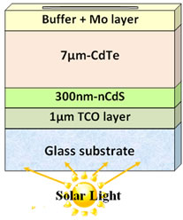
Cadmium Sulphide/Cadmium telluride (CdS/CdTe) solar cell is composed of four main layers deposited on a glass substrate. A transparent conducting oxide deposited directly on top of the glass to form the front contact. The second layer is the window layer, which is usually n-type semiconductor. CdS, with band gap of 2.4 eV at room temperature, is the most suitable material for CdTe-based solar cells. The work of [17-19] showed that without special doping, the CdS films have significantly higher carrier concentration than the CdTe. The third layer is the absorber layer of CdTe, which is usually from 5 - 10 µm thick film. The deposition parameters, optical and electrical properties of active layers will be discussed deeply later. Finally, the fourth step in the solar cell fabrication is the application of the back electrical contact to the CdTe layer. 2 µm Aluminum is used as metal back contact. It was recognized that this step is critical for CdS/ CdTe solar cell performance due to low stability and resulted in a high contact resistance. In order to minimize this resistance (ρC < 1 mΩ·cm) tunnel diode is proposed to be connected in series with the solar cell [20]. These problems will be the main issues in this work and they will be addressed later.
Fabrication of CdS films of thickness up to 800 nm was carried out on a glass substrate using Balzer vacuum thermal evaporation system. The substrate temperature, vacuum pressure, deposition rate, film thickness and annealing temperature have been measured by the system. CdS film was evaporated at optimum evaporation parameters [18], under 10–6 mbar vacuum. The substrate temperature was 300˚C and the deposition rate is 2˚ A/sec. Thickness of the layer and annealing temperature are varied to obtain maximum grain size at minimum thickness with very low resistivity. Few samples of CdTe thin film were prepared by thermal evaporation and deposited on glass substrate to be examined individually. A comprehensive study of CdTe layer in CdS/CdTe solar cell had been conducted [21], and the main parameters of CdTe material that affect the module efficiency had been discussed. Among these parameters are the lifetime, diffusion length, drift length of minority carriers and thickness of CdTe absorber layer. In this research; it is found that 7 µm of CdTe thickness deposited with 8˚ A/sec. rate of deposition on substrate with 100˚C temperature is optimum for maximum absorption of radiation and produces large enough grain size [10]. The annealing temperature is varied for optimum optical and electrical properties of the film.
3. Optical and Electrical Properties of the Solar Cell Layers
Transmission and absorption coefficient spectrum have been carried out for each individual layer at different annealing temperature. Figures 1 and 2 shows the transmission and absorption coefficients of CdS and CdTe layers respectively. CdS film exhibited high degree of transmittance in the infrared region and showed sharp falling of the absorption edge towards lower wavelength. The absorption edge is lowered as the annealing tem-
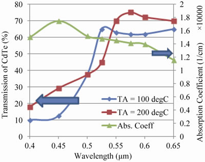
Figure 1. Transmittance and absorption coefficients of CdS layer at different annealing temperatures.
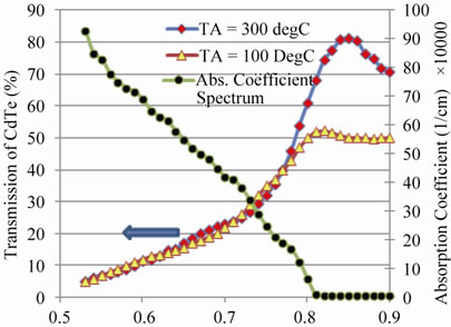
Figure 2. Transmittance and absorption coefficients of CdTe layer at different annealing temperatures.
perature of the film increased. It was found that small changes in the thickness of CdS had a greater influence on transmission. It must, however, be emphasized that more reduction of CdS will increase the resistivity of the layer which will deteriorate the electrical properties of the layer. Thicker CdTe layer is used in order that all light is absorbed in this layer. CdTe film exhibits transmittance at short wavelength (λ ≈ 500 nm). The transmittance becomes more pronounced at wavelength higher than 800 nm. The absorption edge shifted toward lower wavelength at high annealing temperature (250˚C).
Figures 3 and 4 show that the variation of resistivity and photo generated current of CdS and CdTe layers with wavelength at different annealing temperatures. It is clear that CdS sample annealed at 250˚C gave minimum resistivity and of course maximum photo generated current. This is because that the absorption coefficient for this sample is very high which is inversely proportional to resistivity. The material becomes more n-type due to excessive Cadmium under layer and enhanced diffusion at grain boundaries or impurities incorporated in the deposit [7].
4. The Effect of Series Resistance
Figure 5(a) represents a schematic representation of the CdS/CdTe solar cell heterostructure. The layers succession and thicknesses are the one used in the present work. An electronic solar cell model can be considered, as shown in Figure 5(b), taking into account the effect of the series resistance (Rs) and shunt resistance (Rsh). The solar cell current source generates a light current (IPH) which is directly proportional to the solar illumination. The two resistors (Rsh) and (Rs) represent the losses incurred in the solar cell. The series resistor (Rs) caused by the ohmic losses in the surface of the solar cell. The par-
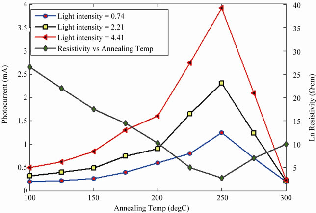
Figure 3. Variation of resistivity and photo generated current with annealing temperature for CdS layer.
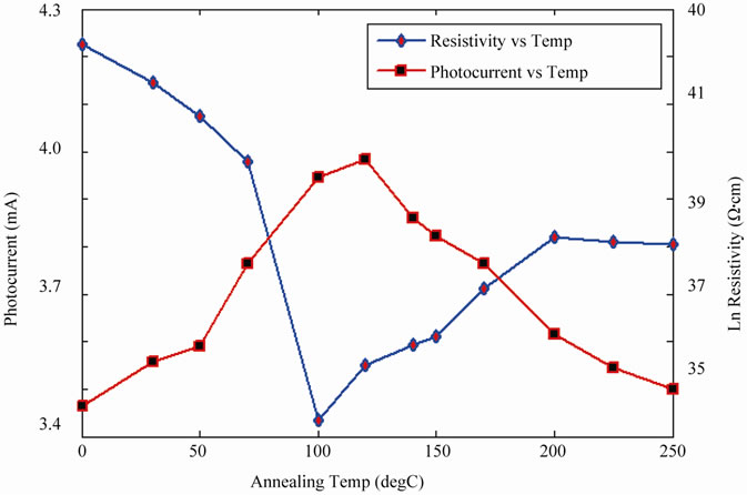
Figure 4. Variation of resistivity and photo generated current with annealing temperature for CdTe layer.
 (a)
(a)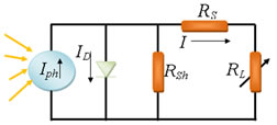 (b)
(b)
Figure 5. (a) Schematic representation of the CdS/CdTe solar cell heterostructure; (b) Electronic solar cell model.
allel shunt resistor (Rsh) denotes the losses due to leakage current in the solar cell.
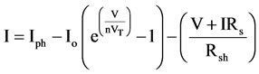
Taking into account the effect of the series resistance (Rs) and shunt resistance (Rsh), the current supplied to the load (I) can be expressed as:
 (1)
(1)
where Iph is the photo generated current, Io is the saturation current, V is the applied voltage, n is the identity factor and VT is thermal voltage which is equal to 26 mV at room temperature. The saturation current is measured to be equal to 2 µA. The series resistance is determined as [22].
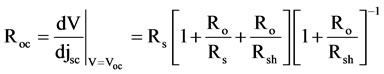 (2)
(2)
where Roc is the open circuit series resistance and Ro = [nkT/q·Jsc]. Usually for CdTe based cells, Jsc ≈ 20 mA/cm2 and n = 2 [8], hence Ro ≈ 2.5 Ω at room temperature. Rsh is usually of order of few several hundred Ohms which means  leads to an approximate relation: Rs ≈ Roc – Ro. Hence the calculated range of series resistance is 5 - 10 Ω. I-V characteristics of CdS/CdTe show that the device has high series resistance [8]. The real value of measured series resistance is higher than the calculated one due to the parasitic resistance connected in series to the main cell. Figure 6 shows the variation of the short circuit current with the light intensity measured practically. It can be seen that the short circuit current

Figure 6. Variation of short circuit current density with light intensity.
varies rapidly at low intensity (<5 mW) while it saturates at high intensity. It can be suggested that this degradation in the cell performance at high light intensities is due to the high series resistance.
The solar cell model given by Equation (1) is simulated using MATLAB. The photo generated current density is measured using the following equation [8]:
 (3)
(3)
q is the electron charge, F is the number of incident photons with energies greater than the band energy in [cm–2·s–1], R is the reflection coefficient, α is the absorption coefficient (cm–1), d is the cell thickness which is nearly equal to CdTe, and η is the collection efficiency which varies from 0 - 1. The limits of integration are from 0.48 - 0.87 µm; out of this range the absorption process can be ignored. The reflection coefficient varies from 0.7 - 0.9 for the wavelength mentioned above. The absorption coefficient can be deduced from Figure 2, which is approximately equals to 1.3 × 107 cm–1. Figure 7 shows that the simulation result and practical measurements of short circuit current versus photo generated current at different values of series resistance with shunt resistance is 10 KΩ. The results given in Figure 8 were calculated at high light intensity (high photo generated currents) which in turn means high short circuit current.
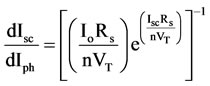
Mathematical manipulation of Equation (1) at short circuit current condition when the voltage across the load resistance becomes zero yields:
 (4)
(4)
It can be seen that the slope varies inversely with Rs that means the variation of Isc will be less as the Iph increases due to the high effect of Rs. That is evidently shown in Figure 7, when Rs becomes zero the slope  will be equal to one; that means the change in the short circuit current equals to the change in photo generated current. The deterioration effect of the high series resistance increases by increasing the light intensity. This will limit the benefit of using light concentrators and improve the short circuit current. Many researches have been carried out to reduce the effect of series resistance. Post-deposition heat treatment with CdCl2 to activate CdTe (p) would probably reduce the series resistance and possibly improve ohmic contact performance [23]. Another improvement of CdS/CdTe solar cell can be achieved in the fill-factor. The improvement is achieved by depositing a thin heavily doped p-type semiconductor with a high work function at the back of CdTe layer [24]. Small valence band (<0.2 eV) would be formed between CdTe layer and metal leads to a low or zero potential barrier at the interface and hence an easy hole transport between the two layers. Figure 8 shows the improvement in quantum efficiency at different annealing temperatures (curves 1 & 2) and depositing thin layer of Te (curve 3) compared with theoretically calculated (curve 4).
More improvements have been made by varying the thickness of CdTe layer. Considering the information of the drift and diffusion components of the photocurrent will lead to the calculation of the short circuit current. Calculation of short circuit current gives an expression of quantum efficiency spectra [21]. In order to reach the total change collection at CdTe layer, the thickness should
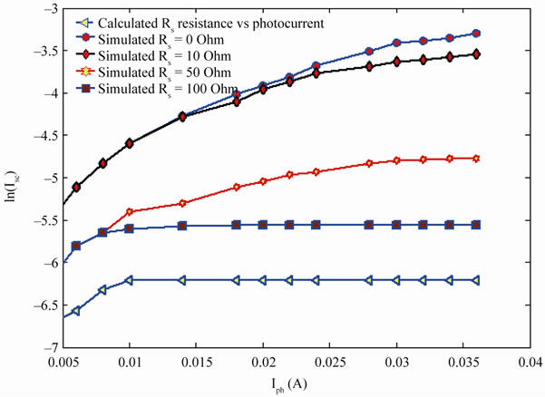
Figure 7. Simulated and calculated short circuit current versus photo current at different values of series resistance.
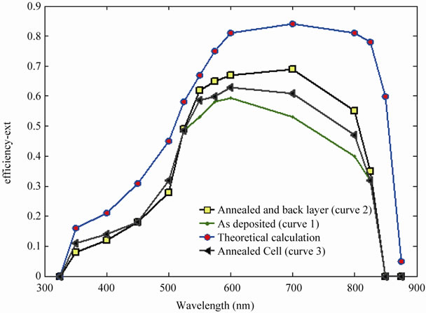
Figure 8. Improvement the quantum efficiency of the solar cell: (1) As deposited; (2) Annealed; (3) With deposited layer and (4) Theoretical calculated.
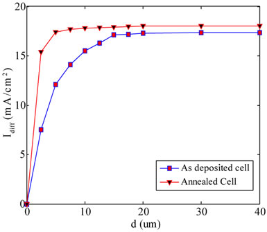
Figure 9. Variation of quantum efficiency of CdS/CdTe solar cell for different values of CdTe thickness: (1) As deposited cell; (2) Annealed cell.
be 50 µm or more [25]. Layer thickness can be reduced by shortening electron life time and hence electron diffusion length. Figure 9 shows the variation of quantum efficiency of the annealed CdS/CdTe cell for different values of CdTe layer thickness. More than 83% efficiency has been detected at 10 µm thickness with the highest efficiency in the gradual transition between 500 nm and 800 nm (the characteristics of the intermixing between CdTe and CdS layer). High quantum efficiency at the thinner CdTe layer achieved due to the increasing of absorption coefficient. As soon as the photon energy exceeds the band gap of CdTe, the absorption coefficient becomes higher than 104 cm–1 i.e. the effective penetration depth becomes less than 10–4 cm (1 nm). This is the reason behind the choice of a few microns (5 - 10 µm) thickness of the CdTe layers. It is evident that the resistance between the CdTe layer and metal back contact is non-ohmic [10]. Actually, there are two diode circuits; the first one is the CdS/CdTe junction (main diode) and the second one is the back contact Schottky diode, which they are connected opposite to each other. Thus, distribution of the applied voltage between the two diodes changes in favor of Schottky diode when applying forward bias voltage to the cell. There is a decrease in the resistance of the main diode and increase that of the Schottky diode.
The above discussions means that the value of the series resistance depends on the voltage applied and current flowing through the cell. According to Schottky theory, the formation of an ohmic contact between a p-type semiconductor and metal results in a high contact resistance due to high potential barrier. Creating a highly doped p++ layer at the surface of CdTe can reduce the effects of the back contact potential barrier. Thinner potential barrier (lower the depletion layer width) produces tunneling or thermally assisted tunneling carrier transport mechanism. The individual sub cell of multi-junction solar cell is interconnected via interband tunnel diode [20]. They feature both low electrical resistivity and high optical transmittance. Reliable simulations of the tunnel diode behavior are still a challenge for solar cell application. Theoretical and experimental measurements of current voltage (I-V) characteristics of tunnel diodes and solar cells had been studied [26]. It is concluded that as the short circuit current of the cell is lower than the maximum tunneling current, the tunnel diode is operated in the state with lower voltage drop. Hence, the tunnel diode acts like an almost ohmic resistor and will not reduce the maximum power output of the solar cell. If the short circuit current of the cell exceeds the maximum tunneling current, the tunnel diode works in the region where thermal current dominated and high voltage drop occurs over the tunnel diode. I-V curve of the solar cell will be sheared to lower voltages. The test structure consisting of CdS/CdTe solar cell with underlying tunnel diode can be regarded as a series of two diodes connected back-to-back as shown in the left side of Figure 10. The tunnel diode is formed by high doping thin layer of CdTe to produce p++ (5 × 10¹⁹/cm3), then depositing another highly doped CdS to produce n++ (3 × 10¹⁹/cm3). The tunnel diode is designed to be able to have a peak current may exceeds values of 50 mA/cm2. Measured IV characteristics of a CdS/CdTe solar cell with CdTe (p++) CdS (n++) tunnel diode is shown in the right side of Figure 10.
Circled line marks the measurement at low light concentration (<50 mW/cm2), causing the short circuit current of the cell to be lower than the maximum tunneling current. The short circuit current is increased as long as the photo generated current is increased. Consequently the maximum power output with the solar cell is increased. Dashed line in Figure 10 marks the measurements at higher light concentration (>50 mW/cm2) causing the short circuit current to exceed the maximum tunneling current. When critical illumination is reached, the cell current exceeds the tunneling current of the tunnel diode and voltage dip appears in the I-V characteristics.
5. Conclusion
CdTe based solar cell is a leading technology in thin film energy conversion efficiency. Their energy conversion efficiency is degraded by the high series resistance of the cell. The resistance is a combination of contact resis-
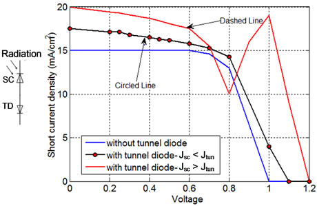
Figure 10. I-V characteristics of a CdS/CdTe solar cell. (a) Without tunnel diode; (b) With tunnel diode and Jsc > Jtun; (c) With tunnel diode and Jsc < Jtun.
tances, semiconductor resistance and non-ohmic ones of the back contact. The contact resistance and semiconductor resistances can be modified by annealing, fabrication parameter and using materials of low resistivity at the contacts. The non-ohmic contact can be modified by connecting tunnel diode at the back of the cell. The only limitation to this approach is that the short circuit current of the cell should not exceed the maximum tunneling current of the tunnel diode. More research and study about this point is needed. AC measurements in wide range of frequencies should be carried out to measure impedances of both diodes and then more adequate physical model can be suggested.
REFERENCES
- X. Wu, J. C. Keane, R. G. Dhere, C. DeHart, A. Duda, T. A. Gessert, S. Asher, D. H. Levi and Sheldon, “16.5% Efficient CdS/CdTe Polycrystalline Thin-Film Solar Cell,” Proceedings of the 17th E-PVSEC, München, October 2001, pp. 995-1000.
- D. Cunningham, K. Davies, L. Grammond, E. Mopas, M. O’Connor, M. Rubcich, M. Sadeghi, D. Skinner and T. Trumbly, “Large Area Apollo Module Performance and Reliability,” Proceedings of the 28th IEEE Photovoltaic Specialists Conference, Fairfield, 2000, pp. 13-18. doi:10.1109/PVSC.2000.915743
- S. Sze, “Physics of semiconductor Devices,” 2nd Edition, Wiley, New York, 1981.
- R. Birkmire, “CdTe1–xSx Absorber Layers for Thin-Film CdTe/CdS Solar Cells,” 26th IEEE Photovoltaic’s Specialists Conference (PVSC), Anaheim, Vol. 295, 1997, pp. 307- 312.
- M. V. Garcia-Cuenc, J. L. Morenza, E. Bertran and A. Lousa, “Electrical Conduction in Polycrystalline CdS Films: Comparison of Theory and Experiment,” Journal of Physics D: Applied Physics, Vol. 20, No. 7, 1987, pp. 958-962. doi:10.1088/0022-3727/20/7/020
- A. Sanchez, P. J. Sebastian and O. Gomez-Daza, “LowResistivity CdS Thin Films Formed by a New Chemical Vapor Transport Method,” Semiconductor Science and Technology, Vol. 10, No. 1, 1995, pp. 87-90. doi:10.1088/0268-1242/10/1/014
- W. F. Mohammed, “The Effect of Temperatures and Doped Level on CdS Thin Films,” Engineering & Technology Journal, Vol. 14, No. 7, 1995, p. 34.
- W. F. Mohammed and M. A. Shehathah, “Effect of Series Resistance on Photovoltaic Properties of In-Doped CdTe (p) Thin Film Homojunction Structure,” Renewable Energy, Vol. 21, No. 3, 2000, pp. 141-152. doi:10.1016/S0960-1481(00)00008-2
- F. Zhou, X. C. Wang, H. C. Wu and C. Z. Zhao, “Achievements and Challenges of CdS/CdTe Solar Cells,” International Journal of Photo Energy, Vol. 2011, 2011, pp. 1-8.
- W. F. Mohammed and M. A. Shehathah, “The Electrical Properties of Post-Deposition Annealed and As-Deposited In-Doped CdTe Thin Films,” Renewable Energy, Vol. 26, 2002, pp. 285-249. doi:10.1016/S0960-1481(00)00195-6
- M. M. Al-Jassim, R. G. Dhere, K. M. Jons, F. S. Hasoon and Sheldon, “The Morphology, Microstructure, and Luminescent Properties of CdS/CdTe Films,” 2nd World Conference and Exhibition on Photovoltaic Solar Energy Conversion, Vienna, 6-10 July 1998.
- D. H. Levi, L. M. Woods, D. S. Albin and T. A. Gessert, “The Influence of Grain Boundary Diffusion on the Electro-Optical Properties of CdTe/CdS Solar Cells,” 2nd World Conference and Exhibition on Photovoltaic Solar Energy Conversion, Vienna, 6-10 July 1998.
- G. Khrypunov, A. Romeo, F. Kurdesau, D. L. Batnzer, H. Zogg and D. L. Tiwari, “Recent Development in Evaporated CdTe Solar Cells,” Solar Energy Material and Solar Cells, Vol. 90, No. 6, 2006, p. 664. doi:10.1016/j.solmat.2005.04.003
- S. Hegedus, D. Desai and C. Thompson, “Voltage Dependent Photocurrent Collection in CdTe/CdS Solar Cells,” Progress Photovoltaic: Research and Applications, Vol. 15, No. 7, 2007, p. 587. doi:10.1002/pip.767
- Y. J. Li, et al., “Preparation and Performance of CdS/ CdTe Tandem Solar Cells,” Chinese Journal of Semiconductors, Vol. 5, 2007, pp. 722-725.
- X. Mathew, J. Drayton, V. Parikh, N. R. Mathews, X. X. Liu and A. D. Compaan, “Development of a Semitransparent CdMgTe/CdS Top Cell for Applications in Tandem Solar Cells,” Semiconductor Science Technology, Vol. 24, No. 1, 2009, Article ID: 015012. doi:10.1088/0268-1242/24/1/015012
- W. F. Mohammed and A. Nori, “The Photo-Electric and Thermal Properties of Vacuum Deposited CdS Thin Films,” Renewable Energy Journal, Vol. 14, No. 1-4, 1998, pp. 129-134. doi:10.1016/S0960-1481(98)00058-5
- W. F. Mohammed and A. Nori, “The Effect of Deposition Parameters on Hall Mobility and Carrier Concentration of CdS Thin Films,” Abhath Al-Yarmook Journal, Vol. 11, No. 1B, 2002, pp. 402-412.
- H. A. Ahmed and L. S. Ali, “Characterization of In-Doped CdTe Thin Film,” Muutah Journal for Research and Studies, Vol. 11, No. 5, 1996, pp. 207-218.
- W. Guter, F. Dimroth, M. Meusel and A. W. Bett, “Tunnel Diodes for III-V Multi-Junction Solar Cells,” 20th European Photovoltaic Solar Energy Conference, Barcelona, June 2005, pp. 515-518.
- L. Kosyachenko, “Efficiency of Thin-Film CdS/CdTe Solar Cells,” In: R. D. Rugescu, Ed., Solar Energy, 2010, pp. 105-130. doi:10.5772/8065
- M. Wolf and H. Rauschenbusch, “Series Resistance Effects on Solar Cell Measurements,” Advanced Energy Conversion, Vol. 3, 1963, pp. 455-479. doi:10.1016/0365-1789(63)90063-8
- A. W. Brinkman and S. M. Al-Amri, “Thin Film CdTe Based Solar Cell,” Proceedings of the 6th Arab International Solar Energy Conference, Muscat, 1998.
- J. Sites and J. Pan, “Strategies to Increase CdTe SolarCell Voltage,” Thin Solid Films, Vol. 515, No. 15, 2007, pp. 6099-6102. doi:10.1016/j.tsf.2006.12.147
- N. Amin, K. Sopian and M. Konagai, “Numerical Modeling of CdS/CdTe and CdS/CdTe/ZnTe Solar Cells as a Function of CdTe Thickness,” Solar Energy Materials and Solar Cells, Vol. 91, No. 13, 2007, pp. 1202-1208. doi:10.1016/j.solmat.2007.04.006
- W. Guter and A. W. Bett, “I-V Characterization of Tunnel Diodes and Multijunction Solar Cells,” IEEE Transactions on Electron Devices, Vol. 53, No. 9, 2006, pp. 2216-2222. doi:10.1109/TED.2006.881051