Circuits and Systems
Vol. 3 No. 2 (2012) , Article ID: 18537 , 8 pages DOI:10.4236/cs.2012.32020
A Parallel Circuit Simulator for Iterative Power Grids Optimization System
1Department of VLSI System Design, Ritsumeikan University, Kusatsu, Japan
2Department of Information Engineering, Meijo University, Nagoya, Japan
Email: mfukui@se.ritsumei.ac.jp
Received January 9, 2012; revised February 20, 2012; accepted February 28, 2012
Keywords: Dedicated Hardware Accelerator; Power Grids Optimization; Parallel Circuit Simulator
ABSTRACT
This paper discusses a high efficient parallel circuit simulator for iterative power grid optimization. The simulator is implemented by FPGA. We focus particularly on the following points: 1) Selection of the analysis method for power grid optimization, the proposed simulator introduces hardware-oriented fixed point arithmetic instead of floating point arithmetic. It accomplishes the high accuracy by selecting appropriate time step of the simulation; 2) The simulator achieves high speed simulation by developing dedicated hardware and adopting parallel processing. Experiments prove that the proposed simulator using 80 MHz FPGA and eight parallel processing achieves 35 times faster simulation than software processing with 2.8 GHz CPU while maintaining almost same accuracy in comparison with SPICE simulation.
1. Introduction
With the deep submicron technologies, it has become possible to mount a large and high performance system on one VLSI chip. However, the power supply voltage is lowering along with shrinking of the device size. On the other hand, the power consumption is increasing because the number of transistors and the clock frequency increase. Therefore, IR-drop and electro-migration (EM) in the power grids make functions and devices unreliable. It becomes more serious problem than ever. The power grid optimization has become very important for ensuring the reliability, correctness and stability of the design. In recent years, many prior researches [1-6] have been proposed to solve the problem. A heavy simulation time is required to analyze the problem of heat and electromagnetic field [3]. Moreover, a high speed and high accurate circuits simulator is required for iterative optimization which includes execution of the simulation many times for its evaluation.
Thus, several hardware accelerator approaches have been reported [7-12]. Lee et al. achieved 25 times high speed processing in the timing verification using multi CPU [7]. Nakasato et al. demonstrated particle simulation by floating point arithmetic on an FPGA [8]. Watanabe et al. introduced parallel-distributed time-domain circuit simulation of power distribution networks by multiple PC [9]. However, no research of hardware accelerator to optimize power grids of VLSI has been reported.
This paper aims at estimating the performance improvement by hardware implementation of the circuit simulation in the power supply wiring. We have analyzed accuracy, speed, and hardware resources to implement typical numerical analysis algorithms of circuit simulation, in cases of floating point and fixed point variables, software and hardware. Moreover, we propose an efficient hardware circuit simulator for power grid optimization. It achieves high speed simulation by adopting pipeline and parallel processing. The proposed simulator introduces hardware-oriented fixed point arithmetic instead of floating point arithmetic. The hardware-oriented fixed point arithmetic realizes the high area-efficiency by reducing hardware resources, and it also accomplishes the high accuracy by controlling intervals of simulation.
2. Power Grid Optimization System
2.1. Power Grid Optimization Algorithm
The power grid consists of two vertical and horizontal layers. Those are interconnected by contacts at the intersection. The equivalent circuit model for proposed power grid optimization system is shown in Figure 1.
Decoupling capacitors are inserted to decrease dynamic IR-drop and inductor noise to the power grid. At each grid area, four edges of resistances are placed. The capacitance which connected to each node represents the sum of the decoupling capacitance and the wiring capacitance.

Figure 1. Equivalent circuit model for power grids.
Current source which connected to each node corresponds to the current consumption of functional block of VLSI. These circuit elements connected with a grid are defined as SLOT. The power grid optimization is defined as a multi-objective optimization problem. First objective is to reduce the risk of timing error which is caused by transient and local IR-drop. Second objective is to reduce the risk of wire break which is caused by excess of electric current density at a portion of a wiring. Third objective is to reduce the risk of failing signal wiring which is caused by local congestion of wires. We have already proposed an algorithm to solve these trade-off problems [13-15]. It defines the optimization problem by using an evaluation function which unifies the risks of multiple objectives. The optimization is scheduled by an iterative improvement. Iterative operation consists of circuit simulation, evaluation of risks, and small modification of wire width or decupling capacitance.
2.2. Organization of Power Grid Optimization System
The power grid optimization system consists of three parts, the simulation part, the evaluation part and the optimization part, as shown in Figure 2. A new repetitive optimization and evaluation function is introduced to improve the multiple physical issues [13]. To evaluate circuits, an original metrics, RISK, is defined. The proposed power grid optimization system adopts the algorithm as a base algorithm of the optimization part. Effectiveness of the power grid optimization system is determined by communication-overhead between each part, in addition to the simulation accuracy and the processing speed.
The simulation part is the most time consuming. It simulates the circuit behavior and calculates the electric current of each edge and the voltage of the each node. It takes more than 99% of the total computation time. Therefore, reduction of processing time of the simulation part is most important from the point of high speed opti-

Figure 2. Power grid optimization system.
mization processing. The evaluation part defines a risk function for each design metric, i.e., IR-drop, EM, and wiring congestion, from simulation results. IR-drop RISK is defined as a probability of causing the timing error. An increase of current density raises the EM RISK and it cause a deterioration and disconnection of wires to be unable to operate. As a result, the circuit doesn’t operate. The wiring congestion RISK represents the proportion of the wiring resource in a SLOT area. It is a restriction of preventing from an excessive wiring and state that cannot be wired. Because each grid is composed of the power grid, decoupling capacitor and signal wire, totals of those areas are compared with the grid area.
The optimization part improves IR-drop, EM and wiring congestion by changing wiring width and decoupling capacitance. Performance of the power grid optimization system is determined by communication overhead between each part, in addition to the simulation accuracy and the processing speed.
2.3. Simulation Algorithm
2.3.1. Circuit Analysis Method
This section summarizes typical numerical analysis methods which can be used for the power grid simulation. Euler method and Runge-Kutta method are typical numeric method to solve differential equations. Generally, small time step must be selected to analyze steadily by Forward Euler method (FE).
The computation algorithm is simple and needs smaller hardware resources, but it may easily diverge. RungeKutta methods require complex calculation, but the simulation is more stable even though we select a larger time step than FE. Thus, we must carefully select the numerical algorithm for the given problem. We have examined 100 or more variations of power grids and evaluated.
The test data is composed of four size variations, 50 × 50, 100 × 100, 200 × 200, 500 × 500. Also, it is composed of five RC distributions, regular, random, two types of hand-specified, extracted from real chips. The largest RC time constant was about 20 times larger than the minimum one.
As the results, the accuracy is almost same for each numerical method and we have selected FE. For the evaluation of numerical methods see the next section.
2.3.2. Evaluation of the Accuracy by Comparing with SPICE
This In order to verify the proposed algorithm’s validity, comparative experiments are performed using the following two types of circuit simulations: 1) Accuracy comparison between double-precision floating point arithmetic and SPICE; and 2) Accuracy comparison between single-precision fixed point arithmetic and double-precision floating point arithmetic. The power grid which is used for the analysis is a structure of uniform RC distribution, and R and C in the power grid were randomly set from predefined three values. The power grid scale is 10 × 10 grids. The dynamic current consumption is changed in every 10 [μsec]. In conversion into the fixed point, the fraction part of all variables was set to 22-bit. Since 32-bit adders and multipliers are used for experiment, the overflow happened in 23-bit or more.
Firstly, the result of experiments on each simulation with double-precision arithmetic is shown in Figures 3 and 4. The step size is an important point in the transition analysis, and it is necessary to set it to small step to execute an accurate analysis. The small step is set 0.63 [μsec]. The smallest RC was 20 [μsec]. All the analysis methods have been achieved high accuracy compared with SPICE.
Next, experiments on fixed point arithmetic are executed by various step sizes, and the error is verified with the floating point arithmetic. In small step size, the maximum error margin and the average error margin are shown in Tables 1 and 2.
In the uniform RC distribution, all nine patterns, the
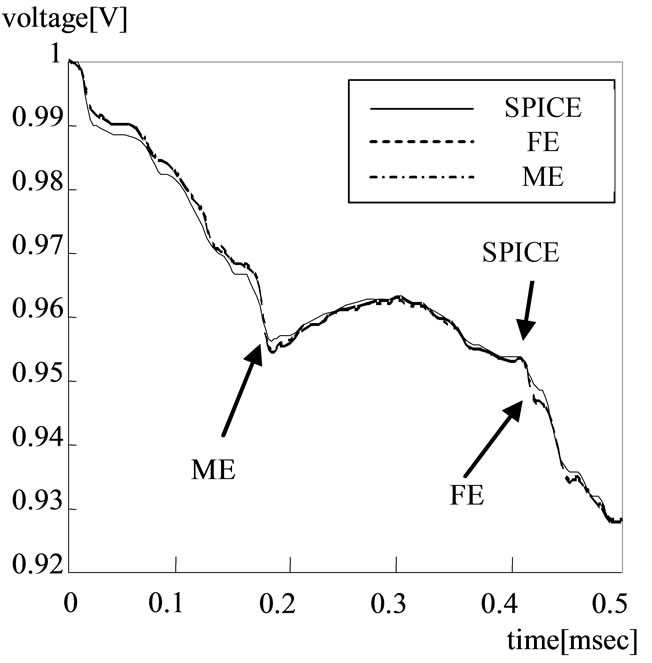
Figure 3. Simulation result by Euler method with small step size.
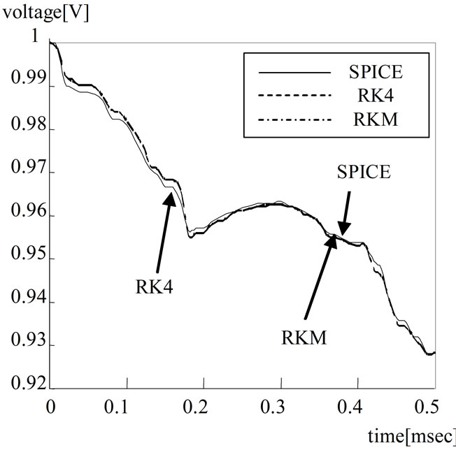
Figure 4. Simulation result by Euler method with small step size.
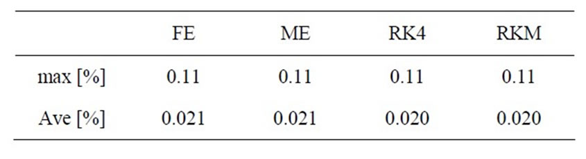
Table 1. Error by fixed point arithmetic for uniform RC circuit.
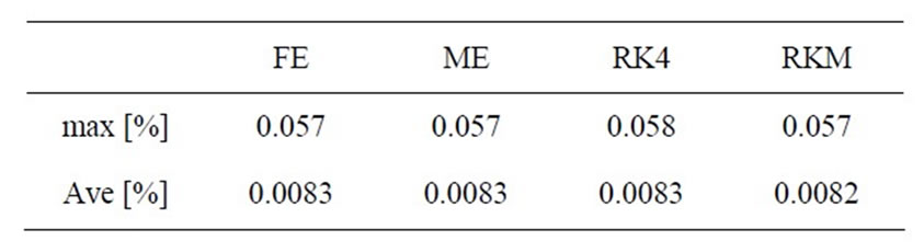
Table 2. Error by fixed point arithmetic for random RC circuit.
combination of the wiring resistance and the capacitance, are executed. Table 2 shows the maximum error and the average error of 100 kinds of circuit selected at random. The high accurate simulation has been achieved with a small time step.
In fixed point arithmetic, fourth order Runge-Kutta Method (RK4) and Runge-Kutta marsun method (RKM) obtain a good result. In addition, the error of uniform RC distribution is larger than that of random circuit. The computational complexity of FE and Modified Euler method (ME) are small. In contrast, RK4 and RKM are complex for computation, though they can execute an accurate analysis.
In our preliminary experiments, FE and RK4 diverged on the same time step. Therefore, FE is superior to RK4 in case of the power grid optimization problem.
2.3.3. Simulation Flow
Voltage and current change in each node at small time step is analyzed based on information of the RC distribution, the current consumption distribution, and the supply voltage, etc. The simulation flow is shown in Figure 5, and a part of the equivalent circuit is shown in Figure 6.
In the simulation part, the current of each wiring is calculated from voltage distribution and the wiring resistance. Then, the charge which accumulates in the capacitance connected with each node is calculated, and the voltage is derived every small time step dT. These processing are iterated during simulation time for entire power grid Tm, and assumed to be end of simulation. To obtain the voltage at each node, the charge is changed by the inflow current Ileft and Iup, the outflow current Iright and Idown, and the current consumption Icon. Voltage and current change in each node are computed based on RC distribution at small time step.
For more high speed simulation, the simulation with hardware is effective, but the achievement of the hardware simulator is not easy according to the restriction of the error margin and the hardware resource. To examine whether it is feasible to make the present simulation hardware, the accuracy of the analysis by the doubleprecision floating point arithmetic and by the single-precision fixed point arithmetic are verified. The error margin is caused by replacing with fixed point arithmetic. It is because the fixed point arithmetic can be processed at the same speed as the integer operation. Additionally, the area of the fixed point arithmetic unit is far smaller compared with the floating point arithmetic unit.

Figure 5. Simulation flow.
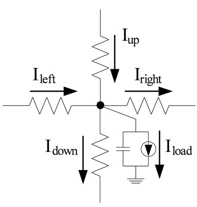
Figure 6. A part of equivalent circuit.
3. Hardware Architecture for Power Grid Simulation
The proposed simulation algorithm adopts fixed point arithmetic. It achieves the same processing speed as the integer operation, and has an advantage of area-efficiency when implementing on hardware. Fixed point arithmetic includes a risk of overflow; however, this risk is reduced by correction processing and bit shift. The simulation part computes the voltage and the current of each node of power grid, and stores the simulation results into memory. Furthermore, it is necessary to control the simulation and the memory behavior to achieve high speed simulation. Figure 7 shows the block diagram of the power grid simulation which corresponds to simulation module and memory access as shown in Figure 2. Control module controls state transition and timing of each module. Each circuit variables are stored in each memory. Wiring resistance and capacitance are updated when changing the circuit design.
The voltage and the charge are updated whenever advancing at a small time step. Therefore, these are stored in RAM. Circuit variables are fetched from the memory into the simulation module, and the results are written into memory.
The simulation module is composed by adder, subtractor, and multiplier, and doesn’t use divider. Current is calculated by dividing potential difference of wiring resistance, however divider needs a lot of implementation areas. Therefore, divider is converted into multiplier by storing each reciprocal when wiring resistance and capacitance are stored in the memory. Figure 8 shows the calculation procedure in the simulation module.
Input variables, “Gright”, “Gdown” and “Z” show the reciprocal of wiring resistance and capacitance respectively. In the current calculation of the hardware algorithm, only outflow current is computed as shown in Figure 4. Because inflow current of a point corresponds to outflow current of the adjacent point (left side or upper side).
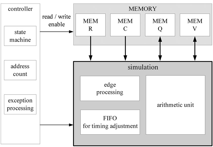
Figure 7. Block diagram of the power grid simulation.
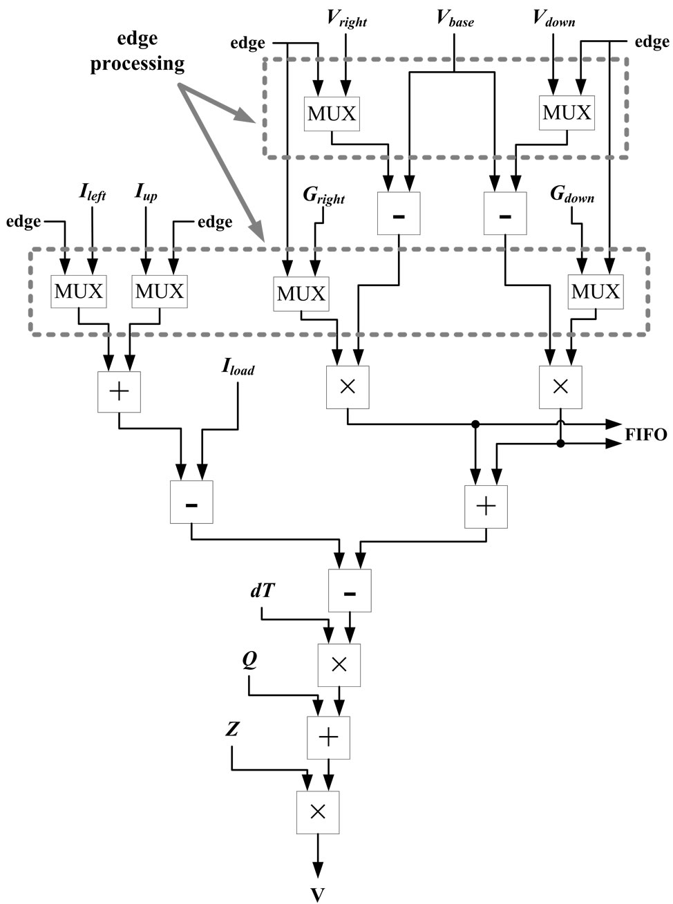
Figure 8. Calculation procedure in the simulation module.
The simulation module processes the circuit variables from memory, and writes simulation result into the memory. The variables written in the memory are the current, the charge, and the voltage. The current is used to calculate the RISK, the charge is necessary for each grid simulation, and the voltage is both. When the edge of the power grid is simulated, the variable is switched to the exception parameter by multiplexer (MUX) because the adjacent SLOT doesn’t exist.
4. Hardware Algorithm
4.1. Pipeline Processing
Registers are inserting between each arithmetic unit to achieve pipeline processing. The proposed pipeline processing is composed of eight stages, and the data of each SLOT is transferred to the simulation module per clock cycle. The simulation flow by pipeline processing is as follows.
1) Each variable is stored from the memory to register.
2) Calculation of potential difference.
3) Calculation of each current.
4) Addition of each current (Iright, Idown, Ileft and Iup).
5) Addition of Stage 4 and current source.
6) Calculation of inflow/outflow currents in small time step.
7) Computation of charge.
8) Computation of voltage.
Figure 9 shows the pipeline stage in the simulation module. All nodes of the power grid are sequentially simulated in the simulation module.
Because current calculation of a node require the voltage of the adjacent node, it is necessary to wait until the adjacent node finishes simulating, even if the node finishes simulating. Horizontal size and vertical size of power grid are defined as H_SIZE and V_SIZE. In an ideal pipeline processing, H_SIZE times V_SIZE clocks are needed for the simulation of all nodes. Moreover, 8 + H_SIZE clocks are needed to finish eight stage pipeline processing of a node and the adjacent node.
4.2. Parallel Processing
Figure 10 shows an example of which a circuit is divided
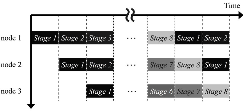
Figure 9. Pipeline stage of each node.
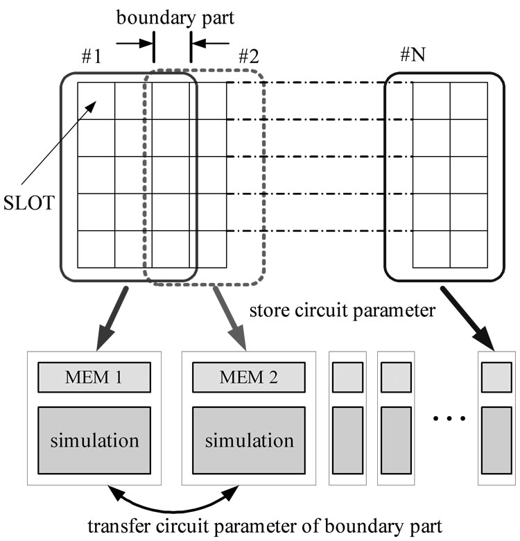
Figure 10. Circuit partitioning for parallel processing.
into N parts to perform parallel processing. The memory and the simulation module are regarded as one functional block, and all the functional blocks are operated in parallel. The boundary of sub-circuit is overlapped, and the data of boundary part is stored in each memory. There is a point that should be considered in parallelization. For example, when simulating the sub-circuit No. 2, voltage is referred from right-hand memory to compute the outflow current of right boundary part. The inflow current is considered to simulate the left boundary part, however the inflow current quotes the outflow current of the left node as shown in Figure 4. However, referring to the inflow current, it is necessary to adjust timing at Stage 2. Then, simulation results are referred from left-hand circuit, and the process of timing adjustment is omitted to prevent performance deterioration. Therefore, the results of boundary part must be stored into each memory.
In massively parallel computing approach, e.g. GPGPU, similar synchronization technique is discussed to hold the important data in shared memories. In our FPGA approach, the structure of the shared memories are structured as we like, thus, in general, more efficient data communications are possible.
5. Experimental Results
5.1. Evaluation of Pipeline Processing
To evaluate the speed of the proposed hardware simulator, FE is described in C language with fixed point, which is functionally equal to the hardware simulator. Bit shift is executed to prevent overflow after multiply operation. The simulation is executed with fixed time step. The FE program in C language is executed on HP xw9400Workstation with Dual-Core AMD Opteron Processor2220 2.8 GHz and 8 GB RAM. The test data for accuracy evaluation is given by an RC circuit as shown in Figure 1, and the circuit scale is 100 × 100 grids. The value of resistance is selected from 2, 3, 4 [mΩ], and the value of each capacitance is selected from 10, 30, 60 [μF].
The supply voltage is 1 [V]. The results of SPICE simulation by the same circuits are used for the reference data. SPICE performs Backward Euler method and Trapezoidal method [14]. These analytical methods realize high accuracy, however take a lot of processing time, in general. For speeding up the simulation, SPICE dynamically selects the time step size. The maximum error ratio in the all node voltage is evaluated by comparing the FE and SPICE.
First, pipeline processing is achieved as one of the speed-up techniques with hardware. The architecture described in Section 4 is achieved with Verilog HDL. Then, the speed performance of the power grid simulation by three processing, software, non-pipeline, pipeline, are compared as shown in Table 3. The processing time of software shows the result of single thread execution. That of HDL is calculated by number of clock times multiplied by the clock period of the FPGA. Target FPGA for logic synthesis is “EP2S180F1020C3, Stratix II, ALTERA”. Quartus II 7.1 is used as a logic synthesis tool. Non-pipeline processing is achieved about 1.2 times faster than software. As a result, the maximum frequency, 26 [MHz], was low because some operations had been executed with one clock. Inserting the register between each arithmetic unit, pipeline processing achieved about three times faster than non-pipeline processing. The maximum clock frequency and the latency are 80 [MHz] and 101 [nsec] by pipeline processing. In this experiment, 32-bit multiplication has become critical path because the pipeline stage was delimited between each arithmetic unit. About dividing the pipeline stage, there is leeway for improvement.
Next, the circuit scale has been changed. Table 4 shows the speed gain by the hardware implementation. Experiment has been executed on large power grid to compare simulation time. The speed gain tends to be high in large scale circuit, and the hardware simulator has achieved 4.5 times faster processing speed than software.
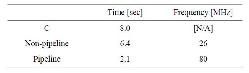
Table 3. Speed gain by pipeline processing.

Table 4. Speed estimation by changing circuit scale.
5.2. Evaluation of Parallel Processing
This section described parallel processing of the power grid simulation. The simulation module by pipeline processing in previous section is connected in parallel. The entire circuit scale is changed from 50 × 50 to 500 × 500, and the speeding gain by the parallel processing is shown in Table 5. Figure 11 shows the processing time and speed ratio when the circuit scale is set to 500 × 500 grids. The bar chart indicates the processing time. The line charts and shows the speeding up ratio when the number of partitions is expanded.
The speeding up ratio is set on the basis of the processing time at one block. A high parallelism have achieved without saturation even if the number of partitions increased. About 7.9 times speeding up has been achieved when the power grid had been divided into eight. When the number of division circuits is defined as N, the speed improvement of proposal algorithm expect as shown in (1).
 (1)
(1)
Increasing the number of division circuit influence speed improvement because the boundary parts are overlapped. Table 6 shows the result of logic synthesis when simulating 100 × 100 grids and divided into eight. The usage rate of DSP is comparatively high. Therefore, it is necessary for higher parallel processing to improve the algorithm or apply to larger scale FPGA.
6. Conclusions
In this paper, we have proposed an efficient hardware circuit simulator for power grid optimization. The proposal technique achieves high accuracy and high speed simulation by adopting fixed point arithmetic and parallel processing.
In the evaluation experiment of accuracy, we have evaluated four type’s analysis method by comparing the
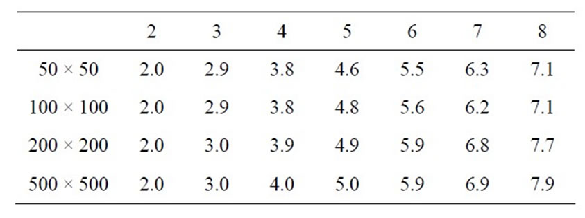
Table 5. Speed gain by changing the number of partitions.
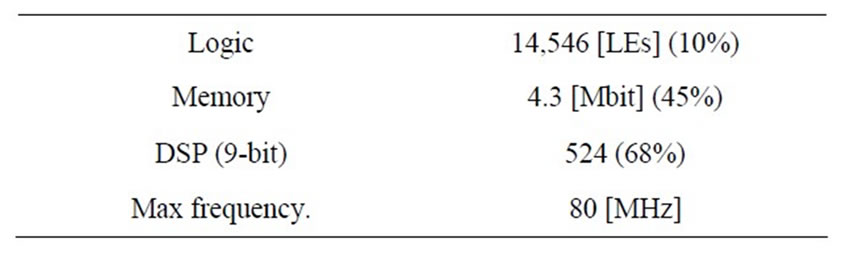
Table 6. Result of logic synthesis of eight parallel simulation modules.
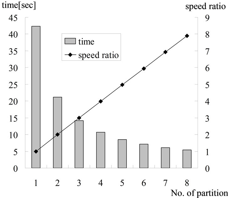
Figure 11. Circuit partitioning for parallel processing.
functionally equal program and SPICE. The FE achieves high accuracy simulation by several different experiments, i.e., in different time steps, floating point or fixed point.
Next, we have evaluated the speed gain by pipeline processing and parallel processing. The proposed power grid simulation algorithm performs 4.5 times faster processing than software processing. In addition, eight parallel processing achieves 7.9 times higher speed than one unit processing. Therefore, the proposed power grid simulation using 80 MHz FPGA achieves 35 times higher speed than software processing with 2.8 GHz CPU while maintaining the high accuracy.
In the future, we will implement the proposed hardware algorithm onto a Compute Unified Device Architecture (CUDA) platform.
REFERENCES
- D. A. Andersson, L. J. Svensson and P. Lasson-Edefors, “Noise-Aware On-Chip Power Grid Considerations Using a Statistical Approach,” Proceedings of International Symposium on Quality Electronic Design, San Jose, 17-19 March 2008, pp. 663-669.
- S. W. Wu and Y. W. Chang, “Efficient Power/Ground Network Analysis for Power Integrity-Driven Design Methodology,” Proceedings of Design Automation Conference, San Diego, 7-11 June 2004, pp. 177-180.
- A. Muramatsu, M. Hashimoto and H. Onodera, “Effects of On-Chip Inductance on Power Distribution Grid,” IEICE Transactions on Fundamentals of Electronics, Communications and Computer Sciences, Vol. E88-A, No. 12, 2005, pp. 3564-3572.
- Y. Zhong and M. D. F. Wong, “Thermal-Aware IR Drop Analysis in Large Power Grid,” Proceedings of International Symposium on Quality Electronic Design, San Jose, 17-19 March 2008, pp. 194-199.
- B. Yu and M. L. Bushnell, “Power Grid Analysis of Dynamic Power Cutoff Technology,” Proceedings of International Symposium on Circuits and Systems, New Orleans, 27-30 May 2007, pp. 1393-1396.
- C. Mizuta, J. Iwai, K. Machida, T. Kage and H. Matsuda, “Large-Scale Linear Circuit Simulation with an Inversed Inductance Matrix,” Proceedings of Asia and South Pacific Design Automation Conference, Kanagawa, 27-30 January 2004, pp. 511-516.
- P. M. Lee, S. Ito, T. Hashimoto, J. Sato, T. Touma and G. Yokomizo, “A Parallel and Accelerated Circuit Simulator with Precise Accuracy,” Proceedings of International Conference on VLSI Design, Bangalore, 7-11 August 2002, pp. 213-218.
- N. Nakasato and T. Hamada, “Acceleration of Hydrosynamical Simulations Using a FPGA Board,” Institute of Electronics, Information and Communication Engineers Technical Report, Vol. 105, No. 515, 2006, pp. 19-24.
- T. Watanabe, Y. Tanji, H. Kubota and H. Asai, “Parallel-Distributed Time-Domain Circuit Simulation of Power Distribution Networks with Frequency-Dependent Parameters,” Proceedings of Asia and South Pacific Conference on Design Automation, Yokohama, 24-27 January 2006, pp. 832-837.
- Y. Gu, T. Vancourt and M. C. Herbordt, “Improved Interpolation and System Integration for FPGA-Based Molecular Dynamics Simulations,” Proceedings of International Conference of Field Programmable Logic and Applications, Madrid, 28-30 August 2006, pp. 1-8. doi:10.1109/FPL.2006.311190
- L. Zhuo and V. K. Prasanna, “High-Performance and Parameterized Matrix Factorization on FPGAs,” Proceedings of International Conference of Field Programmable Logic and Applications, Madrid, 28-30 August 2006, pp. 363-368. doi:10.1109/FPL.2006.311238
- M. Yoshimi, Y. Osana, Y. Iwaoka, Y. Nishikawa, T. Kojima, A. Funahashi, N. Hiroi, Y. Shibata, N. Iwanaga, H. Kitano and H. Amano, “An FPGA Implementation of Throughput Stochastic Simulator for Large-scale Biochemical Systems,” Proceedings of International Conference of Field Programmable Logic and Applications, Madrid, 28-30 August 2006, pp. 227-232. doi:10.1109/FPL.2006.311218
- H. Ishijima, T. Harada, K. Kusano, M. Fukui, M. Yoshikawa and H. Terai, “A Power Grid Optimization Algorithm with Consideration of Dynamic Circuit Operations,” Proceedings of Synthesis and System Integration of Mixed Information, Nagoya, 3-4 April 2006, pp. 446- 451.
- Y. Kawakami, M. Terao, M. Fukui and S. Tsukiyama, “A Power Grid Optimization Algorithm by Observing Timing Error Risk by IR Drop,” IEICE Transactions on Fundamentals, Vol. E91-A, No. 12, 2008, pp. 3423-3430.
- T. Hashizume, H. Ishijima and M. Fukui, “An Evaluation of Circuit Simulation Algorithms for Hardware Implementation,” Proceedings of Synthesis and System Integration of Mixed Information, Hokkaido, 15-16 October 2007, pp. 322-327.