Circuits and Systems
Vol. 3 No. 1 (2012) , Article ID: 16637 , 6 pages DOI:10.4236/cs.2012.31005
Novel Threshold-Based Standard-Cell Flash ADC
1Department of Applied Sciences, Université du Québec à Chicoutimi, Chicoutimi, Canada
2Department of Computer Engineering, École Polytechnique de Montréal, Montréal, Canada
Email: {msiadjine, ht2bui}@uqac.ca, Francois-R.Boyer@PolyMtl.ca
Received October 28, 2011; revised December 1, 2011; accepted December 10, 2011
Keywords: Flash ADC; Standard Cells; Data Converters
ABSTRACT
This paper introduces a novel standard-cell flash architecture for implementing analog-to-digital converters (ADC). The proposed ADC consists of several CMOS inverters all having their inputs connected to a common input node. The output of the ADC is a thermometer code generated by the inverter outputs. Depending on the relationship between the input signal and a given inverter’s threshold voltage, the output will either be “0” or “1”. By having many inverters with different threshold voltages, it is possible to create a 3-bit flash ADC. Even though the system is inherently non-linear, mathematical optimization has been done in order to improve its linearity. The proposed circuit dissipates 6.7 mW and uses in total 672 transistors of PMOS and NMOS types. This ADC is designed and simulated using TSMC’s 0.18 μm CMOS and results show that the proposed circuit works as expected even in presence of process variations.
1. Introduction
The aggressive technology scaling seen in recent years has helped improve the performance of many digital systems. Analog systems, on the other hand, have not benefited as much, as they are more sensitive to process variations which become more dominant with smaller technology nodes. In addition, reduction in feature size often entails reduction in supply voltage which can also cause problems in the design of analog circuits. These are some of the reasons why designers are interested in moving certain modules from the analog domain into the digital domain. Perhaps the most significant example is filters. Since passive components need certain physical dimensions in order to have the desired behavior, they do not scale down very well with node size reduction. That is the reason why many filters have migrated into the digital domain [1,2].
In order to convert analog modules into digital modules, ADC and digital to analog converters (DAC) are typically required to interface between the domains. The design of these components typically requires a certain level of expertise and they also require analog/mixed signal components. These two points typically increase the required design time and also increase the risk of having non-functional designs. It is therefore interesting to investigate ways to migrate these designs into more digital forms by using standard-cells [2-5]. Furthermore, a flash ADC which is mainly known for its high-speed conversion rate [6,7] consumes more power and occupies larger chip area in comparison to the other types of ADCs such as Successive Approximation and pipelined ADCs [8,9].
In this paper, we propose a flash ADC that can be fully implemented using only standard-cells. This approach helps to improve the high-speed conversion rate while maintaining comparable power consumption. This allows also the designer to stay within the mature digital design flow and effectively reduce risks and time-to-market. Other benefits of using this approach include higher speed and simpler design implementation.
The rest of the paper is divided as follows. Section 2 introduces the basic concept along with a first version of the proposed ADC. A second version with increased linearity and modularity is presented in Section 3. Design and simulation results of the implemented circuits are shown in Section 4 and conclusions are drawn in Section 5.
2. Initial Architecture
ADCs are an important building block in modern electronic systems. While numerous architectures exist [10- 12], this work mainly focuses on the flash ADC whose structure is shown in Figure 1(a).
The circuit in Figure 1(a) uses a string of resistors and comparators to generate a thermometer code in response to an analog input. The ADC shown in Figure 1(a) can be converted into a standard-cell form if the resistors and the comparators were substituted by logic gates Figure
 (a)
(a)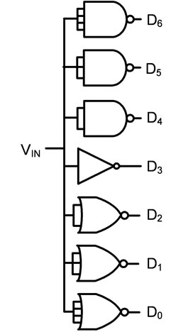 (b)
(b)
Figure 1. (a) Circuit of a flash ADC and of (b) the proposed architecture.
1(b). The proposed flash architecture uses logic gates configured as inverters that have different threshold voltages. The threshold voltage of the gates serves as the reference voltage to which is compared the input.
To explain the principle of operation, let us consider a 2-input NAND gate whose inputs are connected together. In such a configuration, the gate operates much like an inverter. The difference, however, lies within the threshold voltage of the gate. In a NAND gate, the NMOS network is in series whereas the PMOS network is in parallel. If the NMOS and the PMOS gates had identical VTH and were sized to have identical μCOX (W/L), the threshold of the NAND would be higher than that of the inverter. This is because, for the same VGS, the PMOS network would generate more current since it has a parallel connection whereas the NMOS network has a series connection. For the currents to be equal, the NMOS transistors would need to have higher VGS which explains the rise in gate’s threshold voltage. A similar reasoning can be applied to a 2-input NOR gate and the conclusion would be that its threshold voltage is lower than that of the inverter.
To calculate the value of these threshold voltages, let us define the threshold voltage of a logic gate as being the input voltage at which the output voltage is VDD/2. To simplify the analysis, we will assume that identical transistors in series can be considered as a single transistor whose channel is longer. Similarly, when identical transistors are in parallel, we assume that they can be seen as one transistor whose channel is wider.
For the purpose of this analysis, let us only consider inverters, NAND gates and NOR gates. Let M be the number of NMOS transistors connected in parallel. Knowing that static gates are complementary, the P-network will then have M transistors in series. The NMOS transistors can be replaced by a single transistor having a width that is M times that of that of the original transistor. Similarly, the PMOS transistors can be replaced by a single transistor having a length that is M times that of that of the original transistor. This simplification facilitates the task of writing the current equation. However, equations cannot be written until the region of operation of these transistors is determined. Knowing that the threshold of a gate is the input voltage that generates an output of VDD/2, it is mandatory that all PMOS and NMOS be conducting. This condition is satisfied when:
 (1)
(1)
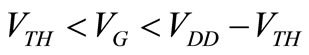
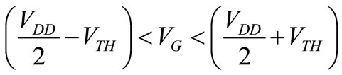
In addition, we know that the NMOS will be in saturation when VDS > VGS – VTH. Since VDS is equal to VDD/2 at the threshold voltage, VGS needs to be smaller than VDD/2 + VTH for the transistor to be in saturation. Similarly, the PMOS is in saturation when VSD is greater than VSG-VTH. Since VSD is equal to VDD/2 at the threshold voltage, the PMOS is in saturation when VDD/2 > VDD – VG – VTH. Thus, both networks will be in saturation if the following condition is satisfied:
 (2)
(2)
It can be shown that when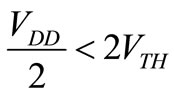 , both conditions in Equations (1) and (2) will be simultaneously satisfied. In this case, it means that, at the threshold voltage of the gate, all transistors will be in saturation. The technology used for this work meets all aforementioned conditions and therefore, the transistors will always be in saturation near the threshold voltage of the gate. Knowing the region of operation of these transistors, and knowing that their current is equal, it is possible to write the following equation:
 (3)
(3)
When Equation (3) is solved for VG, the threshold voltage of the gate (known as VGTH) is obtained:
 (4)
(4)
Equation (4) shows how the threshold voltage of a gate changes as a function of M. By using NAND and NOR gates with higher fan-ins, the value of M changes which, in turn, changes the threshold voltage of the gate. It is therefore possible to create a set of inverters having different threshold voltages to create a flash ADC using only standard cells.
To validate the functionality of the proposed architectture, a sample 3-bit ADC was created using a MATLAB model, version 2007. This architecture consists of NAND and NOR gates with two, three and four inputs along with an inverter (Figure 1(b)). Recall that M is the number of NMOS transistors connected in parallel. When these NMOS are connected in series, the value of M will be inverted. For instance, M will be equal to 1/4 for a 4-input NAND gate whereas it will be equal to four for a 4-input NOR gate. For the case of an inverter M will be equal to one.
By using TMSC’s 0.18 m CMOS technology parameters in our MATLAB model, the different values of VGTH have been plotted as function of M and the results are shown in Figure 2. The ideal ADC relationship between the input and output is also shown in the figure as a dotted line.
This figure shows that the relationship between M and threshold voltage is monotonic but clearly not linear. To quantify the linearity of the ADC, it is possible to use the sum of squared error between the real and ideal threshold voltages. In this sample implementation, the sum of squared error is calculated to be:

In this equation, n is the index value representing M whereas VnIDEAL and VnADC are respectively the ideal and calculated threshold voltage.
3. Architecture with Improved Linearity
The previous section introduced a standard-cell flash ADC that works properly but lacks linearity. In this section, we propose a second design that is more modular and has improved linearity at the expense of a larger area and increased power consumption. The proposed architecture is shown in Figure 3. It consists of NAND and NOR gates of the highest fan-in in a given standardcell library. For the purpose of explaining the architecture, let us consider gates with a fan-in of four. The number of gates used in this structure will be equal to (2N – 2) * (2N – 1), where N is the number of bits in the ADC. By progressively changing the number of NAND and NOR gates per output, it is possible to have threshold voltages that are more linearly spaced. An implementation with Q

Figure 2. Plot of the threshold voltage as a function of m.
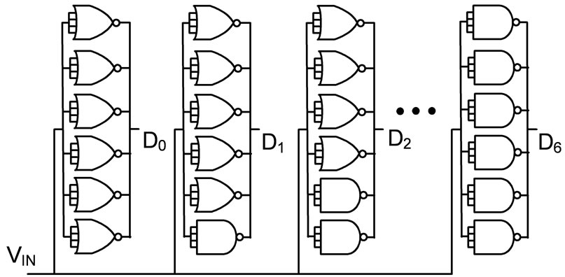
Figure 3. Architecture of the 3-bit ADC with Q = 6.
= 6 is shown in Figure 3, where Q and P are respectively the total number of gates and the number of NOR gates per output.
To calculate the linearity of the proposed ADC with Q equal to six, we must first calculate the threshold voltage of the different block of gates (D0 to D6). This is done by writing the current equations for the N-network and the P-network:
 (5)
(5)
 (6)
(6)
By equating (5) and (6) and by solving for VG, we can find the threshold voltage of the different block of gates. The resulting equation for the threshold voltage is large and will therefore not be written here. Instead, its value has been calculated with the chosen process parameters and the results are plotted in Figure 4.
A comparison between Figure 4(a) and Figure 4(b) shows that the linearity has been improved. In order to quantify the improvement in linearity, the sum of squared error has been calculated:

These results show that this new architecture is about three times more linear than the architecture proposed in the previous section.
3.1. Optimization
In order to further improve the linearity of the proposed solution, it is possible to increase Q to a value higher than (2N – 2). For instance, by doubling the value of Q while still keeping the number of bits equal to N, the result is a structure that has more threshold voltages than what is required. By selecting only the (2N – 1) required
 (a)
(a)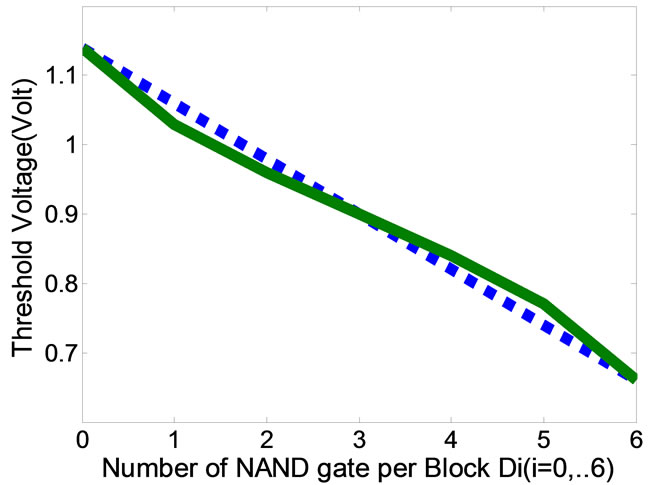 (b)
(b)threshold voltages and by discarding the other possibilities, it is possible to improve the linearity of the ADC. The heuristic algorithm used for this process is described in the following pseudo-code:
NumberNAND(i) = 0 i
For i = 0 to 7
set NumberNAND(i)  [0, 12]
to minimize (idealvth(i) − adcvth(i, NumberNAND))2
End
To test the effectiveness of the proposed algorithm, it was applied to optimize the 3-bit ADC proposed in Figure 3. During this process, the squared errors were calculated and plotted for each of the associated block of gates in Figure 3. A sample plot is presented in Figure 5 which shows the change in the sum of squared error as the number of NAND gates per block is changed. By using the number of NAND gates that minimizes the squared error for each block, it is possible to have a more linear ADC.
In Figure 5, it can be seen that, to minimize the error, the block of gates associated to D2 must contain three NAND gate. The other blocks were analyzed the same way to determine the number of NANDs to include.
Using this configuration, the threshold voltage of the proposed ADC was calculated and the results are shown in Figure 6. It shows a relation that is more linear than that of Figure 4.
To quantify the linearity, we used the sum of squared error:

This error is about 9.1% of its original value and validates the approach used during the optimization process.
3.2. Characterization
The proposed 3-bit ADC is designed in 180nm technology, characterized for parameters like differential nonlinearity (DNL), integral non-linearity (INL) as shown in Figure 7. The results show that the ADC exhibits a maximum DNL of 0.4 LSB and INL of 0.2 LSB respectively.
4. Transistor-Level Design
To verify the functionality and the effectiveness of the proposed ADCs, these circuits were designed at the transistor level using 0.18 μm CMOS technology and simulated using Cadence’s Spectre simulator. For the purpose of this test, two circuits were created: the original design (Figure 1(b)) and the design with improved linearity (Figure 3) that has also been optimized. The two circuits were evaluated by injecting a slow ramp at the input and observing the point at which the outputs toggle. The result
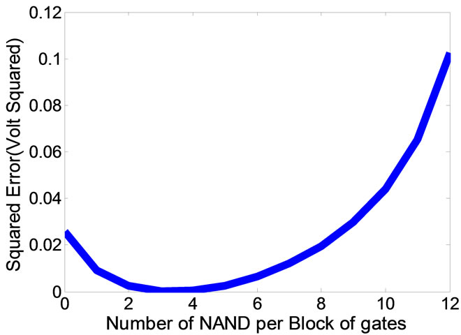
Figure 5. Sum of squared error for the D2 block.

Figure 6. Threshold voltage of optimized blocks of gates.
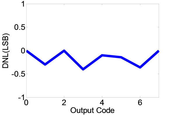
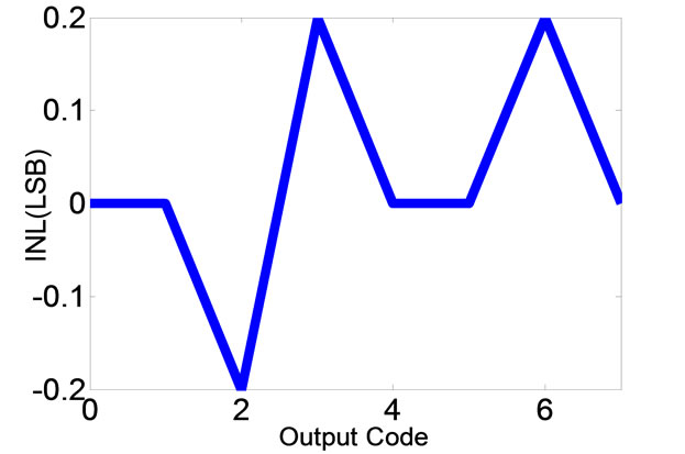
Figure 7. DNL and INL graphs of the proposed flash ADC.
of this simulation is shown in Figure 8. Figure 8(a)) shows the output of the original 3-bit ADC whereas Figure 8(b)) shows the output of the optimized design. These figures show that, as the input voltage increases, it eventually surpasses the value of the different reference voltages, which makes the gates transition to from “0” to “1”. It confirms that the proposed ADCs operate as expected.
From these figures, it is also possible to see that the spacing between the transitions in Figure 8(a) is more uniform than the spacing from Figure 8(a). This implies that the optimized design is more linear than the original one. To visualize the linearity of the proposed circuits, the simulation results have been measured and tabulated. These results were used to create Figure 9.
In this figure, the dotted line is the ideal response; the solid line with the markers is the original design whereas the remaining trace is the optimized design. It shows that the optimized design has a much more linear response.
To verify the proposed circuit’s robustness to process variations, Monte Carlo analysis was run on the design for 100 cycles and no shown in this paper. The evaluated parameter in these simulations is the difference between adjacent reference voltages and. The simulation indicated that all the reference voltages typically change in the same direction in presence of process variations. Therefore, even in presence of process variations the difference in reference voltages varies minimally which ensures that the ADC will work even under process variations.
5. Conclusion
In this paper, we introduced a novel threshold-based standard-cell flash ADC. Its implementation is fully
 (a)
(a) (b)
(b)
Figure 8. Responses of the (a) Original and of the (b) Optimized ADCs.

Figure 9. Linearity of the proposed ADCs to a ramp input.
compatible with standard digital CMOS technology. The functionality of the proposed design was demonstrated using basic current equations. A new architecture with an enhanced linearity was also proposed. A linearization heuristic based on the sum of squared errors was introduced in order to improve its performance. It is shown that the resulting design is more linear. To validate the results, transistor-level simulations have been executed using Cadence’s Spectre simulator while Monte Carlo simulations show that a 3-bit resolution is possible in 0.18 μm CMOS technology.
6. Acknowledgements
The authors would like to acknowledge financial support from NSERC and ReSMIQ.
REFERENCES
- S. Y. Sedra and K. C. Smith, “Microelectronic Circuits,” Fourth Edition, Oxford University Press Inc., Oxford, 1998.
- T. Watanabe, T. Mizuno and Y. Makino, “An All-Digital Analog-to-Digital Converter with 12-µV/LSB Using Moving-Average Filtering,” IEEE Journal of Solid-State Circuits, Vol. 38, No. 1, 2003, pp. 120-125. doi:10.1109/JSSC.2002.806263
- D. Lee, et al., “Design Method and Automation of Comparator Generation for Flash A/D Converter,” ACM Portal, No. 5, 2004, pp. 127-155.
- H. Farkhani, M. Meymandi-Nejad and M. Sachdev, “A Fully Digital ADC Using a New Delay Element with Enhanced Linearity,” IEEE International Symposium on Circuits and Systems, ISCAS, 18-21 May 2008, pp. 2406- 2409. doi:10.1109/ISCAS.2008.4541940
- M. A. Farahat, F. A. Farg and H. A. Elsimary, “Only Digital Technology Analog-to-Digital Converter Circuit,” International Midwest Symposium on Circuits and Systems, IEEE, Vol. 1, 2003, pp. 178-181.
- B. Yu and W. Black Jr., “A 900 MS/s 6 b Interleaved CMOS Flash ADC,” IEEE Custom Integrated Circuits Conference, Vol. 8, 2001, pp. 149-152.
- G. Geelen, “A 6 b 1.1 GSample/s CMOS A/D Converter,” IEEE International Solid-State Circuits Conference, San Francisco, Vol. 2, 5-7 February 2001, pp. 128- 129. doi:10.1109/ISSCC.2001.912572
- H. Chen, B. Song and K. Bacrania, “A 14-b 20-M Samples/s CMOS Pipelened ADC,” IEEE Journal of SolidState Circuits, Vol. 6, 2001, pp. 997-1001. doi:10.1109/4.924862
- Y. Park, S. Karthikeyan, F. Tsay and E. Bartolome, “A 10 b 100 M Samples/s CMOS Pipelined ADC with 1.8 V Power Supply,” IEEE International Solid-State Circuits Conference, Vol. 8, 2001, pp. 130-131.
- J. Lin and B. Haroun, “An Embedded 0.8V/480μW 6b/22MHz Flash ADC in 0.13 μm Digital CMOS Process Using Nonlinear Double-Interpolation Technique,” IEEE Journal of Solid-State Circuits, Vol. 37, No. 12, 2002, pp. 1610-1617. doi:10.1109/JSSC.2002.804333
- F. Munoz, A. P. VegaLeal, R. G. Carvajal, A. Torralba, J. Tombs and J. Ramirez-Angulo, “A 1.1 v Low-Power ΣΔ Modulator for 14-b 16 KHz A/D Conversion,” IEEE International Symposium on Circuits and Systems, Vol. 1, 2001, pp. 619-622.
- B.-S. Song, “Analog Front-End Macro Circuit Design,” International Symposium on VLSI Technology Systems and Applications, Taipei, 8-10 June 1999, pp. 223-226. doi:10.1109/VTSA.1999.786040