Journal of Modern Physics
Vol.4 No.2(2013), Article ID:27721,5 pages DOI:10.4236/jmp.2013.42025
Space Environment Simulator for Testing of Materials and Devices
1A.I. Alikhanyan National Science Laboratory, Yerevan Physics Institute, Yerevan, Armenia
2Institute of Metrology of Armenian Republic, Yerevan, Armenia
Email: *grant@yerphi.am, metrology@metrology.am
Received November 29, 2012; revised December 31, 2012; accepted January 8, 2013
Keywords: Space; Silicon; Radiation Defects (RD); Conductivity; Carrier Concentration
ABSTRACT
Equipment has been designed and created for experimental simulation of space environment conditions of Geostationary orbit of the Earth. The following conditions are supported in the vacuum chamber having volume of 1.2 cubic meters: Vacuum 10−5 Torr. (1.3 × 10⁻³ Pa), electron beam with energy up to 8 MeV, temperatures from −150˚C to +150˚C and solar ultraviolet radiation. The peculiarity of this equipment is the possibility of analyzing complex simultaneous influence of mentioned above 4 factors on the sample and in-situ direct measurement of sample parameters under irradiation which provides almost real conditions. Silicon single crystals used in space environment were tested in the vacuum chamber and new results were received having scientific and applied interest. It was shown, particularly, that the electro-conductivity of silicon samples has higher value at in-situ condition than ex-situ after irradiation.
1. Introduction and Objectives
Nowadays the Space science is one of those fields that attract the highest attention from research institutes, industry and even governments. Moreover, it is a more global problem including the interests of all countries. Hence, the study of materials and devices in the environment close to space can play an important role in research and technology, in particular, as to create materials and devices with new or improved functions used in space conditions (for example, high particles irradiations). Beyond its strong link with materials science, it contributes to the development of new components, new systems for devices applicable in space and other fields ranging from production engineering to control system and measurement techniques. The advances in space technology require creation of new base elements with small sizes. The use of irradiation methods allows to work out, for example, nano-materials which are very important in this regard.
The fast growing interest in space sciences and number of publications [1-5], require comprehensive discussion and understanding of the results of investigations, in particular, in-situ research which reflects the real situation.
The present work is an attempt to summarize some physical conditions corresponding to space environment (extreme physical conditions), which impact properties of materials and devices located on the outer surface of the satellite.
2. Experimental Methods and Equipment
For study of mentioned above problems a new experimental facility (with special hall) was designed and created in Yerevan Physics Institute for studying the properties of materials and devices at the extreme physical conditions of: different temperatures, high vacuum (about 10−5 Torr.), electron irradiation (energy 8 MeV, different doses), solar UV radiation. Following experimental methods are applied: Hall Effect and electrical conductivity standard measurements (their temperature dependences). The design of the facility simulating near Earth space environment (SES) is presented in Figures 1-3.
Low temperatures up to 100 K in the vacuum chamber are achieved by liquid nitrogen evaporation through copper tubes welded in the vacuum chamber so that the electron beam and ultraviolet radiation do not catch their surface. Besides, the incidence angles of these beams are mounted so that the testing sample is under these beams simultaneously. The sample irradiation area is 60 mm × 400 mm and its movement is provided by step motor with step of 0.5 mm. High temperatures may be achieved by electron beam influence in the vacuum conditions.
The created SES allows to choose one of 4 mentioned space factors and to study the sample property separately or together at their simultaneous influences. The electron irradiation and vacuum conditions have been chosen in this experiment and electro-physical parameters of n type silicon (n-Si) single crystals (mostly using in electronic industry) were measured in-situ and ex-situ conditions. The samples with specific resistance of 4 kΩ∙cm and 100 Ω∙cm have following sizes: thickness 0.4 mm; width 4 mm, length 10 mm and distance between contacts 5 mm. Note, that the sample of 4 kΩ∙cm has highest sensitivity to the irradiation while the sample of 100 Ω∙cm is mostly used in electronic industry. The temperature at the vacuum chamber during these experiments was about +150˚C.
The conductivity was measured at in-situ process only, while at ex-situ process other electro-physical parameters were measured as well. The conductivity, mobility and carrier concentration were measured by Hall Effect equipment having following parameters: magnetic field induction 0.3 Tesla; Hall-potential and contact differential voltage were measured by voltmeter B7-34A (Russian production) with input impedance of 2 × 10 Ω and accuracy of 5%. The Ohmic contacts were made by Ga:Zn compound with relation 1:4. In-situ measurements were performed at the distance of 1 m from the exit window of the linear accelerator. Electron beam current from linear accelerator has pulse form with length of 5 μsec and frequency of 200 Hz. The electron irradiation current was indicated by the “Faraday cap” and irradiation dose was determined by D = It/S × 6.25 × 10¹² el/cm2, where I is the mean current of the beam in μA, texposure time in seconds, S-cross section of the beam in cm2. The using of low intensity of electron irradiation allowed to apply low dose irradiations with high accuracy.
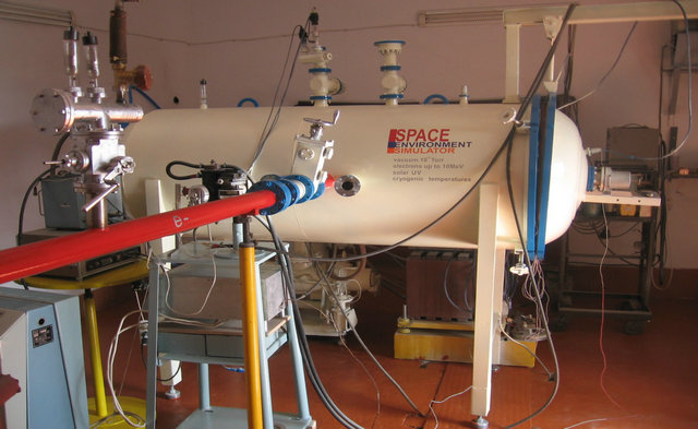
Figure 1. General view of SES.
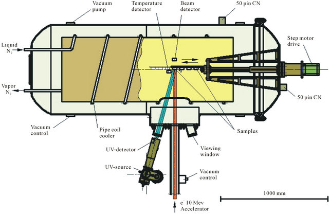
Figure 2. Horizontal section of SES.
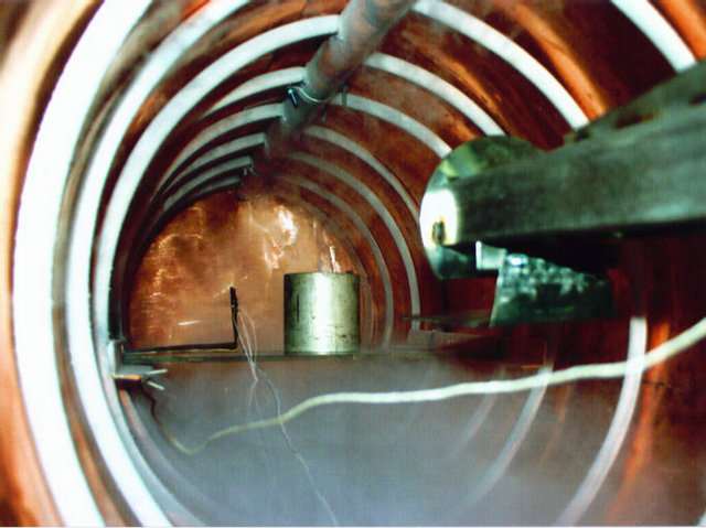
Figure 3. Inner part of vacuum chamber.
3. Results and Discussion
The measurements results versus electron radiation dose for both silicon samples are presented in Figures 4-10.
Figure 4 presents electron irradiation dose dependence (different intensity) of silicon sample conductivity. First of all, n-p conversion is observed (for all 3 used irradiation intensities) at very low irradiation intensities and doses, which in this picture is very narrow and we did more comprehensive measurements extending this region (Figure 5). It is obvious from Figure 5 that the Si conductivity after n-p conversion trends to saturation at all given irradiation intensities. Besides, Si conductivity differs almost 8 times for presented intensities and it increases with irradiation intensity increasing at the same irradiation dose. It means that although the physical nature of dose dependence of conductivity is the same for given intensities, there is an additional mechanism influencing the conductivity. In our mind this may be the result of additional electron-hole pair production at higher irradiation intensities.
Electron irradiation dose dependence of conductivity of n-Si with specific resistance of 4 kΩ∙cm is given in Figure 5 at very narrow region and low intensity (about 100 times lower than in Figure 4). In this case the values of conductivity at in-situ and ex-situ conditions are almost the same. The ex-situ comprehensive measurements allowed defining exact value of irradiation dose where n-p conversion occurs. Besides, the irradiation dose dependence of conductivity shows its decreasing with increase of irradiation dose which corresponds to known results [6-8], when so called A-centers (oxygen atom + vacancy) are formed in Si crystals and radiation compensation takes place. This statement is confirmed in Figures 6 and 7, where the irradiation dose dependences of charge carriers concentration and their mobility are presented, respectively. It is obvious from Figure 7 that the irradiation dose dependence of charge carriers’ con-
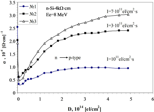
Figure 4. Electron irradiation dose dependence (for different irradiation intensity I) of conductivity of n-Si with specific resistance of 4 kΩ∙cm in-situ measurements.
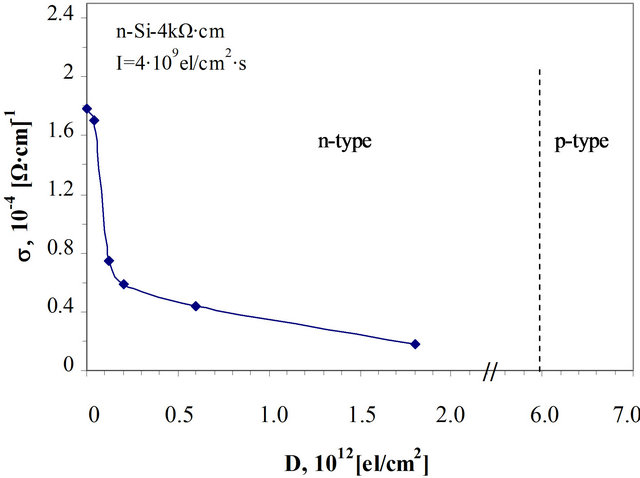
Figure 5. Electron irradiation dose (at very narrow region and low intensity) dependence of conductivity of n-Si with specific resistance 4 kΩ∙cm In this case the values of conductivity at in-situ and ex-situ conditions are almost the same.
centration has the same character as the conductivity and this defines the behavior of electrical property of Si. Although the behavior of Hall mobility of charge carriers looks like the conductivity, too, its dose dependence is weak. Besides, there is a little maximum which may be due to so called “low dose effect”. Thus, the experiments for n-Si with specific resistance 4 kΩ∙cm show that these samples are very sensitive to the irradiation by electrons and the irradiation dose dependence of conductivity has known behavior as ex-situ even in-situ process [9-11].
The behavior of n-Si with specific resistance 100 Ω∙cm is presented in Figures 8-10. Figure 8 shows electron irradiation dose dependence of conductivity for these samples at in-situ and ex-situ processes. It is obvious that in the first case the conductivity is much higher than in the second case and it has maximum value (more
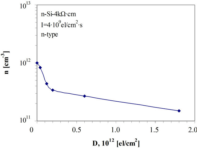
Figure 6. Electron irradiation dose (at very narrow region and low intensity) dependence of charge carrier concentration of n-Si with specific resistance of 4 kΩ∙cm. Ex-situ measurements.
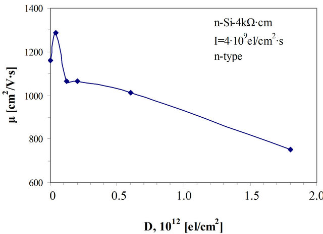
Figure 7. Electron irradiation dose (at very narrow region and low intensity, about 100 times lower than in Figure 4) dependence of charge carrier mobility of n-Si with specific resistance of 4 kΩ∙cm. Ex-situ measurements.
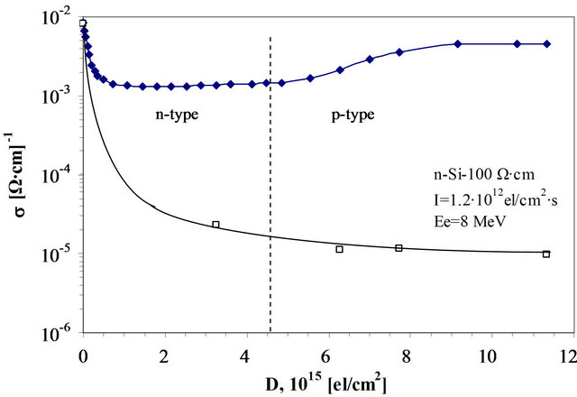
Figure 8. Electron irradiation dose dependence of conductivity of n-Si with specific resistance of 100 Ω∙cm. The solid cubic refers to in-situ while the empty-to ex-situ situations.
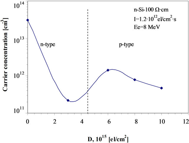
Figure 9. Electron irradiation dose dependence of carrier concentration of n-Si with specific resistance of 100 Ω∙cm. Ex-situ measurements.
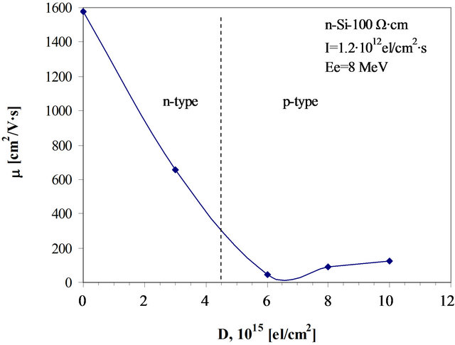
Figure 10. Electron irradiation dose dependence of carrier mobility for n-Si with specific resistance of 100 Ω∙cm. Exsitu measurements.
than factor 100) at irradiation dose of 1.2 × 10¹⁶ el/cm2. Besides, the observed n-p conversion is not sharp as for samples with 4 kΩ∙cm although the behavior of irradiation dose dependences of electrical parameters is almost the same. Figure 9 presents electron irradiation dose dependence of charge carriers’ concentration which is almost similar to Figure 6 at n-region of conductivity. The difference is only in values of the carriers’ concentrations and irradiation doses, i.e., the same physical phenomena take place in both samples with different specific resistance. In our opinion, it is a result of radiation defect production in Si crystals.
It is known, that the irradiation by electron with energy 8 MeV forms in Si crystals structural point radiation defects (RD) and complex defects (in particular, with impurity), so called “secondary radiation defects” (SRD) [8,9]. At low irradiation doses mainly point defect production may occur [7], while at high doses and intensities, the SRD formation becomes preferable, and moreover, it is probable of clusters forming, too [5]. In these experiments the electrons with used energy and irradiation doses do not form cluster type radiation defects and it is considered mainly as SRD production, known as A-centers, (interstitial oxygen atom + Si-vacancy) and E-centers (donor atom + Si-vacancy).
Generally, the introduction of RD leads to reduction of concentration of main carrier concentration and their mobility in Si crystal. The degree of variation of these parameters depends on initial properties of the Si-samples (impurity content, defect structure), energy, dose and intensity of irradiation. Energetic levels of RD in the forbidden gap of n-Si have been determined according to thermal dependence of carrier concentrations at different irradiation doses taking into account the capture probability of vacancies by matrix and non-matrix atoms which stimulate conductivity because the carriers’ mobility has a weak dose dependence.
4. Conclusions
The results bring to following conclusions:
• Electron irradiation induces into Si different RD, concentration and character of which highly depends on dose and intensity of radiation.
• The higher value of electro-conductivity under the irradiation process (in-situ) is due to ionization mechanisms which result in the formation of non-equilibrium carriers (hole-electron pairs).
• Different radiation intensity at the same dose may result in differences of electro-physical properties of the materials (as demonstrated in this paper for Si). This is important for space applications because in such tests only irradiation dose is taking into account. Hence, it is necessary to establish some international radiation intensity standard for accelerating the ground tests radiation experiments compared with space intensities which are 100 - 1000 times lower. Because of it is impossible to operate ground radiation sources continuously for months and years.
• This work demonstrates the importance of in-situ study of radiation defect production in solids which describe the results in real situation.
REFERENCES
- S. Duzellier, “Radiation Effects on Electronic Devices in Space,” Aerospace Science and Technology, Vol. 9, No. 1, 2005, pp. 93-99. doi:10.1016/j.ast.2004.08.006
- A. I. Akishin, “Kosmicheskoe Materialovedenie (Space Material Science),” Moscow State University Publication, Moscow, 2007.
- C. Leroy and P.-G. Rancoita, “Particle Interaction and Displacement Damage in Silicon Devices Operated in Radiation Environments,” Reports on Progress in Physics, Vol. 70, No. 4, 2007, pp. 493-625. doi:10.1088/0034-4885/70/4/R01
- V. B. Molodkin, S. I. Olikhovskii, E. G. Len1, B. V. Sheludchenko1, et al., “X-Ray Diffraction Characterization of Microdefects in Silicon Crystals after High Energy Electron Irradiation,” Physica Status Solidi (A), Vol. 208, No. 11, 2011, pp. 2552-2557. doi:10.1002/pssa.201184253
- V. V. Emtsev, A. M. Ivanov, V. V. Kozlovski, A. A. Lebedev, G. A. Oganesyan, N. B. Strokan and G. Wagner, “Similarities and Distinctions of Defect Production by Fast Electron and Proton Irradiation: Moderately Doped Silicon and Silicon Carbide of n-Type,” Fizika i Tekhnika Poluprovodnikov, Vol. 46, No. 4, 2012, pp. 473-481.
- B. N. Mukashev, K. A. Abdullin and Y. V. Gorelkinski, “Metastable and Bistable Defects Isilicon,” Uspekhi Fizicheskikh Nauk, Vol. 170, No. 2, 2000, pp. 143-154. doi:10.3367/UFNr.0170.200002b.0143
- S. Makhkamov, N. A. Tursunov, M. Ashurov, R. P. Saidov and Z. M. Khakimov, “Formation of Radiation Defects in Silicon Structures under Low Intensity Electron Irradiation,” Semiconductor Science and Technology, Vol. 16, No. 7, 2001, pp. 543-547. doi:10.1088/0268-1242/16/7/303
- V. S. Vavilov, “Atomic Migration and Defect Concentration and Structure Changes Due to Electronic Subsystem Excitations in a Semiconductor,” Uspekhi Fizicheskikh Nauk, Vol. 167, No. 4, 1997, pp. 407-412. doi:10.3367/UFNr.0167.199704c.0407
- G.-F. Chen, W.-B. Yan, H.-J. Chen, H.-Y. Cui and Y.-X. Li, “Infrared Studies of Oxygen Related Complexes in Electron-Irradiated Cz-Si,” Chinese Physics B, Vol. 18, No. 7, 2009, p. 2988. doi:10.1088/1674-1056/18/7/061
- K. D. Shcherbachev, V. T. Bublik, V. N. Mordkovich and D. M. Pazhin, “The Effect of in Situ Photoexcitation on the Generation of Damaged Structures during Ion Implantation into Si Wafers,” Journal of Physics D: Applied Physics, Vol. 38, No. 10A, 2005, pp. A126-A131. doi:10.1088/0022-3727/38/10A/024
- P. C. Srivastava, O. P. Sinha, J. K. Tripathi and D. Kabiraj, “In Situ I-V Study of Swift (~100 MeV) O6+ IonIr-radiated Pd/n-Si Devices,” Semiconductor Science and Technology, Vol. 17, No. 9, 2002, pp. L44-L46. doi:10.1088/0268-1242/17/9/102
NOTES
*Corresponding author.