Journal of Modern Physics
Vol.3 No.7(2012), Article ID:21098,8 pages DOI:10.4236/jmp.2012.37074
Annealing Effects on Electrical Properties and Interfacial Reactions of Ni/Cu Schottky Rectifiers on n-Type InP
1Department of Physics, SSBN Degree and PG College, Anantapur, India
2Department of Physics, Rayalaseema University, Kurnool, India
3Department of Physics, Sri Venkateswara University, Tirupati, India
Email: *ymkredi@gmail.com
Received April 22, 2012; revised May 18, 2012; accepted June 15, 2012
Keywords: Schottky contacts; n-type InP; I-V characteristics; structural properties; X-ray diffraction; SEM
ABSTRACT
We report on the effect of annealing temperature on electrical, interfacial reactions and surface morphological properties of Ni/Cu Schottky contacts on n-type InP. The extracted barrier height of as-deposited Ni/Cu Schottky contact is 0.59 eV (I-V) respectively. The high-quality Schottky contact with barrier height and ideality factor of 0.65 eV (I-V) and 1.15 respectively, can be obtained after annealing at 300˚C for 1 min in a nitrogen atmosphere. However, annealing at 400˚C, results the decrease in the barrier height to 0.54 eV (I-V). From the above observations, it is observed that Ni/Cu Schottky contact exhibited excellent electrical properties after annealing at 300˚C. Hence, the optimum annealing temperature for the Ni/Cu Schottky contact is 300˚C. Furthermore, Cheung’s functions is used to extract the diode parameters including ideality factor, barrier height and series resistance. According to the XRD analysis, the formation of the indium phases at the Ni/Cu/n-InP interface could be the reason for the increase in the barrier height at annealing temperature 300˚C. Further, the degradation of the barrier heights after annealing at 400˚C may be due to the formation of phosphide phases at the Ni/Cu/n-InP interface. Scanning electron microscopy (SEM) results show that the overall surface morphology of the Ni/Cu Schottky contact is reasonably smooth.
1. Introduction
Metal-semiconductor (MS) contacts to III-V compound semiconductors have been studied for about 40 years, and still are the subject of considerable controversy. The interest in developing high-quality rectifying diodes and non-rectifying ohmic contacts using simple MS contacts is rather obvious, especially when one considers the ubiquity of these on almost every semiconductor device. Metal film deposition on indium phosphide (InP) substrates has received much attention for many years because of interest to develop fabrication technology for high speed devices. Schottky barrier contacts based on n-InP are of considerable interest an account of their potential applications in gate electrode of a field-effect transistor (MESFET), microwave devices, high-speed charge-coupled devices and solar cells [1-4]. Schottky contacts play an important role in controlling the electrical performance of semiconductor device and Schottky barrier height (SBH). The SBH is highly sensitive to thermal treatment of the metal-semiconductor interfaces. Many investigations have been under taken in order to improve the electrical behavior of the contact (decrease of leakage current, an increase of barrier height), which strongly depends on the semiconductor surface preparation and on the metal used for Schottky contact. In order to design contacts with improved thermal and electrical stability, as well as desirable morphologies, it is important to have a through understanding of the reactions of the contact metals with InP. The development of thermally stable with high barrier height Schottky contacts to InP is one of the main challenges for InP-based device technology.
Efforts have been made by several research groups in order to improve Schottky barrier heights [5-14]. For example, Uno et al. [5] fabricated the platinum (Pt) Schottky barrier diode on InP by in-situ electrochemical process. They observed that the high Schottky barrier height of 0.86 eV and ideality factor near unity of the Pt Schottky contact. Chen and Chou [6] prepared Pd Schottky contact on n-InP, reported that the Schottky barrier height lowered and ideality factor increased with the increase of the hydrogen concentration. Haung et al. [7] fabricated a high performance double metal structure using Pt and Al as Schottky contacts on n-InP and reported an effective barrier height of 0.74 eV. Cetin and Ayyildiz [8] investigated the influence of the air-grown oxide on the electrical characteristics of Au, Al and Cu/n-InP (100) Schottky barrier diodes. Gullu [9] studied DNA biopolymer molecules can control the electrical characteristics of conventional Al/n-InP Schottky diode. They reported that the DNA increases an effective barrier height as high as 0.87 eV by influencing the space charge region of n-InP device. Ucar et al. [10] investigated the effect of hydrostatic pressure on the electrical characterization of Au/n-InP Schottky diodes. They reported that the barrier height and the ideality factor of Au/n-InP diodes are in the range of 0.546 - 0.579 eV and 2.36 - 1.93 for the 0.0 - 5.0 kbar pressure interval at room temperature. Bhaskar Reddy et al. [11] studied the influence of rapid thermal annealing on electrical and structural properties of double metal structure Au/Ni/n-InP diodes. They found that the as-deposited Au/Ni Schottky contacts exhibits high barrier height and low reverse leakage current than the annealed contact. Sankar Naik et al. [12] evaluated the electrical and structural properties of Ni/V Schottky contacts to n-InP after rapid thermal process. They found that the barrier height of the as-deposited Schottky diode was (0.61 eV (I-V) and 0.91 eV (C-V)) high as compared to the annealed contacts. Ashok et al. [13] studied the effect of annealing on electrical and structural properties of Pd/n-InP Schottky contact, and reported that the presence of insulating layer was the responsible for the variation in the barrier heights. Recently, Sankar Naik et al. [14] investigated the electrical and structural properties of Pd/V/n-type InP Schottky structure as a function of annealing temperature. They reported that the increase in barrier height after annealing at 200˚C may be due to the formation of indium phases at the interface.
The main aim of the present work is to fabricate double metal structure Ni/Cu Schottky contacts on n-type InP and investigate its electrical, structural and surface morphological properties. To the best of our knowledge, Ni/Cu metal scheme has not been explored as Schottky contacts on n-type InP. There is a serious lack of information about the effect of rapid thermal annealing (RTA) on the electrical characteristic of near noble metal/InP Schottky contacts. Generally devices are subjected to annealing in the processing of integrated circuits. From a device point of view, it is important to know what happens to metal contacts on InP when they are annealed. Therefore, we made an attempt to investigate the change in the electrical, interfacial reactions and surface morphological properties of Ni/Cu/n-InP Schottky diodes as a function of annealing temperature.
2. Experimental Details
Liquid Encapsulated Czochralski (LEC) grown undoped n-InP wafer was used in this work and carrier concentration was about 5.0 × 1015 cm−3. Before making the ohmic contact, the wafers were initially degreased with warm organic solvents like trichloroethylene, acetone and methanol by means of ultrasonic agitation for 5 min in each step to remove the undesirable impurities and followed by rinsing in deionized (DI) water. Then, the samples were etched with HF (49%) and H2O (1:10) to remove the native oxides from the substrate. The wafer was then dried with high-purity nitrogen and inserted into the deposition chamber immediately after the etching process. A 700 Å thickness of indium was deposited on the rough side of the InP as ohmic contact followed by 350˚C annealed for 60 sec in N2 atmosphere. A metallization scheme of Ni/Cu (300/200 Å) with a diameter of 0.7 mm was deposited on the polished side of the InP wafer through a stainless steel mask under a vacuum pressure of 5 × 10⁻⁶ mbar. In order to reduce irradiation by stray electrons during evaporation, the InP material is screened from electrons originating at the filament of the electron beam evaporator [15]. The metal layer thickness and the deposition rates monitored with the help of a digital quartz crystal thickness monitor. The Schottky samples were then sequentially annealed at 100˚C, 200˚C, 300˚C and 400˚C for duration of 1 min in high-purity nitrogen ambient in rapid thermal annealing (RTA) system. The current-voltage (I-V) characteristics of Ni/Cu Schottky contacts were measured using Keithly source measuring unit (Model No 2400) at room temperature. X-ray diffraction (GE inspection technologies XRD 3003 TT using CuKα radiation) was carried out to characterize the interfacial reactions between the metal and InP layers. Scanning electron microscopy (ZEISS EVO MA 15) was also employed to characterize the surface morphology of Ni/Cu Schottky contacts before and after annealing temperature.
3. Results and Discussion
3.1. The Current-Voltage (I-V) Characteristics
The Ni/Cu Schottky diodes have been evaluated using measurements of forward and reverse current-voltage (I-V) characteristics at room temperature. The thermionic emission theory for charge transport in Schottky diodes is used to analyze the data. When a nearly ideal Schottky barrier diode (SBD) is considered, it is assumed that the forward bias current of the device is due to thermionic emission (TE) current and it can be expressed as [16]
 (1)
(1)
where
 (2)
(2)
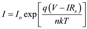
here I0 is the saturation current, feff is the zero bias barrier height, A** is the effective Richardson constant and is equal to 9.4 Acm−2∙k−2 for n-type InP [1], A is the diode area, n is an ideality factor, q is the charge electron, k is the Boltzmann’s constant and T is the absolute temperature. The saturation current I0 is determined by extrapolating the linear region of the forward-bias semi-log I-V curves to the zero applied voltage and the feff values are calculated from equation (2) and it can be written as
 (3)
(3)
Figure 1 shows the typical current-voltage (I-V) characteristics of Ni/Cu Schottky contacts to n-type InP before and after annealing temperature at 400˚C. It is noted that the leakage current of the as-deposited Ni/Cu Schottky contact is 9.09 × 10⁻⁵ A at −1 V. For the contacts annealed at temperatures 100˚C, 200˚C, 300˚C and 400˚C, the corresponding leakage currents are 1.54 × 10⁻⁴ A, 4.67 × 10⁻⁵ A, 2.40 × 10⁻⁵ A and 3.0 × 10⁻⁴ A at −1 V, respectively. It is observed that the leakage current decreases for the contact annealed at 300˚C compared to the as-deposited contact. However, it is observed that the leakage current slightly increases upon annealing temperature at 400˚C. Calculations showed that the Schottky barrier height (SBH) is 0.59 eV for the as-deposited contact. For the contacts annealed at 100˚C, 200˚C, 300˚C and 400˚C, the SBH are 0.56 eV, 0.62 eV, 0.65 eV and 0.54 eV. Based on the above observations, it is observed that the maximum barrier height is 0.65 eV for the contact annealed at 300˚C. Hence, the optimum temperature for the Ni/Cu Schottky contact is 300˚C.
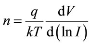
The ideality factor n is a measure of conformity of the diode to pure thermionic emission and if n is equal to one, pure thermionic emission occur, However, n has usually a value greater than unity. The values of n are determined from the slope of the linear region of the forward bias I-V characteristics using the relation [16].
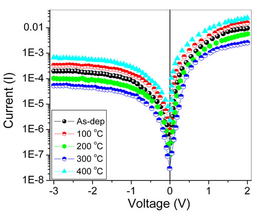
Figure 1. The reverse and forward bias current-voltage (I-V) characteristics of the Ni/Cu Schottky contact on n-type InP as a function of annealing temperature.
 (4)
(4)
The calculated ideality factor of Ni/Cu Schottky contact is found to be 1.32 for the as-deposited. For the contacts annealed at 100˚C, 200˚C, 300˚C, and 400˚C the ideality factors are 1.39, 1.20, 1.15 and 1.46, respectively. The values of ideality factors are indicative of non-ideal behavior, suggesting the transport mechanism, other than just thermionic are probably present in these diodes. Our data clearly shows that the diodes have ideality factors that are larger than one. The higher values of ideality factor are probably due to the potential drop in the interface layer and the presence of excess current and the recombination current through the interfacial states between the semiconductor/insulator layers [17]. The other reason for higher values of ideality factor “n” could be attributed to the inhomogeneous barrier height. Another possibility may be attributed to the oxide layer grown on the semiconductor, suggesting that the potential barriers at real metal-semiconductor interfaces depends much more the applied voltage than predicted ideal contacts.
The device shows a non-ideal current-voltage behavior due to the ideality factor being higher than unity. This may be due to the effect of series resistance and the presence of an interfacial layer. The series resistance (Rs) as well as other Schottky diode parameters such as ideality factor (n) and barrier height is also determined using the Cheung’s functions [18]. According to Cheung, the forward bias I-V characteristics due to the TE of a Schottky diode with the series resistance can be expressed as
 (5)
(5)
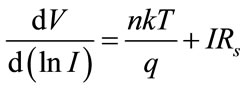
where the IRS term is the voltage drop across the diode due to series resistance. The values of the series resistance can be determined from following functions using equation (5)
 (6)
(6)
 (7)
(7)
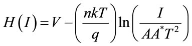
and H(I) is given as follows:
 (8)
(8)
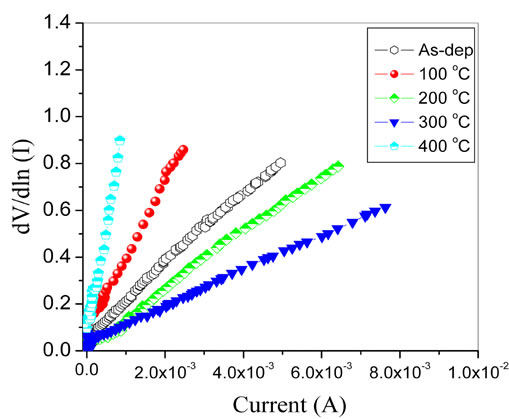
A plot of dV/dln (I) versus I will be linear and gives RS as the slope and nkT/q as the y-axis intercept from equation (6). Figure 2(a) shows a plot of dV/dln (I) versus I for Ni/Cu/n-InP Schottky contacts annealed at 100˚C, 200˚C, 300˚C and 400˚C respectively. The determined values of n and RS are 1.32 and 161 W for as-deposited, 1.15 and 75 W for 300˚C, and 1.46 and 874 W 400˚C respectively. It is observed that the value of ideality factor obtained from the forward bias ln(I)-V plot is agreeing with that of the dV/dn(I) versus I curves. A plot (Figure 2(b)) of H(I) versus I according to equation (8) will also give a straight line with y-axis intercept equal to nfbo. The estimated BH values are 0.59 eV, 0.56 eV, 0.62 eV, 0.65 eV and 0.54 eV for as-deposited, 100˚C, 200˚C, 300˚C and 400˚C respectively. The slope of this plot also provides a second determination of RS with the values of 150 W, 62 W and 609 W for the as-deposited, annealed at 300˚C and 400˚C respectively. It can be seen clearly that the values of fbo obtained from H(I) versus I curves are in close agreement with the values obtained from the ln (I)-V plot.
Since high series resistance can hinder accurate evolution of barrier height from the standard ln(I)-V plot [19], the Norde method is also employed to compare the Schottky barrier height of Ni/Cu/n-InP contacts. In this method, a function F(V) is plotted against voltage. The function F(V) is given by
 (9)
(9)
 (a)
(a)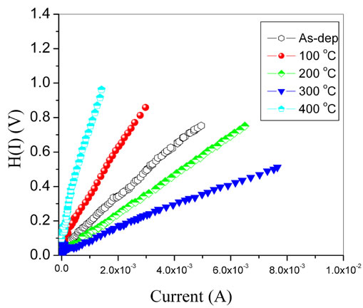 (b)
(b)
Figure 2. (a) dV/dlnI versus I, and (b) H(I) versus I plots of Ni/Cu/n-InP Schottky diodes.
The effective Schottky barrier height is given by
 (10)
(10)
where F(Vmin) is the minimum value of F(V) and Vmin is the corresponding voltage. A plot of F(V) versus V for the as-deposited and annealed samples at different annealing temperatures is shown in figure 3. Measurements showed that the SBHs are 0.62 eV for the as-deposited, 0.72 eV for 300˚C and 0.57 eV for 400˚C annealing contacts. These values are in good agreements with those obtained by the ln(I)-V method. Table 1 shows the values of SBHs (I-V and Norde), reverse leakage current, ideality factor and series resistance (dV/dln(I) versus I and H(I) versus I for as-deposited and annealed Ni/Cu Schottky contacts.
The annealing temperature treatment also has a large effect on diode I-V characteristics. Figure 4 shows a comparison of measured barrier height and ideality factor values for Ni/Cu/n-InP diodes annealed at 100˚C, 200˚C, 300˚C and 400˚C for 1 min in nitrogen ambient. Clearly indicate that the 300˚C annealing contact gives the best result (fb = 0.65 eV, n = 1.15) and also has the lowest reverse leakage current (2.40 × 10⁻⁵ A). However, the contact annealed at 400˚C, the barrier height significantly
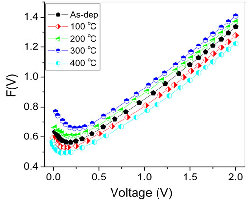
Figure 3. Plot of F(V) against V for Ni/Cu Schottky contacts annealed at different temperatures.
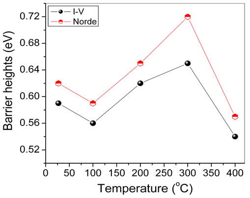
Figure 4. Plot of barrier heights against annealing temperatures for the Ni/Cu Schottky contacts on n-type InP.
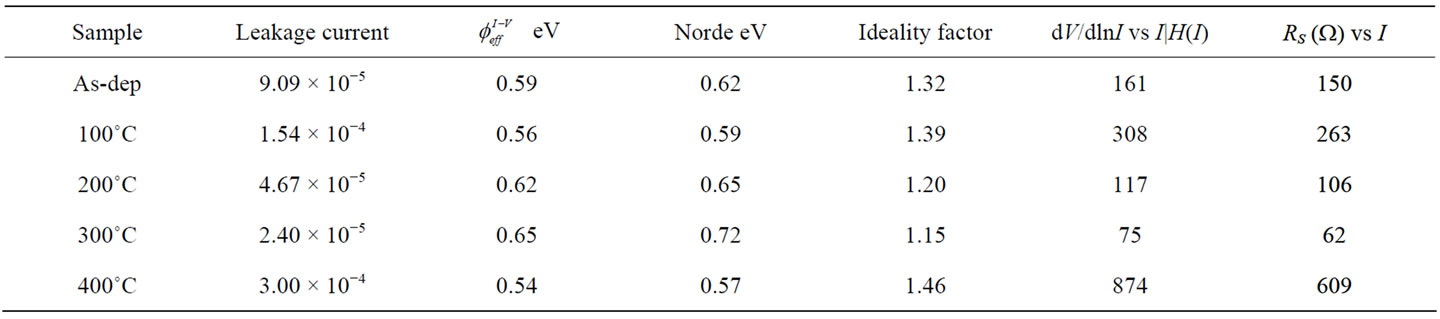
Table 1. The leakage current, Schottky barrier heights (fb), ideality factor (n) and series resistance (Rs) of Ni/Cu Schottky structure on n-InP as a function of annealing temperature.
decreased to 0.54 eV and the ideality factor (1.46) also deteriorated.
3.2. Structural and Morphological Characteristics
To identify the interfacial products that are formed at the interface before and after annealing at 400˚C, X-ray diffraction (XRD) measurement is used. Figure 5 shows the XRD plots of the Ni/Cu/n-InP Schottky diodes. For the as-deposited sample, figure 5(a), in addition to the characteristic peaks of InP (200) (400), there are other peaks observed, which are identified as Cu9In4 (200), Cu11In9 (400) and Ni12P5 (510). Figure 5(b) shows the XRD plot of the contact annealed at 300˚C. There are additional peaks are observed compared to the as-deposited contact, which indicate the formation of new interfacial phases. These phases are identified as Cu11In9 (111), Cu9In4 (200), In3Ni2 (101), In27Ni10 (420) and Ni12P2 (510). When the contact is annealed at 400˚C, figure 5(c), there are extra peaks in addition to the peaks observed in the 300˚C annealed contact. These peaks are identified as Cu3P (002), In12P5 (002) and Ni5P4 (210). The peaks corresponding to Cu11In9 (111), Cu9In4 (200), In3Ni2 (101) and In27Ni10 (420) had disappeared in the 400˚C annealed contact, which are observed in the 300˚C annealed contacts.
In order to characterize the changes of the surface morphology of Ni/Cu Schottky contacts as a function of annealing temperature, scanning electron microscopy (SEM) is employed. Figure 6 shows the plane-view SEM images obtain from the Ni/Cu/n-InP contacts before and after annealing at 400˚C. As can be seen from figure 6(a), the surface of the as-deposited contact is reasonably smooth. However, for the contact annealed at 300˚C, the surface of the contacts is slightly improve as shown in figure 6(b). Further, increase in annealing temperature up to 400˚C, the surface is slightly degraded as compared with that of the contacts annealed at 300˚C as shown in figure 6(c).
As generally known, the interface states and chemical reactions between the metals and semiconductor interfaces play an important role in determine the electrical behavior of devices. The degree of intermixing of In and P with the contact metal and the formation of surface states at the interface are influenced by the chemical reactivity of the metal with InP. The electrical measurements showed that the barrier height is increased for the
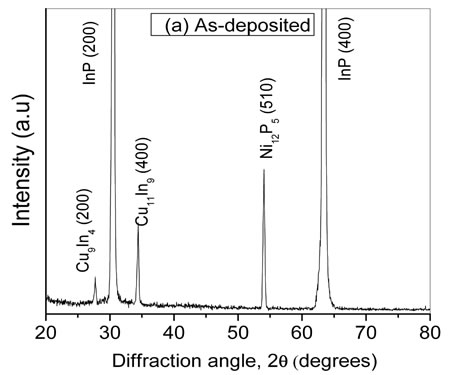
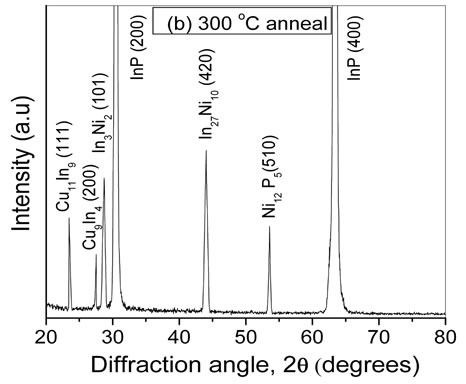
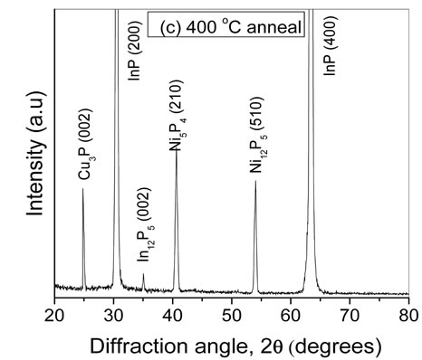
Figure 5. The XRD plot of the Ni/Cu Schottky contacts on n-type InP: (a) As-deposited (b) Annealed at 300˚C and (c) Annealed at 400˚C.
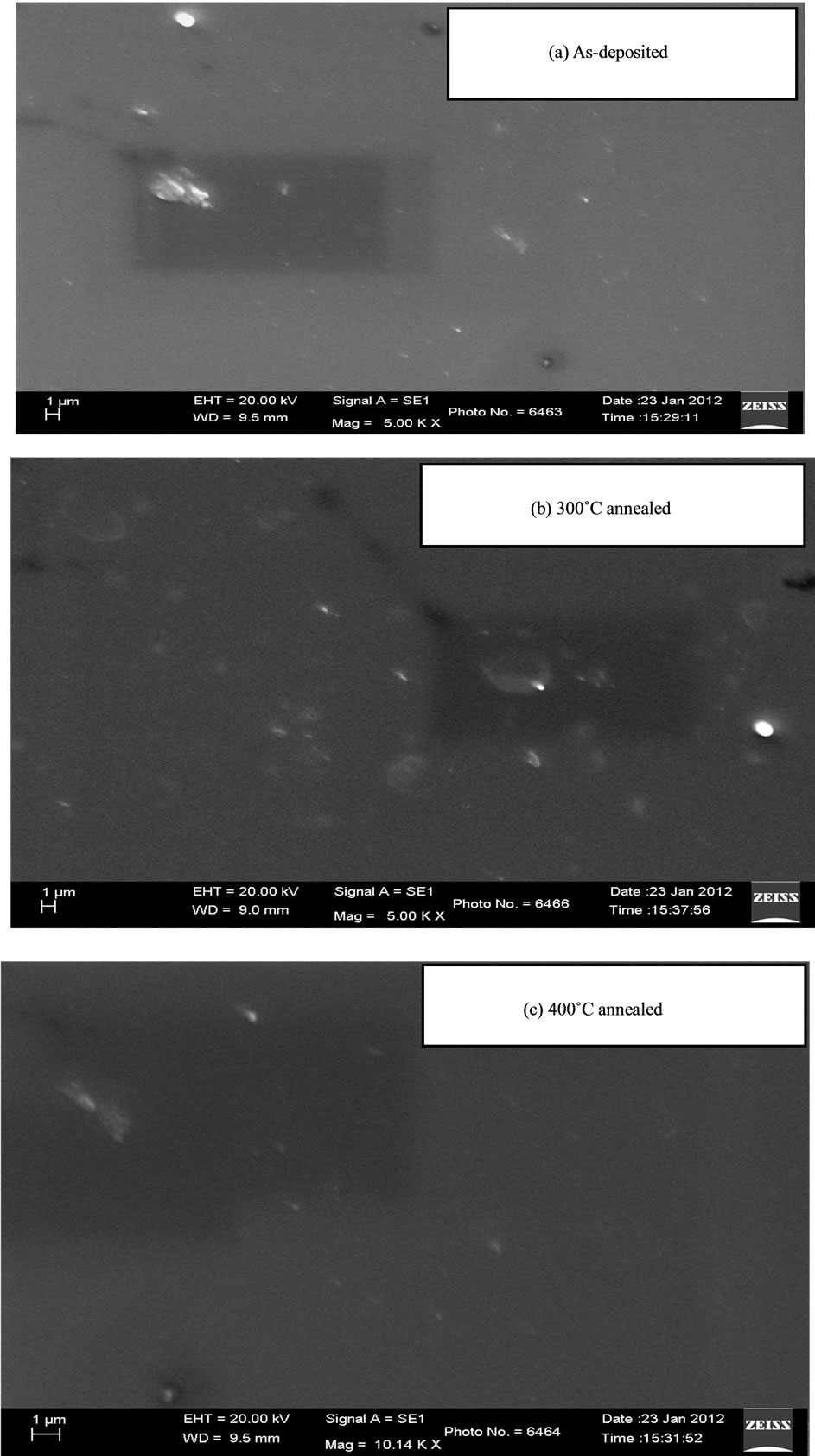
Figure 6. Scanning electron microscopy (SEM) micrographs of the Ni/Cu/n-InP Schottky diodes: (a) As-deposited (b) Annealed at 300˚C and (c) Annealed at 400˚C.
contact annealed at 300˚C compared to the as-deposited and annealed at 400˚C. The improved Schottky barrier height of Ni/Cu contact upon annealing at 300˚C could be ascribed to the interfacial reaction occurring between metal layers and InP. Based on the XRD results, the change in barrier height of the Ni/Cu Schottky contact with annealing temperature could be explained. The formation of Cu11In9 (111), Cu9In4 (200), In3Ni2 (101)In27Ni10 (420) and InNi2 (201) (as shown by XRD results in figure 5(b)), results in leads to the accumulation of indium vacancies at the InP surface region. This induces an increase in Schottky barrier height of the Ni/Cu contact which is extracted from I-V characteristics for the annealed contact at 300˚C. Another possibility is that a reduction of non-stoichiometric defects in the metallurgical interface [20] may also be the reason for the increase of Schottky barrier height. The decrease in barrier height after annealing at 400˚C may be due to the phase segregation of indium at the interface allowing relatively easy reactions between metal layers and InP which results in the formation of metal-anion complexes at higher temperatures [21]. At the 400˚C annealing temperature, the preferential out-diffusion of phosphorus leads to a loss of P from the surface. Loss P from the surface may lead to change in the interface state density distribution. In this case a positive charge states may exists at the interface due to loss of phosphorus from the surface. This may reduce the barrier height in the 400˚C annealed contacts than compared to the 300˚C annealed contact. This finding is consistent with the results previously reported by Andersson [22] and Ivey et al. [23]. They noted that the possible explanation for the disappearance of P from the near surface region after heat treatment the samples at high temperatures. This may be due to the loss of volatile P to the atmosphere. Reddy et al. [24] have explained the barrier height would be influenced by interfacial products in metal/GaN Schottky barrier diode. According to Duboz et al. [25] the lower value of the barrier height for sample annealed at higher temperature can be attributed to reduction in the density of interfacial defects. The modification of the defects density by annealing could change the pinning at the Fermi level what could resulted in change of the barrier height. Van de Walle et al. [26] have also explained the barrier height change for annealed metal/n-GaAs Schottky barrier diodes by the relation between the equilibrium interface charge and barrier heights. The variation of SBHs of Ni/Cu Schottky contact may be due to the observed structural changes in the Ni/Cu contacts on the surface.
4. Conclusion
In conclusion, we have investigated the effects of annealing temperature on electrical, interfacial reactions and surface morphological properties of Ni/Cu Schottky contacts by current-voltage (I-V), X-ray diffraction (XRD) and Scanning electron microscopy (SEM) measurements. The calculated Schottky barrier height of the as-deposited contact is found to be 0.59 eV (I-V) with an ideality factor of 1.32. However, it is observed that the barrier height slightly increases after annealing at 200˚C and 300˚C. Based on the experimental results, the highquality Schottky contact with barrier height and ideality factor of 0.65 eV (I-V) and 1.15 respectively, can be achieved after annealing at 300˚C for 1 min in a nitrogen atmosphere. However, it is noted that the Schottky barrier heights (SBHs) decreases for the contact annealed at 400˚C as compared to the as-deposited, 100˚C, 200˚C and 300˚C annealed samples. The Norde method is also employed to extract the barrier height of Ni/Cu Schottky contact, and the values are 0.62 eV for the as-deposited, 0.72 eV and 0.57 eV for the contact annealed at 300˚C and 400˚C respectively. These values are in good agreement with those obtained by I-V technique. From the above observations, it is noted that Ni/Cu Schottky contact exhibited excellent electrical properties after annealing at 300˚C. This indicates that the optimum annealing temperature for the Ni/Cu Schottky contact is 300˚C. Based on the results of XRD, it is concluded that the formation of indium phases at the Ni/Cu/n-InP interface may be the reason for the increase in the barrier height for the 300˚C annealed contact. The decrease in the barrier height upon annealing at 400˚C may be due to the formation of phosphide phases at the interface. Scanning electron microscopy (SEM) results show that the overall surface morphology of the Ni/Cu Schottky contact is reasonably smooth. From the above observations, the Ni/Cu Schottky contact is a good choice for the development of InP-based electronic device applications.
REFERENCES
- C. W. Wilmsen, “Physics and Chemistry of III-V Compound Semiconductor Interfaces,” Plenum Press, New York, 1985.
- R. T. Tung, “Recent Advances in Schottky Barrier Concepts,” Material Science Engineering R, Vol. 35, No. 1-3, 2001, pp. 1-138. doi:10.1016/S0927-796X(01)00037-7
- D. L. Lile and D. A. Collins, “An Insulated-Gate Charge Transfer Device on InP,” Applied Physics Letters, Vol. 37, No. 6, 1980, pp. 552-553. doi:10.1063/1.91983
- L. J. Brillson and C. F. Brucker, “Fermi-Level Pinning and Chemical Structure of InP Metal Interface,” Journal of Vacuum Science and Technology, Vol. 21, No. 2, 1982, pp. 564-569. doi:10.1116/1.571764
- S. Uno, T. Hashizume, S. Kasai, N.-J. Wu and H. Hasegawa, “0.86 eV Platinum Schottky Barrier on Indium Phosphide by in-Situ Electrochemical Process and Its Application to MESFETs,” Japanese Journal of Physics, Vol. 35, 1996, pp. 1258-1263. doi:10.1143/JJAP.35.1258
- H.-I. Chen and Y.-I. Chou, “A Comparative Study of Hydrogen Sensing Performances between Electroless Plated and Thermal Evaporated Pd/InP Schottky Diodes,” Semiconductor Science and Technology, Vol. 18, No. 2, 2003, pp. 104-110. doi:10.1088/0268-1242/18/2/307
- W.-C. Huang and D.-R. Cai, “Formation and Characterization of Aluminum-Oxide by Stack-Layered Metal Structure Schottky Diode,” International Workshop on Junction Technology, 2006, pp. 295-298.
- H. Cetin and E. Ayyildiz, “Electrical Characteristics of Au, Al, Cu/n-InP Schottky Contacts Formed on Chemically Cleaned and Air-Exposed n-InP Surface,” Physica B: Condensed Matter, Vol. 394, No. 1, 2007, pp. 93-99. doi:10.1016/j.physb.2007.02.013
- O. Gullu, “Ultrahigh (100%) Barrier Modification of n-InP Schottky Diode by DNA Biopolymer Nanofilms,” Microelectronic Engineering, Vol. 87, No. 4, 2010, pp. 648-651. doi:10.1016/j.mee.2009.09.001
- N. Ucar, A. F. Ozdemir, D. A. Aldemir, S. Cakmak, A. Calik, H. Yildiz and F. Cimilli, “The Effect of Hydrostatic Pressure on the Electrical Characterization of Au/nInP Schottky Diodes,” Superlattices and Microstructures, Vol. 47, No. 5, 2010, pp. 586-591. doi:10.1016/j.spmi.2010.02.003
- M. Bhaskar Reddy, V. Janardhanam, A. Ashok Kumar, V. Rajagopal Reddy and P. Narasimha Reddy, “Influence of Rapid Thermal Annealing on Electrical and Structural Properties of Double Metal Structure Au/Ni/n-InP (111) Diodes,” Current Applied Physics, Vol. 10, No. 2, 2010, pp. 687-692. doi:10.1016/j.cap.2009.09.001
- S. Sankar Naik, V. Rajagopal Reddy, C.-J. Choi and J.-S. Bae, “Electrical and Structural Properties of Double Metal Structure Ni/V Schottky Contacts on n-InP after Rapid Thermal Process,” Journal of Material Science, Vol. 46, No. 2, 2011, pp. 558-565. doi:10.1007/s10853-010-5020-4
- A. Ashok Kumar, V. Janardhanam and V. Rajagopal Reddy, “Electrical, Structural and Morphological Characteristics of Rapidly Annealed Pd/n-InP (100) Schottky Structure,” Journal of Martial Science: Material Electronics, Vol. 22, No. 7, 2011, pp. 854-861. doi:10.1007/s10854-010-0225-5
- S. Sankar Naik, V. Rajagopal Reddy, C.-J. Choi and J.-S. Bae, “Electrical and Structural Properties of Pd/V/n-Type InP Schottky Structure as a Function of Annealing Temperature,” Surface and Interface Analysis, Vol. 44, No. 1, 2012, pp. 98-104. doi:10.1002/sia.3778
- G. Myburg and F. D. Auret, “Influence of the Electron Beam Evaporation Rate of Pt and the Semiconductor Carrier Density of the Characteristics Pt/n-GaAs Schottky Contacts,” Journal of Applied Physics, Vol. 71, No. 12, 1992, pp. 6172-6176. doi:10.1063/1.350426
- E. H. Rhoderick and R. H. Williams, “Metal-Semiconductor Contacts,” 2nd Edition, Clarendon, Oxford, 1988.
- D. T. Quan and H. Hbib, “High Barrier Height Au/n-Type InP Schottky Contacts with a POxNyHz Interfacial Layer,” Solid State Electronics, Vol. 36, No. 3, 1993, pp. 339-344. doi:10.1016/0038-1101(93)90085-5
- S. K. Cheung and N. W. Cheung, “Extraction of Schottky Diode Parameters from Forward Current-Voltage Characteristics,” Applied Physics Letters, Vol. 49, No. 2, 1986, pp. 85-87. doi:10.1063/1.97359
- H. Norde, “A Modified Forward I-V Plot for Schottky Diodes with High Series Resistance,” Journal of Applied Physics, Vol. 50, No. 7, 1979, pp. 5052-5053. doi:10.1063/1.325607
- W. E. Spicer, I. Lindau, P. Skeath, C. Y. Su and P. Chye, “Unified Mechanism for Schottky-Barrier Formation and III-V Oxide Interface States,” Physical Review Letters, Vol. 44, No. 6, 1980, pp. 420-423. doi:10.1103/PhysRevLett.44.420
- T. S. Huang and R. S. Fang, “Barrier Height Enhancement of Pt/n-InP Schottky Diodes by P2S5/(NH4)2S Solution Treatment of the InP Surface,” Solid State Electronics, Vol. 37, No. 8, 1994, pp. 1461-1466. doi:10.1016/0038-1101(94)90152-X
- M. Andersson, “Ternary Phase Equilibria in the (Cr, Mo, W)-In-P Systems at 600˚C,” Journal of Alloys and Compound, Vol. 198, No. 1-2, 1993, pp. L15-L18. doi:10.1016/0925-8388(93)90134-9
- D. G. Ivey, P. Jian and R. Bruce, “Reactions between Pd Thin Films and InP,” Journal of Electronic Materials, Vol. 21, No. 8, 1992, pp. 831-839. doi:10.1007/BF02665523
- V. Rajagopal Reddy and P. Koteswara Rao, “Annealing Temperature Effect on Electrical and Structural Properties of Cu/Au Schottky Contacts to n-Type GaN,” Microelectronic Engineering, Vol. 85, No. 2, 2008, pp. 470-476. doi:10.1016/j.mee.2007.08.006
- J. Y. Duboz, F. Binet, N. Laurent, E. Rosencher, F. Scholz, V. Harle, O. Briot, B. Gil and R. L. Aulombard, “Influence of Surface Defects on the Characteristics of GaN Schottky Diodes,” Material Research Society Symposium Proceedings, Vol. 449, 1996, pp. 1085-1090. doi:10.1557/PROC-449-1085
- R. Van de Walle, R. L. Van Meirhaeghe, W. H. Laflere and F. Cardon, “On the Relationship between Interfacial Defects and Schottky Barrier Height in Ag, Au, and Al/nGaAs Contacts,” Journal of Applied Physics, Vol. 74, No. 3, 1993, pp. 1885-1889. doi:10.1063/1.354797
NOTES
*Corresponding author.