Journal of Modern Physics
Vol.3 No.6(2012), Article ID:20099,5 pages DOI:10.4236/jmp.2012.36063
Excitation Transfer in Vertically Stacked in (Ga)As/GaAs Quantum Rings
1Unité de Recherche des Physiques des Semiconducteurs et Capteurs, Institut Préparatoire aux Etudes Scientifiques et Techniques, Université Carthage, Tunis, Tunisia
2Instituto de Ciencia de los Materials, Universidad de Valencia, Valencia, Spain
3Instituto de Microelectrónica de Madrid, Madrid, Spain
Email: *naouari_raja@hotmail.fr
Received November 30, 2011; revised January 5, 2012; accepted January 24, 2012
Keywords: Quantum rings; Vertical stack; Time resolved photoluminescence
ABSTRACT
Carrier tunnelling through GaAs barriers of different thicknesses is investigated in vertically InGaAs/GaAs quantum rings (QR’s). Shorter PL decay time of the ground state emission of high-energy component in the sample with thicker spacer (1.5 nm) is ascribed to both tunnelling effect between the two QR families and vertical coupling between layers in the stacks. We found that tunnelling time between QR’s followed the Wentzel-Kramers-Brillouin (WKB) approximation. The non resonant tunnelling rate between QR’s is found to be different by one order of magnitude from the rate in quantum dots (QD’s).
1. Introduction
Tunneling of carriers in semiconductor heterostructures has been intensively investigated because of its basic quantum mechanical aspect [1-3] and the importance for both physics and applied physic. In particular, time-resolved optical techniques revealed the dynamics of tunneling in double barriers [4], in asymmetric double quantum as well (ASDQW) [5] and in QD structures [2,3].
The tunnelling time between QD’s is known to follow the Wentzel-Kramers-Brillouin (WKB) approximation [2,3] and is governed by longitudinal optical (LO) phonon-assisted tunneling under non resonant tunneling conditions [6].
In QD, the estimation of PL decay time down to 20 ps has been attributed to carrier transfer between different layers of QD stacks separated by GaAs spacer layer, from the smaller QDs in the seed layer to the larger QD’s in the second layer [3].
In InAlAs QD’s, in the case of non resonant excitation the tunneling time is found to be one order of magnitude larger than that found in InAs QD’s. In the same paper, the tunnelling time is 130 ps for the vertically stacked In0.9Al0.1As with barrier thickness of 6 nm [2].
QRs are also important for 980 nm optoelectronic devises and commonly used to increase the active volume in the optical devices, which are of interest for applications in telecommunications. When QD are employed in the active region of laser devises, the use of stacked layer is necessary to avoid saturation gain effect. It has been shown [7] that the optical mod loss does not increase as the numbers of layers increase. Whereas the modal gain obtained from the dot ground state increases. When QRs are employed in active region, stacking of the nanostructures is more even more important due to the low density of ring ensembles (2 ´ 109 - 9 ´ 109 cm−3). The use of higher QR sheet densities could lead to overlap problems because of the large in-plane dimension of rings (100 nm ´ 90 nm).
PL and TRPL for In(Ga)As/GaAs QRs in such stacked samples show the energy transfer processes between layers and allows the estimation of the non resonant carrier tunnelling time in vertically aligned triple QR’s structures. The carrier transfer rate by tunnelling in a QR’s is found to be enhanced than that in double QD’s. The difference in the tunnelling rate between the QR’s and the QD’s is deduced.
In this paper, we present a detailed study of the carrier transfer between two QR families with different slight average size distribution, but separated by a thin GaAs spacer layer. The particular QR under investigation is a vertically aligned triple—layers In(Ga)As/GaAs QR structure. It is interesting to study such heterostructures because of the difference in the spatial distribution of wave functions envelops and the difference in the vertical carrier confinement compared to the QDs.
2. Samples and Experiment
2.1. Preparation
The samples under study have been grown with three layers of QR, grown by molecular beam epitaxy (MBE). Each sample with different spacer between layers: 1.5, 2 and 4.5 nm. In each layer, the total amount of deposited InAs was just above the critical thickness (1.6 ML) necessary for the 3D transition to take place (checked with RHEED). The QRs were obtained after a growth interruption when the dots were partially covered with 2 nm of GaAs under un As2 flux, because of the balance between material intermixing [8]. More details about the growth of these samples can be found in reference [9].
2.2. Characterization (PL Experiments)
The continuous wave PL experiments were performed by using the 514 nm Ar+ line as excitation source. The PL signal was dispersed by monochromator and synchronously detected with a cooled Ge detector. In time resolved experiments, sample excitation at 750 nm was done by a green-ND:YVO4 (Verdi, coherent) pumped mode locked Ti:Saphire laser (Mira 900D, coherent), providing 2 ps pulses at a repetition rate of 76 MHz. The PL signal was dispersed by a single 0.5 m focal length imaging spectrograph and detected by a synchroscan streak camera (Hamamatsu C5680) with a type S1 cooled photocathode. The overall time response of the system in the widest temporal window (about 2 ns) was around 40 ps (full width at half maximum). In both kinds of experiments, the samples were held in the cold finger of a closed-cycle cryostat to vary the temperature in the range 12 - 300 K, approximately.
3. Experimental Results
Figure 1 shows the low excitation density PL spectra, which is mainly dominated by exciton recombination of the ground states of the QR ensembles. This ensures that we only observe emission from the optically active ground state of quantum rings. The emission peaks from the samples with GaAs barriers of 1.5, 2 and 4.5 nm were at energies of 1.328, 1.356 and 1.371 eV, respectively. However, their PL spectra is not a perfect Gaussian, but rather asymmetric. This can be to the total contribution in the PL signal from the QR ensembles of the three layers stacked. Indeed a line shape analysis shows that the PL signal of the sample can be reproduced by two Gaussian peaks, as shown in Figure 1. We attribute the measured PL band to a bi-modal size distribution of the QR en
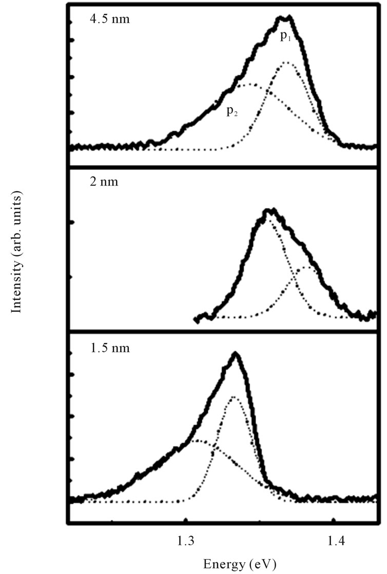
Figure 1. TIF: Photoluminescence (continuous line) spectres for samples with various spacer widths at 10 K. The excitation density is about 3 W/cm2.
semble (i.e., two different size families), being similar in each of the three stacked layers, in average. For the 1.5 nm spacer, the spectra are red shift with respect to the emission of sample with 4.5 nm spacer. This phenomenon can be attributed to the vertical electronic coupling between layers as it has been observed and calculated in InAs/GaAs quantum dot system [10].
Figure 2 shows the PL transients measured at 10 K for the detection energy corresponding to high-energy peak (P1). In the measurement condition, all the measured PL curves exhibit mono exponential decay. This suggests that the PL arises from the ground state of the QR’s. The high Gaussian components decay times obtained from monoexponential fitting are plotted in Figure 3 as a function of the spacer thickness.
Figure 3 shows the spacer width dependence of the decay time, plotted as a function of the detection energy for the three samples.
The decrease of the decay time in the high energy peak with decreasing the spacer thickness has been studied in details in reference [11]. When using an extremely narrow GaAs spacer, i.e. the case of sample with 1.5 nm spacer,
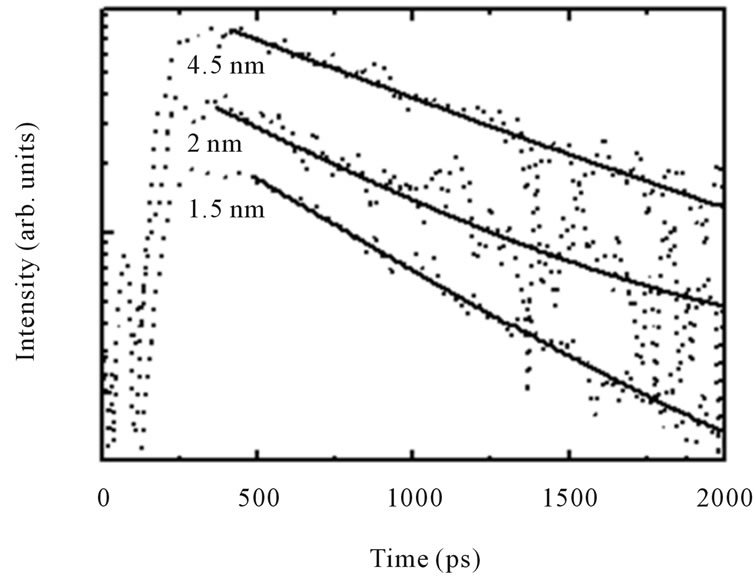
Figure 2. TIF: Photoluminescence transients at 10 K for the component P1 measured under low excitation density (4 W/cm2) for different spacer width and the corresponding mono-exponential fit.
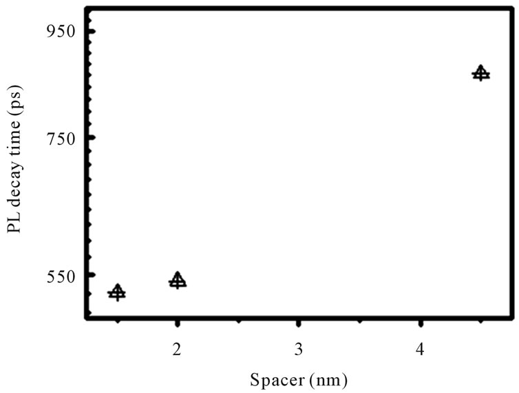
Figure 3. TIF: Decay time of the high-energy peak (p1) as a function of the spacer width.
the electronic coupling is so important. It is interesting to note that the average height of uncovered rings is around 1.5 nm, that is, very close to the used spacer thickness. In this case, the probability of non-resonant exciton tunnelling is greater than that in sample with spacer higher than 1.5 nm, because the S-exciton at P1-QR can tunnel towards (near) P-states at P2-QR in every of the three layers.
Figure 4 shows the spacer width dependence of the decay time, plotted as a function of the detection energy for the three samples. The time decay is constant for the broad size distribution of nanostructures and decrease from low to high PL detection energy. The detection energy has notable effect on the dependence of the decay lifetime, which decreases for higher detection energies (above P1 peak).
In previous work for GaAs based InAs QDs reported
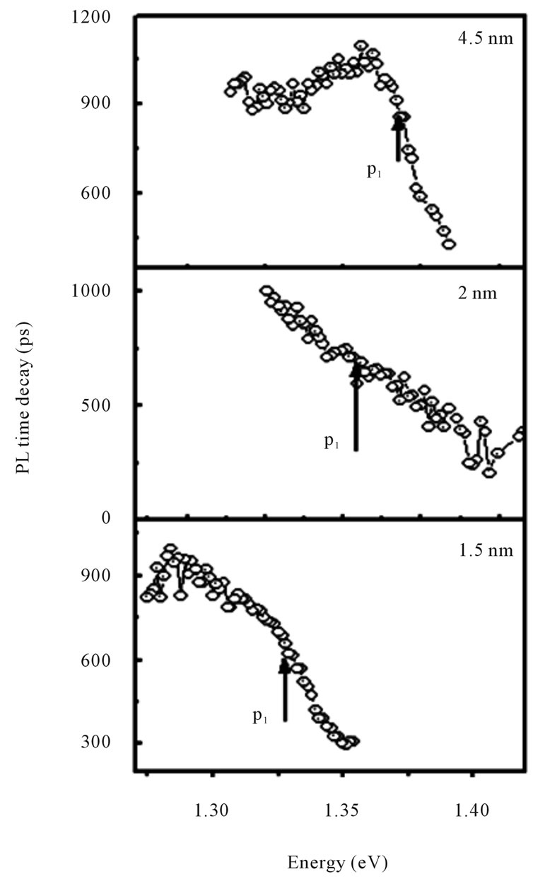
Figure 4. TIF: Decay time as a function of the detection energy for different spacer width.
by sanguinetti et al., the carriers dynamic and the radiative efficiency of the QDs were negatively affected by reducing the GaAs spacer thickness [12]. That is, with a decrease in the spacer thickness, the defect caused by the relaxation of accumulated large strain was significantly considered. The activation energy deduced from non radiative time at high temperature with TRPL measurement in the three sample are very close and range between 37 and 40 meV. The effect of defect generation in time decay thus can be excluded for our samples.
In reference 2, tunnelling between vertically stacked In0.9Al0.1As QD was discussed. For vertical tunnelling with well defined barrier high of 140 meV and barrier thickness of 6, 8 and 10 nm, a good agreement between the measured tunnelling times of 130, 370 and 850 ps and semi classical WKB description has been found.
In the present samples structures, with the barrier thickness of 1.5 nm, the non resonant time is estimated at T = 10 K to be 1580 ps. In sample with 4.5 nm spacer, the estimated  is 6070 ps. The large value of
  in comparison with the ground state lifetime is in good agreement with the result in reference [3]. We evaluated the tunnelling time between the two QR families (P1 to P2) from the observed decay times using the following equation:
Here  is the tunnelling time from the upper ring (P1) to the lower ring (P2).
The tunnelling time of the QR’s are actually one order of magnitude longer than those of QD found in the reference [2].
Now, we try to discuss of the underlying tunnel mechanisms. At low temperature, the calculated difference E(p1)-E(p2) is respectively 23, 24 and 32 meV in samples 1.5, 2 and 4.5 nm spacer. We note that ΔE is significantly lower than in InGaAs/GaAs 2D QW’s case where  corresponds to the optical-phonon energy (36 meV) in GaAs [13]. This result is in agreement with the situation of strong electron-LO-phonon interaction. In this case, the activation energy is not equal to ħwLO but it is equal to the energy separation between excited and ground levels of polaron [14]. Non resonant tunnelling by emission of optical phonon can be considered in our samples.
The non-resonant times depend exponentially on the barrier thickness  according to
V0 denotes the conduction-band barrier height, E and m* the confinement energy and electronic effective mass in the barrier.  is also plotted as a function of the quality
  in order to account for the different structures parameters in GaAs (Figure 5). After calculation [15,16], we expect Ve-Ee ~90 meV and Vh-Eh ~70 meV added to the high
  we expected tunneling of electrons. We calculated the experimental values Ve-Eground ~1/3 ´ (EGaAs-EPL).
At low temperature, two important points should make: first, the exponential slope α(0.2) following a low  , is the same order of magnitude as the one observed for non resonant tunneling in GaAs QDs [2]. The coincidence of the slopes implies that both carriers transfer mechanisms are governed by the same processes. On the other hand, the coefficient of proportionality
  (800 ps) is two orders of magnitude bigger than the one obtained in QDs.
The difference in the magnitude of the tunneling time and the coefficient  implies that the efficiency of the scattering that assists the non resonant tunnelling effect differs between QD’s and QR’s.
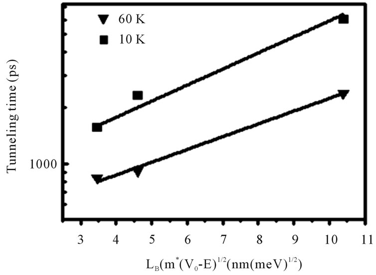
Figure 5. TIF: Tunnelling time the vertically aligned QRs for different temperature as a function of the effective barrier width on a logarithmic scale. The solid line is fitted to tunnelling time by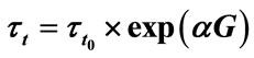 .
.
An enhanced exciton LO phonon coupling and the continuum states with small density of states [17] have been found in QD’s. Both effects enhance the measurement tunnelling time as compared from the tunnelling time found in QW’s.
In our case, the reduced transfer rate in QR’s At 10 K could be due to the difference in magnitude in the volume between QR and QD in the seed layer.
At high temperature (60 K), the exponential slope α(0.15) measured in this work is the close to the value found at low temperature and  (400 ps) is roughly half as small as the one observed at low temperature. This suggests that α does not depend on temperature.
At high temperature (60 K), the following mechanism can explain such behaviour: the volume of QR in the seed layer is smaller than a QD seed layer. Therefore, their optical confinement is also minor and this effect favours the transfer to the rings having a higher binding energy and then relaxes in the low energy rings in the seed layer (layer of P1 peak). The difference in energy becomes smaller than at 10 K, resulting in mixing of the wave functions and the tunnelling effect must be significantly higher.
Differences in carrier transfer at low excitation density between QR and QD are likely due to the difference in energy and the spacing of QR states in InGaAs/GaAs heterostructures at higher temperature but this effect is ineffective for the carrier transfer at low temperature.
A quantitative analysis of such mechanisms requires a fully quantum-mechanical description taking into account The QR’s size as well as the barrier width in such system.
The low optical confinement in QR, reduces the possibility of achieving a working laser devises at room temperature with three stacked layers of rings. To overcome this limitation we have to increase the number of stacked layers more than three.
4. Conclusions
In Summary, the tunnelling processes in In(Ga)As/GaAs QRs are investigated by PL time resolved. The dependence on the tunnelling times on the barrier thickness is in good agreement with the behaviour observed in QD’s. We found that tunnelling time between QR’s follows the Wentzel-Kramers-Brillouin (WKB) approximation.
The non resonant tunneling time between QR’s is found to be different by one order of magnitude from the time in QD’s. This different value is due to the difference in the volume of QR in the seed layer compared to the QD’s. At high temperature, the tunneling effect is becoming significantly higher.
We have uncovered a more complete picture of carrier transfer in multimodal QR systems, which will provide measures for greater control PL behaviours.
REFERENCES
- S. Luryi, “Possibility of a Direct Observation of the Time Evolution in Heterostructure Barrier Tunnelling,” Solid State Communications, Vol. 65, No. 8, 1988, pp. 787-789. doi:10.1016/0038-1098(88)90505-4
- A. Takeuchi, T. Kuroda, K. Mase, Y. Nakata and N. Yokoyama, “Dynamics of Carrier Tunneling between Vertically Aligned Double Quantum Dots,” Physical Review B, Vol. 62, No. 3, 2000, pp. 1568-1571. doi:10.1103/PhysRevB.62.1568
- R. Heitz, I. Mukhametzov, P. Chen and A. Madhukar, “Quantitative Study of C-H Bonding in Polymerlike Amorphous Carbon Films Using in Situ Infrared Ellipsometry,” Physical Review B, Vol. 58, No. 20, 1998, pp. 13957- 13973. doi:10.1103/PhysRevB.58.13957
- M. Tsuchiya, T. Matsusue and H. SaKaki, “Tunneling Escape Rate of Electrons from Quantum Well in DoubleBarrier Heterostructures,” Physical Review Letters, Vol. 59, No. 20, 1987, pp. 2356-2359. doi:10.1103/PhysRevLett.59.2356
- B. Deveaud, et al., “Tunnelling and Relaxation in Coupled Quantum Wells,” Europhysics Letters, Vol. 11, No. 4, 1990, p. 367. doi:10.1209/0295-5075/11/4/013
- S. Moto, T. Inata, A. Takeuchi, Y. Sugiyama and T. Fujii, “Longitudinal-Optical-Phonon Assisted Tunneling in Tunneling bi-Quantum Well Structures,” Applied Physics Letters, Vol. 58, No. 21, 1991, p. 2393. doi:10.1063/1.104881
- P. M. Smowton, E. Hermann, Y. Ning, H. D. Summers and P. Blood, “Optical Mode Loss and Gain of MultipleLayer Quantum-Dot Lasers,” Applied Physics Letters, Vol. 78, No. 18, 2001, p. 2629. doi:10.1063/1.1366652
- M. L. Dotor, Recio, D. Golmayo and F. Briones, “Photoluminescence Caracterisation of GaAs Quantum Well Laser Structure with AlAs/GaAs Superlatices Waveguide,” Journal of Applied Physics, Vol. 72, No. 12, 1992, pp. 5861-5866.
- F. Suarez, D. Gradanos, M. L. Dotor and J. M. Garcia, “Laser Devices with Stacked Layers of InGaAs/GaAs Quantum Rings,” Nanothechnology, Vol. 15, No. 4, 2004, pp. 126-130.
- P. Miska, J. Even, C. Paranthoen, O. Dehaese, A. Jbeli, M. Senes and X. Marie, “Vertical Electronic Coupling between InAs/InP Quantum-Dot Layers Emitting in the Near-Infrared Range,” Applied Physics Letters, Vol. 86, No. 11, 2005, pp. 111905-111907. doi:10.1063/1.1865332
- W. Ouerghui, J. Martinez-Pastor, J. Gomis, M. A. Maaref, D. Granados and J. M. Garcia, “Lateral Carrier Tunnelling in Stacked In(Ga)As/GaAs Quantum Rings,” The European Physical Journal B, Vol. 54, No. 2, 2006, pp. 217-223. doi:10.1140/epjb/e2006-00444-x
- S. Sanguinetti, M. Padovani, M. Guirioli, E. Grilli, M. Guzzi, A. Vinattieri, M. Collocci, P. Frigeri, S. Franchi, L. Lazzarini and G. Salviati, “Study of GaAs Spacer Layers in InAs/GaAs Vertically Aligned Quantum Dot Structures,” Thin Solid Films, Vol. 380, No. 1-2, 2000, pp. 224- 226. doi:10.1016/S0040-6090(00)01511-X
- P. Borri, et al., “Well-Width Dependence of ExcitonPhonon Scattering in InxGa1-xAs/GaAs Single Quantum Wells,” Physical Review B, Vol. 59, No. 3, 1999, pp. 2215-2222. doi:10.1103/PhysRevB.59.2215
- O. Verzelen, R. Ferreira and G. Bastard, “Excitonic Polarons in Semiconductor Quantum Dots,” Physical Review Letters, Vol. 88, No. 14, 2002, pp. 146803-146806. doi:10.1103/PhysRevLett.88.146803
- S.-S. Li and J.-B. Xia, “Valence Band Structures of the InAs/GaAs Quantum Ring,” Journal of Applied Physics, Vol. 91, No. 5, 2001, pp. 3227-3231. doi:10.1063/1.1446240
- S.-S. Li and J.-B. Xia, “Electronic States of InAs/GaAs Quantum Ring,” Journal of Applied Physics, Vol. 89, No. 6, 2000, pp. 3434-3437. doi:10.1063/1.1347409
- Y. Toda, O. Moriwaki, M. Nishioka and Y. Arakawa, “Efficient Carrier Relaxation Mechanism in InGaAs/ GaAs Self-Assembled Quantum Dots Based on the Existence of Continuum States,” Physical Review Letters, Vol. 82, No. 20, 1999, pp. 4114-4117. doi:10.1103/PhysRevLett.82.4114
NOTES
*Corresponding author.