Journal of Modern Physics
Vol. 2 No. 10 (2011) , Article ID: 8050 , 16 pages DOI:10.4236/jmp.2011.210139
Materials for Spintronics: Magnetic and Transport Properties of Ultrathin (Monolayer Graphene)/MnO(001) and MnO(001) Films
Don State Technical University, Rostov-on-Don, Russia
E-mail: *viily@mail.ru
Received May 17, 2011; revised July 1, 2011; accepted July 17, 2011
Keywords: Magnetism, Electron Structure, Ultrathin Films, Graphene, Manganese Oxide, Spintronics
ABSTRACT
Results of investigations of band structure, Fermi surface and effective masses of charge carriers in the ultrathin (monolayer graphene)/MnO(001) and MnO(001) films are presented using the method of the density functional theory. Features of spin states of valence band and Fermi level as well as an interatomic interaction in these systems are discussed. A magnetic moment at Mn atom is estimated and an effect of spin polarization at atoms of oxygen and carbon has been revealed which natures are discussed. By calculations of structural energies for 2D (monolayer graphene)/MnO(001) and 2D MnO(001) a stability of these systems has been ascertained. In the 2D (monolayer graphene)/MnO(001) and 2D MnO(001) systems the band structure calculations for the 2D systems mentioned above point out that tensor components of effective masses of both electrons and holes are in the ranges of (0.15 - 0.54) m0 and (0.38 - 1.27) m0 respectively. Mobility estimations of two-dimensional charge carriers for a 2D (monolayer graphene)/MnO(001)AF2 heterostructure have been performed.
1. Introduction
One of the perspective directions in creation of devices for nanoand spintronics is concerned with use of recently discovered graphite-like allotropic modifications of carbon: graphene and graphene oxide which possess unique properties [1-3]. Since graphene was discovered it has been successfully synthesized on substrates with various surface crystal geometries [4-7]. However known synthesis methods permit to produce graphene of high quality under the laboratory conditions only [8] that limits their industrial application. A suggested method [9] of plasma deposition from vapor phase (PECVD) of high quality graphene sheets can play an important role for becoming of graphene nanoelectronics [6].
One of the simple solutions in creation of devices for spintronics can be use of graphene, i.e., of a heterointerface of the graphene/(ferromagnetic metal) type, instead of nonmagnetic semiconductor. Graphene is an ideal material for spintronics due to a small spin-orbital interaction as well as a vanishing nuclear magnetic moment of carbon atom. Recently an injection of spin polarized electrons and their registration in graphene at room temperature have been experimentally demonstrated [10-12]. The spin polarization of the injected electrons has amounted to about 10%. An increase in the part of the spin polarized injected electrons (up to ~90%) has turned out to be possible in a hybrid (Cd, Mn)Te/GaAs structure [13]. Similar structural elements are used as units of devices that produce flows of external electrons with the maximum polarization, for instance in quantum cascade lasers [14].
So the ferromagnetic heterointerface study and a combination of the most attractive magnetic and semiconductor materials in a hybrid structure are of a high scientific and practical interest. In the present paper it is emphasized a substitution for ferromagnetic metal in the hybrid graphene/(ferromagnetic metal) system by ferromagnetic metal oxide, i.e., the substitution for a Al2O3/Co interface in the system considered above [10] by MnO. This choice is caused by the fact that structures based on transition metals oxides attract a special attention due to their astonishing electronic and magnetic properties. In particular among oxides of transition 3d-metals MnO plays a special role due to a high-spin main state of 3d5-configuration of Mn2+ ion. Moreover manganese oxide in antiferromagnetic ordering has an electron energy structure with an energy gap value such as Eg > 1.0 eV [15] that is typical for magnetic semiconductors. Therefore MnO oxide can be an ideal model system to study both spin dependence and magnetic interaction of an electron subsystem in the graphene/ (ferromagnetic metal oxide (magnetic semiconductor)) ferromagnetic heterointerface.
Achievements in growing of ultrathin MnO, FeO, CoO, and NiO layers by means of an impulse laser deposition method [16,17] have permitted to produce high-quality magnetic heterostructures such as MnO/CoO/MnO/ Ag(001) [18]. An exchange interaction in multilayer magnetic systems opens a possibility in particular for the spin regulation [19-21]. By the methods of low energy electron diffraction (LEED) and X-ray photoelectron diffraction (XPD) features of growth of the ultrathin MnO layers obtained with the impulse laser deposition [17] have been studied. It has shown [22] that an atom structure of the ultrathin 2D MnO layers essentially depends on thickness of grown layer. On the basis of both X-ray methods of absorption spectroscopy (XAS) and photoelectronic one (XPS) it has shown that electron and crystalline properties of the 2D MnO/Ag(001) ultrathin film and 3D MnO crystal are different [23]. In the cohesive energy range of 7 - 12 eV the electron structure of the ultrathin MnO layers possibly contains contributions of much more quantity of vacancies than in 3D MnO [23]. As a result experimental X-ray absorption spectra as well as X-ray photoelectronic ones can contain some amount of artefacts which detailed theoretical analysis is necessary.
The electron structure and magnetic properties of the 3D MnO crystal have been completely enough investigated with band theory methods [15,24-26]. Results of calculations of magnetic moments at Mn atoms are in a good agreement with experimental data [23,27,28]. In one of the last papers [29] a correlation between the electron structure and the magnetic as well as optical properties of 3D MnO has been studied by means of four different band theory methods such as the local density approximation+Hubbard U (LDA+U), the pseudopotential self-interaction correction (pseudo-SIC), the local spin density SIC (SIC-LSD) method and the hybrid functional (combined local exchange plus Hartree-Fock exchange). By authors of the paper [29] it has been convincingly shown that use of the different band theory calculation methods permits to obtain consistent estimations of the magnetic moments for the high-spin  configuration of
  ion. On the basis of the considered methods a difference in a magnetic moment value amounts to ~0.3
 (without pressure). However use of the band theory methods [29] gives fundamental band gap
  estimations which are in the range of 2 - 4 eV. Such a scatter of the
  values is caused by capacities of the quoted band theory methods [29]. The crucial point is an exchange-correlation energy calculation that is determined by the approximation type (LDA+U, HSE, PBE and others) as well as a shape of potential. In a paper [30] we have shown that for the correct spin state simulation of magnetic materials a nonlocal exchange-correlation functional in the PBE96 form can be successfully used. There are experimental and theoretical papers [31-34] devoted to investigations of stability, structural and oscillatory properties of epitaxial MnO layers on various substrates. However as far as we know there are no papers devoted to the theoretical study of both electron structure features and transport properties in the interface of the ultrathin graphene/ MnO(001) layers.
Of particular interest is the magnetism of the monolayer graphene (MG). The investigation of the interface between graphene and underlayer can be the key to this magnetism understanding. The possibility of the chemical interaction between graphene and metals was noted in MG/Me (Me = Ni, Pt) systems [35-41]. On the basis of ab initio calculations authors of a paper [36] suppose that a formation of chemical bonds between some of carbon atoms of graphene and a SiC(0001) substrate results in localization of electron states of carbon in the vicinity of Fermi level. The exchange interaction between these localized states induces a magnetism formation in the graphene layer. The magnetic moment at carbon atom has a small value of 0.02 - 0.11  [36]. As we know only in a paper [42] published experimental data on a ferromagnetism of materials based on graphene are presented. The hysteresis loop has been observed at room temperature. Authors of the paper [42] suppose that the ferromagnetism at room temperature is caused by defects of graphene. We take note that a modeling of the monolayer graphene structure on the metal Ni(110) surface has permitted to reveal an inhomogeneity of magnetic properties in the interface of ultrathin MG/Ni(111) layers [35,37].
So the investigation of regularities of forming of material properties in the magnetic ultrathin layers of the MG/MnO type is still far from being complete. Incomplete data on the nature of the interaction between graphene coatings and ultrathin layers as well as the same incompleteness of information on the spin state features of valence band and at Fermi level has been the main motivation to their theoretical study. In our opinion hypothetical materials based on ultrathin layers of ferromagnetic material and monolayer graphene and classified as two-dimensional structure of the 2D MG/ MeO(001) (Me = 3d metal) type can be of a new trend for the investigation of their unique properties. In this connection using ab initio calculations we have studied the band structure formation features as well as magnetic and transport properties in the ferromagnetic MG/ MnO(001) heterointerface.
2. Computational Aspects
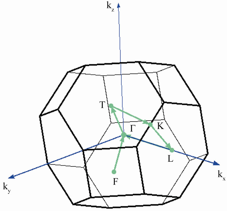
The band structure calculations of 2D MG/MnO(100) were performed using the self-consistent plane-wave pseudopotential method within the framework of density functional theory [43] (which implemented in Quantum Espresso package [44]). In the present calculations we used ultrasoft pseudopotentials with non-linear core correction. The following electron configurations for atoms were used: Mn-[Ar]3d54s2, O-[He]2s22p4, C-[He]2s22p2 (i.e., electrons in fully closed shells treated as core states). All the calculations were based on the σ-GGA spin collinear approximation using the Perdew-Burke-Ernzherof (PBE) [45] expression for the exchange-correlation functionals. All the calculations were carried out using the same unit cell dimensions. A cutoff energy of 410 eV has been chosen for the plane-wave expansion of electron states and an augmented part of the charge density has been expanded up to 2720 eV. In order to perform reciprocal space integrations we used the Monkhorst-Pack special point technique. We used a mesh of 5 × 5 × 1 special points to sample the Brillouin zone (BZ).
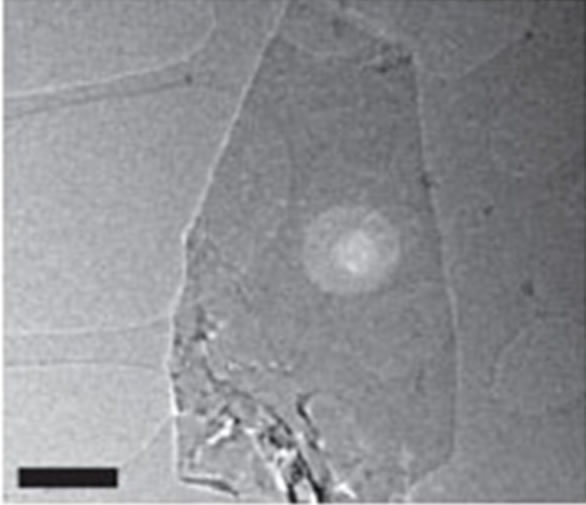
We have considered a manganese monoxide ultrathin MnO(001) layer decorated with a fragment of graphene (with torn bonds) that corresponds to an initial stage of growth of graphene film on manganese oxide. With use of transmission electron microscopy of high resolution fragments of graphene monolayers were observed [9,46]. Graphene structures are presented at Figure 1. Their analysis permits to suppose that the considered system such as “MnO(001) surface decorated with the graphene islet” shows the real situation.
In the fragment of the ultrathin graphene/MnO(001) layer presented at Figures 2(a)-(c) the graphene islet is composed of 28 carbon atoms which form 8 carbon rings with a bond length of 1.42 Å. In the atom structure of the 2D graphene/MnO(001) system a distance between the carbon rings plane and the surface layer of MnO(001) was optimized.
It is to be noted that graphene and MnO(001) have different symmetries, i.e., their compound lowers a whole system symmetry. In the process of these systems combination we centred one carbon ring at manganese atom (Figure 2(b)) of the interface layer. Then we are guided by following points: firstly graphene can be successfully
 (a)
(a) (b)
(b)
Figure 1. Electron-diffraction patterns of graphene monolayers (а) and bilayer structures (b), linear scale 500 nm [46].
synthesized on substrates with various surface crystal geometries; secondly a fundamental possibility to obtain high quality graphene sheets at gas phase without any substrates exists [9]; thirdly there is an ability of graphene sheets to totally cover disproportional parts of substrate surface [47].
It would be neutral to assume that MnO(111) surface is more preferable for graphene ordering. A mismatch of lattices between graphene and MnO(111) amounts to 4% that is less than in comparison with the MG/MnO(001) interface.
In case of the polar MnO(111) surface several variants of (111) surface reconstruction are possible. It is to note that at temperatures lower than 350˚C and oxygen pressures of  the MnO(001) layers are thermodynamically stable [31]. And only at temperatures higher than 650˚C and oxygen pressures
  a transformation of the MnO(001) surface to the polar MnO(111) surface is observed. For the MnO(111) surface a
  reconstruction has been experimentally ascertained [31].
Possible geometries of the reconstructed polar MnO(111) surface have been studied with use of the density functional theory within the bounds of PBE and PBE + U approximations [48]. It is shown that in a per-
 (a)
(a) (b)
(b) (c)
(c)
Figure 2. Geometry of the graphene/MnO(001)AF2 slab, (a) cross-sectional view, (b) top view and supercell (c).
mitted range of chemical potential values and for real partial pressures of oxygen the polar (111) surface undergoes different structural transformations (i.e., reconstruction and relaxation). Changes of electron structure, i.e., metallization is observed.
The study of possibilities of graphene ordering onto different reconstructed polar MnO(111) surfaces is not of the present work objective but an inspiration to another certain work.
In the present work properties of the MG/MnO(001) interface at room temperature are studied. At that we proceeded from the following reasons: firstly ultrathin MnO(001) layers of high structural quality have been obtained in several laboratories of the world [16,22,31]; secondly MnO(001) layers are thermodynamically stable at room temperature; thirdly we based on results of the work [47] in which it is ascertained that growing domains of graphene can cover various disproportional surfaces. It also results from the analysis of images of graphene structures presented at Figure 1(a). So our consideration of the MnO(001) surface decorated with the graphene islet reflects the real situation.
At the construction of calculation cell we proceeded from assumptions considered above. Also it is to note that our DFT-calculations for different orderings of graphene on a polar Al2O3(0001) surface have shown that band structure of interface does not change practically. So we have approached to the modeling of the graphene/MnO(001) system which is considered in the present paper.
We have modeled the ultrathin MG/MnO(001) film by a slab using a supercell approach with periodic boundary conditions. The slab included four-six layers containing 33 - 153 atoms in the supercell and each slab was separated from the other by a vacuum region not less than 8 angstrom. We did not use a dipole correction. However we have chosen sufficient vacuum region to prevent artificial electrostatic interaction between the repeated units.
We estimated stability of the MG/MnO(001)AF2 system by an average of the formation energy per atom which has been determined similarly to [31,32]

where  is full band energy calculated with use of DFT;
 ,
,  and
and  are numbers of Mn, O and C atoms within the considered layers;
 ,
,  and
and  are chemical potentials of manganese, oxygen and carbon which are equal to the cohesive energy of
  -Mn (fcc) crystal, half energy of the oxygen dimer and energy of the most stable allotrope—graphite respectively.
3. Results and Discussion
3.1. Stability of the 2D MG/MnO(001) Interface
Band calculations were preceded by the full structural optimization, i.e., this system relaxation on the basis of the density functional theory (DFT). Equilibrium positions of atoms in the supercell as well as a bond length d0 between manganese and carbon atoms in the interface of the considered system have been determined. Estimations of the formation energy of the relaxed systems of the ultrathin 2D MG/MnO(001) and 2D MnO layers have been performed for both ferroand antiferromagnetic orderings and are presented in Table 1.
So an analysis of the formation energy estimations Ef (Table 1) shows that the 2D MG/MnO(001)AF2(FM) and 2D MnO(001)AF2(FM) systems satisfy a stability condition such as Ef < 0. The calculated PBE forming energies of the systems mentioned above agree with an analogous estimation for 3D MnO AF2 [48]. This permits to predict a probable synthesis of the hypothetic material based on both antiferromagnetic ultrathin MnO film and graphene monolayer that is experimentally proved for the ultrathin MnO(001) films on various substrates [16,17,31,32,49].
3.2. Density Functional Theory Structure of 2D MG/MnO(001)FM
Dispersion  functions for the two-dimensional MG/MnO(001) and MnO systems differ significantly from analogous functions for 3D MnO that is illustrated at Figures 3 and 4. Let us analyze main features of the valence band of the 2D MG/MnO(001) system in comparison with the 2D MG and 2D MnO systems. One of the features is a near-linear character of dispersion
  curves in the Г- X direction (Figure 3(d)). Such a behavior of the dispersion curves in the Г- X direction is observed for 2D MG (Figure 3(b)) and 2D MnO (Figure 3(с)) considered here as well. The first derivative
  for the Г-X direction is rather small. Within the framework of the free electron approximation with an estimation of
 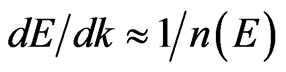 [50] a high density of electron states along the Г-X direction is ascertained. Our calculations of a local partial density of electrons in the MG/MnO(001) system prove this assumption. As we suppose these data are important for understanding of both nature and features of electron transport in the fer-
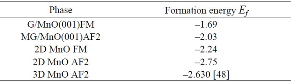
Table 1. The calculated values (PBE) of the formation energy Ef (eV/atom) of the ultrathin MG/MnO(001) and 2D MnO layers for the FM and AF2 orderings as well as of 3D MnO AF2. All values are given in eV/atom.
romagnetic heterointerface.
The valence band (VB) top of the MG/MnO(001) system is localized at the Х point for 2D Brillouin zone (Figure 2(a)) and formed by 2p-orbitals of carbon. Our energy gap calculations of MG/MnO(001) evaluate  1 eV in the indirect transition direction between the X and Г points. Let us note that the
  values for 2D MnO amount to about 2.5 eV for the direct transition at the Г point (Figure 2(c)). The band structure of 3D MnO (Figure 3) corresponds to Hubbard semiconductor. Filled electron states of VB top in the vicinity of the Г point of the MG/MnO(001) system are formed by 2p-orbitals of carbon and oxygen.
The comparison of the considered band structures permits to come to the conclusion about an appearance of C2p-Mn3d hybridization of free and filled electron states in the MG/MnO(001) system. This hybridization results in an orbital energy lowering of free C2p-orbitals of graphene more than by 2 eV that leads to their mixture with valence Mn3d-orbitals. As calculations of partial DOS have shown at Fermi level contributions of Mn3delectron states predominate (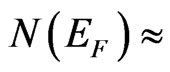 75%) over other ones such as contributions of 2p-states of oxygen. Contributions of filled C2p-states at Fermi level turn out to be less than contributions of oxygen by two orders amounting to a small value of 0.008 states/eV×atom which is comparable with known estimations [1]. The total density of states at Fermi level has amounted to a value of 2.02 states/eV×f.u. One of the most important features of this system electron spectrum is the energy position of five bands which intersect Fermi level (
 ) and essentially contribute to the total density of states at Fermi level. The last does cause the metallic type of conductivity of the ultrathin 2D MG/MnO(001)FM layer analogously to the MnO and 3D MnO systems in the ferromagnetic ordering and that corresponds to known data for 3D MnO [15].
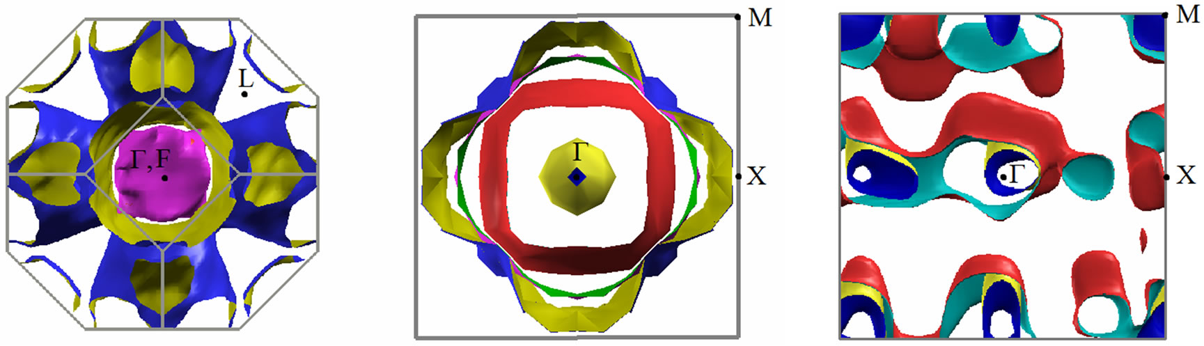
For a better understanding of Fermi surface (FS) forming regularities of the 2D MG/MnO(001)FM system in our opinion it is worthwhile to consider its transformation sequence in a row such as 3D MnO→2D MnO→ 2D MG/MnO(001). As our calculations have shown in the 3D MnO crystal Fermi surface (Figure 5(a)) is formed by sheets of three energy bands which intersect Fermi level. The fourth energy band is the widest. The sheet of Fermi surface formed by the 4th band consists of 12 electron pockets in the vicinities of the К points and is the multiply-connected unclosed surface (which shape is reminiscent of Maltese cross) where occupied states fill the k-spaces separated with yellow walls, i.e., in the Г-Х directions. Two other surfaces are formed by two similar energy bands of equal width which ones intersect Fermi level nearby the Г point. These surfaces are closed and
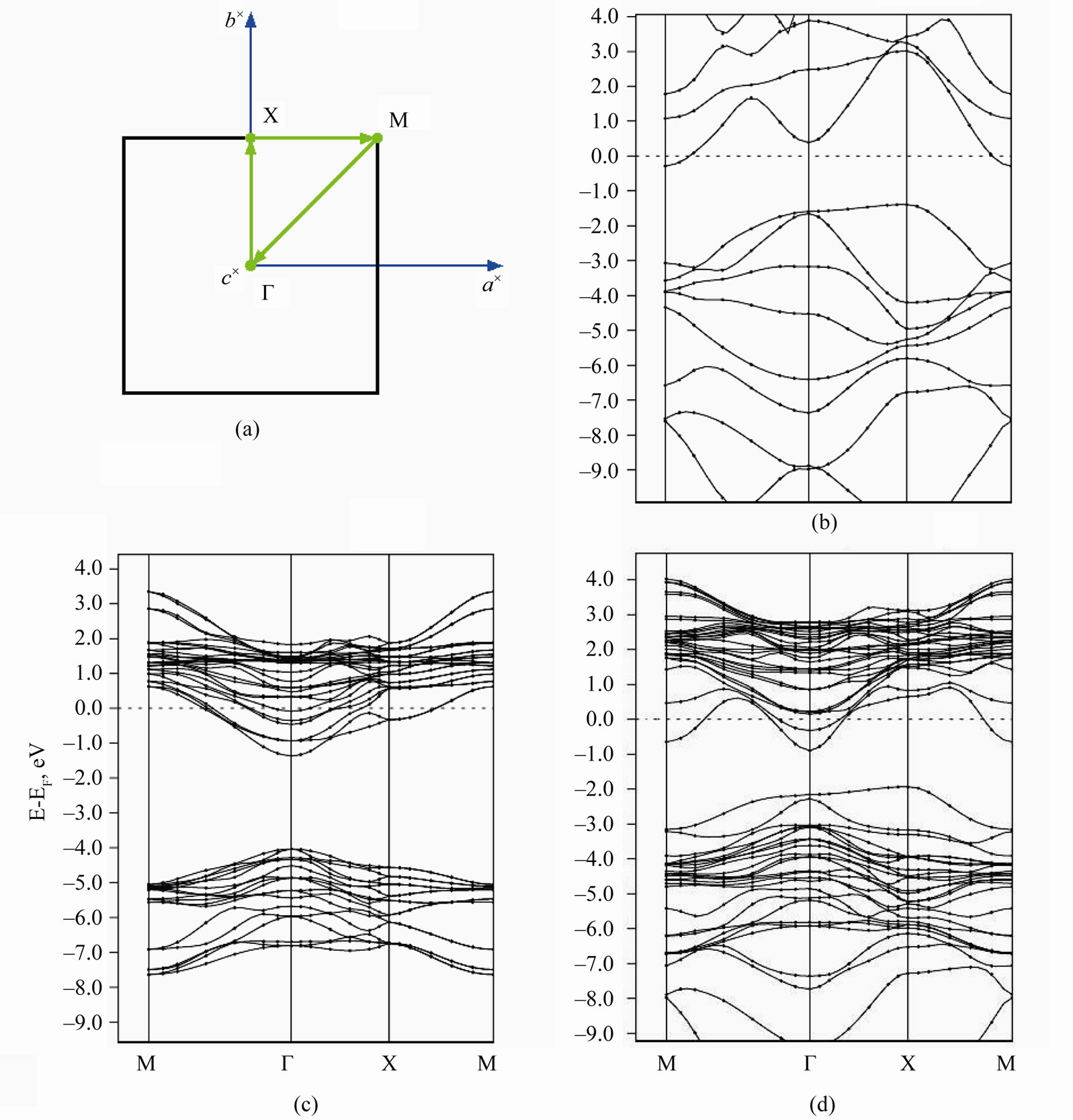
Figure 3. Brillouin zone (a) and dispersion energy functions E(k) for MG (b), 2D MnO FM (c) and 2D MG/MnO(001)FM (d). The dispersion curves (c,d) were shown with spin-down direction.
 (a)
(a) (b)
(b)
Figure 4. Brillouin zone (a) and band structure (b) of 3D MnO FM crystal.
 (a) (b) (c)
Figure 5. Fermi surface for bulk MnO (a), ultrathin 2D MnO(001) (b) and 2D MG/MnO(001) (c) layers.
filled with electrons which occupied states are localized in the vicinity of the Г point. Fermi surface is closed and electronic.
Fermi surface of the ultrathin 2D MnO FM layer (Figure 5(b)) is formed by four energy bands which intersect Fermi level. The fifth energy band is tangent to Fermi level only and therefore its sheet of Fermi surface is represented as four points which are symmetrically situated in the plane around the Г point. The first three sheets of Fermi surface are multiply-connected surfaces which embrace regions of occupied states. As one can see at Figure 5(b) the occupied electron states are mostly localized around the Г point.
It is to note that a topology of Fermi surface in the ultrathin MG/MnO(001)FM layers differs from one in the ultrathin MnO(001) layers. Fermi surface of the MG /MnO(001)FM interface is formed by two energy bands which intersect Fermi level and correspond to electron states with “spin down”. This Fermi surface is a complex multiconnected one and consists of two nonoverlapping sheets (Figure 5(c)).
As far as we know there are no published descriptions of Fermi surfaces either for the 3D MnO crystal or for the ultrathin 2D MnO layer. The qualitative description of the Fermi surface topology in the ultrathin MG/ MnO(001) and MnO(001) layers presented above will be supplemented below with a description of transport properties of charge carriers in them. In particular at Table 2 it is shown how features of Fermi surface presented at Figure 5 affect values of effective masses of charge carriers. That explains a dependence of transport properties on direction in the considered system. One can clearly see that at Figure 3 regarding an asymmetry of dispersion curves in the Г-Х and Г-М directions for the 2D MnO(001) and 2D MG/MnO(001) systems.
3.3. Density Functional Theory Structure of 2D MG/MnO(001)AF2
The band structure of the MG/MnO(001)AF2 hetero-
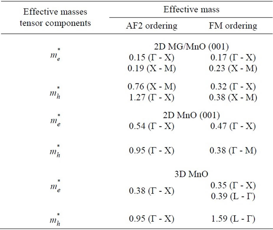
Table 2. The values of relative effective masses of electrons and holes in 2D MG/MnO (001), 2D MnO(001) and 3D MnO for both magnetic orderings and different directions in Brillouin zone.
interface is shown at Figures 6(a)-(d) in comparison with the band structure of both ultrathin MnO(001) layer and graphene for unique points of the first Brillouin zone, i.e., BZ and the chosen path. To achieve the best visualization of the comparison we have calculated the  functions for graphene (28 atoms) at the same BZ points. At Figures 6(c),(d) one can conclude that the energy band structure of 2D MG/MnO(001)AF2 is far more complicated than of 2D MnO(001). The band structure of the heterointerface (Figure 6(d)) can not be obtained by a simple superposition of carbon π-orbitals on the band structure of 2D MnO(001). This difference marked especially at the interface is in our opinion caused by an interaction of graphene
 ![]() -band states with surface manganese d-states mostly.
-band states with surface manganese d-states mostly.
For 2D MnO(001) it is obvious that the conduction band bottom is at the Г point and formed by antibonding manganese s-states. As the characteristic feature of the valence band top of 2D MnO(001) is the presence of a
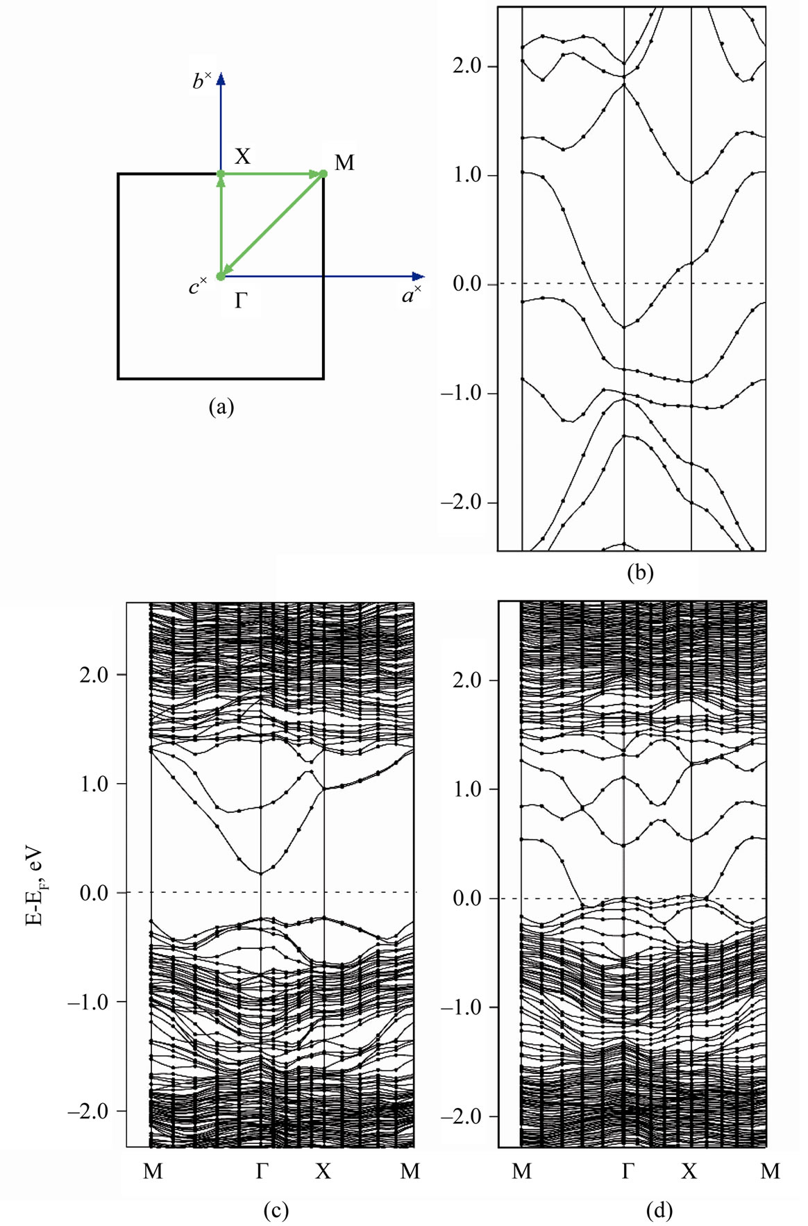
Figure 6. Brillouin zone (a) and dispersion energy E(k) functions for MG (b), 2D MnO AF2 (c) and 2D MG/MnO(001)AF2 (d).
large amount of local maxima in the Г-Х direction. The valence band top is occupied mostly with the surface manganese d-states which are splitted near Fermi level. According to our calculations the ultrathin MnO(001) layer is a direct band semiconductor because the absolute minimum of the conduction band as well as maximum of the valence band are realized at the Г point. The calculated energy gap values for 2D MnO(001), i.e.,  = 0.6 eV.
Let us note that an interaction between graphene and substrate is observed for the equilibrium 2D MG/ MnO(001)AF2 system. The bond length between graphene carbon atoms and manganese ones in the substrate (001) plane, i.e.,  = 2.525 Å. This estimation is near to an experimental value such as
 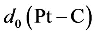 = 2.45 Å for the MG/Pt(111) system [51]. The interaction between graphene and substrate is possible due to a hybridization of graphene
 ![]() -band states with surface bonding d-states of Mn in the M-Г and M-X directions of the wave vector that results in a formation of interface states at Fermi level. The above mentioned interaction reduces to a nonrigid shift of occupied electron states forming the valence band top of 2D MG/MnO(001)AF2 by 0.25 eV relative to Fermi level
-band states with surface bonding d-states of Mn in the M-Г and M-X directions of the wave vector that results in a formation of interface states at Fermi level. The above mentioned interaction reduces to a nonrigid shift of occupied electron states forming the valence band top of 2D MG/MnO(001)AF2 by 0.25 eV relative to Fermi level .
.
As our calculations have shown the energy structure at Fermi level is formed by the electron  - and
- and  -orbitals of the interface MnO(001) layer as well as by
  -orbitals of graphene carbon. The density of electron states at Fermi level has amounted to a value of about
  states/eV∙form.unit. However contributions of the manganese
  -orbitals to energy bands of the valence band top are determinative. According to our calculations one observes also a hybridization of graphene
 ![]() -bands with antibonding manganese s-states in the conduction band in the Г-X and Г-M directions that reduces to a formation of hybridized bands in the energy range of 0.5 - 1.5 eV and is accompanied with the shift of
-bands with antibonding manganese s-states in the conduction band in the Г-X and Г-M directions that reduces to a formation of hybridized bands in the energy range of 0.5 - 1.5 eV and is accompanied with the shift of ![]() -bands of graphene by a value of
-bands of graphene by a value of  ~0.5 eV relative to Fermi level.
It is noteworthy that the dispersion  curves for the two-dimensional MG/MnO(001) and MnO(001) systems (Figures 6(c,d)) differ significantly from
  for the 3D MnO crystal (Figure 7(b)).
In particular according to our calculations the dimension lowering of the considered systems is characterized by the partial degeneration of the  energy as well as removal of the
  and
and  sublevels splitting (due to an octahedral crystal field). For the 3D MnO AF2 crystal it is typical that the dispersion
  curves forming the valence band are in the energy range of –(8.0 - 0.5) eV and splitted into four bands in accordance with known theoretical and experimental results [15,23,24].
3.4. Transport and Magnetism in the Ferromagnetic MG/MnO(001) Heterointerface
It is known [52,53] that at room temperature and at the metal/dielectric border for barriers in the range of 1.5 - 4.0 eV the charge carriers injection into the dielectric comes to be in accordance with the tunnel mechanism of Fowler-Nordheim (FN) [52]. As well as it is known that in the Si/Al2O3 and Si/ZrO2 heterostructures the barrier value amounts to 2.0 eV [54]. Silicon and carbon have the isoelectron structure. As graphene is characterized by the metallic conductivity then owing to fact that silicon and carbon atoms are isoelectronic it is possible to state that the barrier for MG/MnO(001) can amount to a value of the same order as in Si/ZrO2 [54]. In this case the charge transfer through the MG/MnO(001) barrier can be carried out according to the FN mechanism and a value of the tunnel injective current exponentially depends on a value of the effective masses of electrons and holes in the studied 2D structure.
The tensor components of the effective masses of electrons and holes have been determined as in [53,55] using the relation
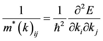
where  - effective mass of carrier,
  -wave vector, and
  -Plank constant. In Table 2 we show the calculated values of the effective masses for electrons and
 (a)
(a)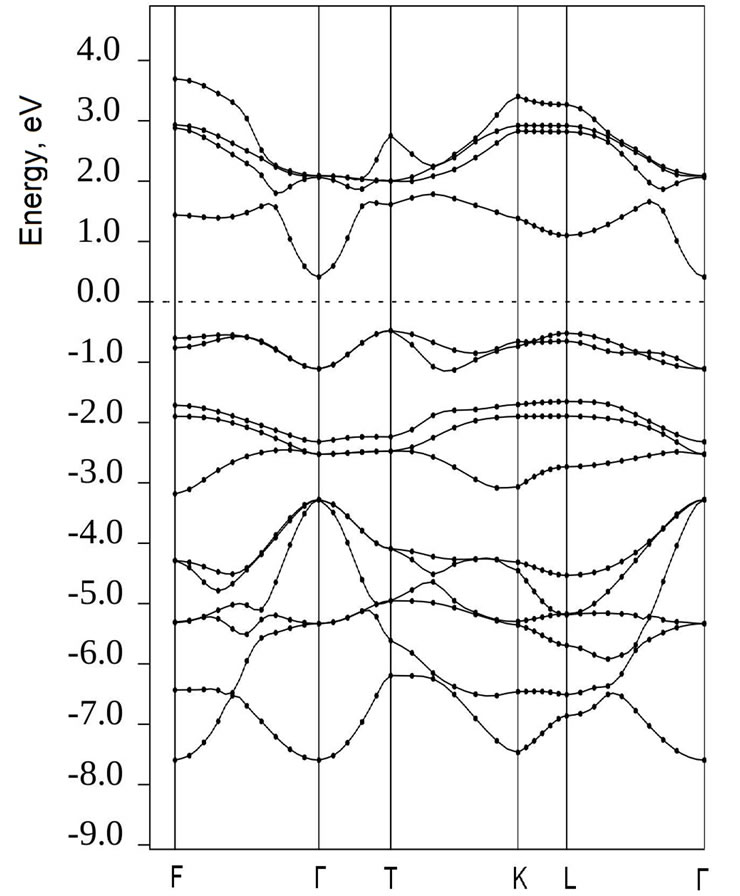 (b)
(b)
Figure 7. Brillouin zone (a) and band structure (b) of the 3D MnO AF2 crystal.
holes in the interface of the ultrathin MG/MnO(001) and MnO(001) layers for the ferromagnetic and antiferromagnetic orderings. These values are compared with estimations of the effective masses for 3D MnO obtained in the same approximation. It is to be noted that effective masses of carriers were determined using the dispersion  curves, i.e., by their extremums parabolic approximation nearby Fermi level. Hereupon an estimation of the
  value has turned out to be possible only for that directions in Brillouin zone where the
  functions had the extremums nearby Fermi level
 .
.
According to band calculations the effective masses of electrons for various directions in Brillouin zone of the considered systems are in the range of (0.15 - 0.54)  and are typical for dielectrics such as Al2O3, SiO2, Si3N4 and HfO2 [56-58]. The calculated values of the effective masses of electrons in the 3D MnO crystal are equal for different directions (Table 2) and are near to experimenttal data, e.g.,
  ~ 0.39
 for 3D ZnS [59]. In the ultrathin MnO(001) layer the effective masses of electrons at the Г point in the Г-X direction amount to a value of about 0.50
 . In the MG/MnO(001) heterostructure the effective masses of electrons in the Г-X direction are more than two times less than in the 3D MnO crystal.
It is notable that local geometry anomalies of Fermi surface (Figure 5) qualitatively correlate with the difference between values of effective masses of charge carriers (Table 2). As a result an anisotropy of the transport properties appears in the considered systems.
The tensor components of the effective masses of holes in the two-dimensional MG/MnO(001) and MnO (001) systems as well as in the 3D MnO crystal are in the range of (0.38 - 1.59) . The mobility estimation of electrons and holes
  can be performed similarly to the work [60]

where ![]() -relaxation time in the system (
-relaxation time in the system ( ) [60]. The calculations have shown that the mobilities of electrons and holes amount to
  and
and 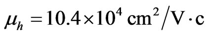 respectively. Hence one can draw a conclusion that in the present system the mobility of carriers, specifically holes, is almost by 10 times higher than of two-dimensional holes in Ge-layers of the Ge-Ge1–xSix heterostructure (
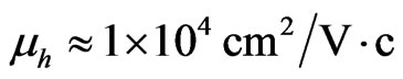 [60]). The mobility of electrons in 2D MG/MnO(001)AF2 amounts to
 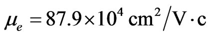 and is also the higher-order one than the mobility of two-dimensional electrons in the GaAs/AlGaAs heterostructures (
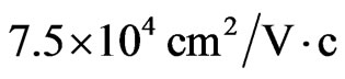
 [60]) for concentrations such as
 .
.
So in the two-dimensional MG/MnO(001) and MnO (001) systems one observes different transport properties of carriers in a layer of nanometer thickness. In the ferromagnetic MG/MnO(001) heterointerface transport properties of carriers (electrons and holes) have turned out to be of the higher-order than in known heterostructures [60,61].
For the studied systems an integration of electron partial density ρ(r) for both spin projections has permitted to obtain comparable data on partial charges of valence electrons at atoms, specifically for 2D MG/MnO(001) and 3D MnO (Table 3), as well as to determine an integral spin magnetic moment (ММ) at every atom (Table 4). Estimations of Qeff values based on the atomic effective charge concept [62,63] have been performed (Table 4). An analysis of the estimations permits to calculate a charge transfer to the Mn-O bond that amounts to ~0.50е. It is possible to suppose that an additional charge transfer from manganese atoms to atom of carbon exists and amounts to ~0.04 е.
The calculations have shown that in the 2D MG/ MnO(001)FM system along with the magnetic moment at the Mn+2 ion (4.42 μB) there are spin magnetic moments at atoms of carbon (–0.10 µB) and oxygen (0.19 μB). An occurrence of magnetic moments at carbon atoms (0.74 μB) has been previously observed in BeO:C [65], in ZnO:C films [66] and in purely-carbon nanosystems [67].
The nature of formation of magnetic properties of carbon in the BeO:C system authors of the work [65] link to a mutual arrangement of the matrix valence
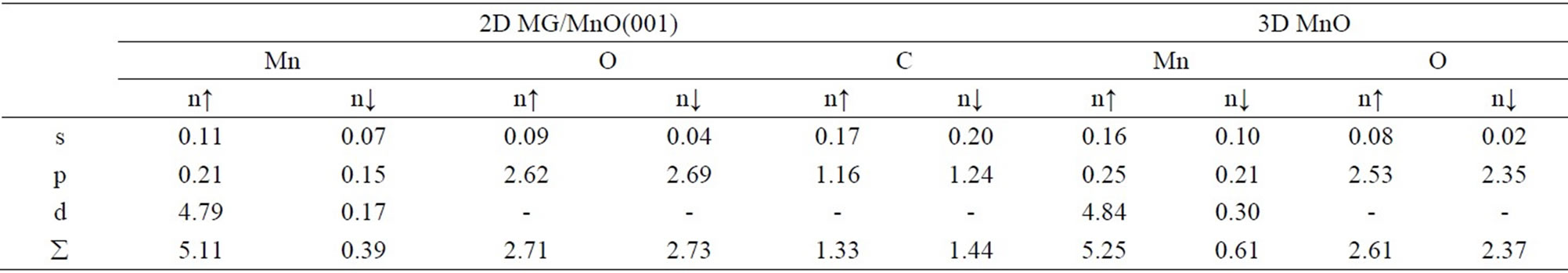
Table 3. The partial and spin distribution of valence electrons at atoms for the 2D MG/MnO(001)FM and 3D MnO FM systems.
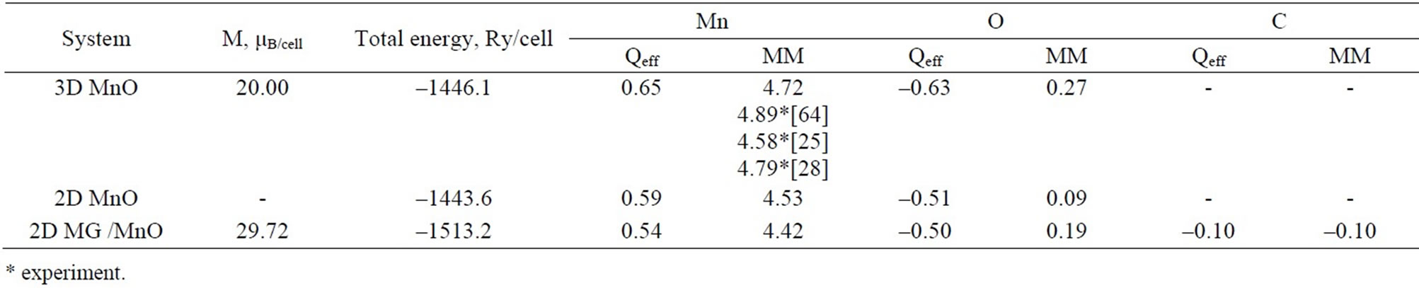
Table 4. The total magnetization (M), total energy-per-cell (Ry/cell), effective charges Qeff (е) and magnetic moments (MM, μB) at atoms in MnO and MG /MnO in the case of ferromagnetic ordering.
O2p-band and 2p-band of the doping carbon atom in the energy spectrum of BeO:C that results in a spontaneous spin-polarization of C (2p↑ – 2p↓)-states. The analysis of the partial DOS for atoms of Mn, O and C of the 2D MG/MnO(001) system in the FM ordering (Figure 8) reveals a dominant role of the spontaneous spin polarization of Mn 3d and 2p-orbitals of atoms of oxygen and carbon.
It should be noted that according to our calculations the local density of electron states of atoms in monolayers in the (001) direction of the 2D MG/MnO system is not homogenous. This can cause a difference in magnetic states of atoms of manganese and oxygen in the layers. In the antiferromagnetic ordering the two-dimensional MG/MnO(001) system does not have a total magnetic moment. It is confirmed by the total density of electron states that is presented in Figure 9. It has been found that every atom of Mn in 2D MG/MnO(001) has its own magnetic moment by the value of 4.52 µB with the opposite spin orientation in the parallel (111) planes and the main contribution into the magnetic moment is due to the Mn 3d-orbitals. The magnetic moment value is near to an analogous estimation for the manganese atom (4.4 µB) in thin layers of (Zn, Mn)O [68] and has turned out to be insignificantly lower than our estimation for the 3D MnO AF2 crystal (4.54 µB).
The results obtained in the present paper are in a satisfactory correspondence to an experiment [27,28]. The decrease nature of the magnetic moment at manganese atom in comparison with the MnO dimer (5.0 µB) one links to the hybridization between O2p4- and Mn3d5- states [68]. The calculations performed in this paper have shown that in the 2D MG/MnO(001) system along with the magnetic moment of the Mn+2 ion the small magnetic spin moments for atoms of oxygen (0.04 µB) as well as carbon (0.05µB) are revealed. The formation of the small magnetic moments was earlier observed at oxygen atom in thin films of (Zn,Mn)O (0.14 µB) [68] as well as in the nonmagnetic SrTiO2.875N0.125 perovskite (0.04 μB) [69] and at carbon atom in the TcCNi3 antiperovskite (0.026 μB) [70] as well as in the graphene MG/SiC(0001) buffer layer (0.02 µB) [36].
The analysis of the partial DOS for atoms of Mn, O and C (Figure 10) in the two-dimensional MG/MnO(001) system has shown that the spontaneous spin polarization of the manganese 3dand oxygen 2p-orbitals with an admixture of the carbon 2p-ones plays the dominant role in the formation of the magnetic moments at atoms.
Our estimations of the magnetic moment value at carbon atoms have shown that the total magnetic moment of graphene islet formed by 28 atoms amounts to 0.28 µB. The analysis shows that the little magnetic moment at carbon atom amounts to: ~ 0 µB (14%); 0.01 μВ (58%);
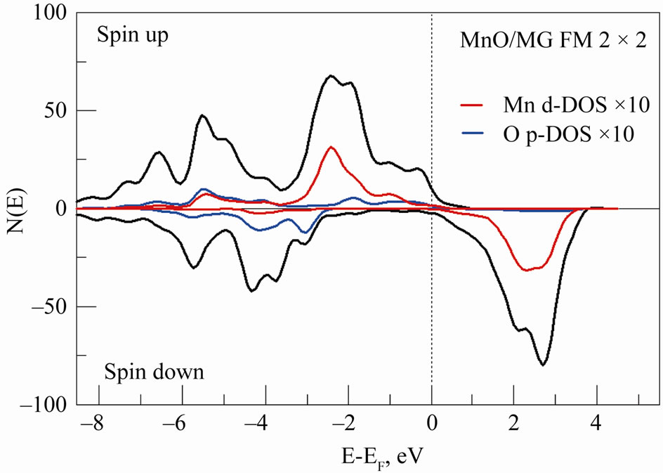
Figure 8. Total (black) and partial DOS for atoms of Mn (red) and O (blue) in the 2D MG/MnO(001)FM system. Total DOS per 2 × 2 × 1 supercell and partial DOS for single atoms of Mn and O are shown, multiplied by 10.
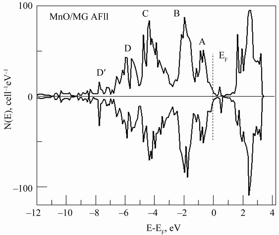
Figure 9. Total DOS for the 2D MG/MnO AF2 system per supercell is shown.
0.02 μВ (21%) and 0.03 μВ (7%). The distribution of the magnetic moments at carbon atoms is presented in Figure 11. It is known that the so-called “flickering” magnetism in graphene may be caused by topological defects, adsorbed substances, doping atoms, “zigzag” edge [62,64] or induced by the substrate [36]. Due to the band structure analysis of the graphene/MnO(001) system above we have drawn a conclusion of the formation of the C2p-Mn3d-hybridization of free and filled states. As a result of the pd-hybridization the orbital energy of free electron 2p-states of carbon in graphene lowers that reduces to these states admixture to valence 3d-states of manganese in the ultrathin MnO(001) layer and to the topology change of Fermi surface. This circumstance may be responsible for the “flickering” magnetism formation in graphene of the 2D graphene/MnO(001) sys-
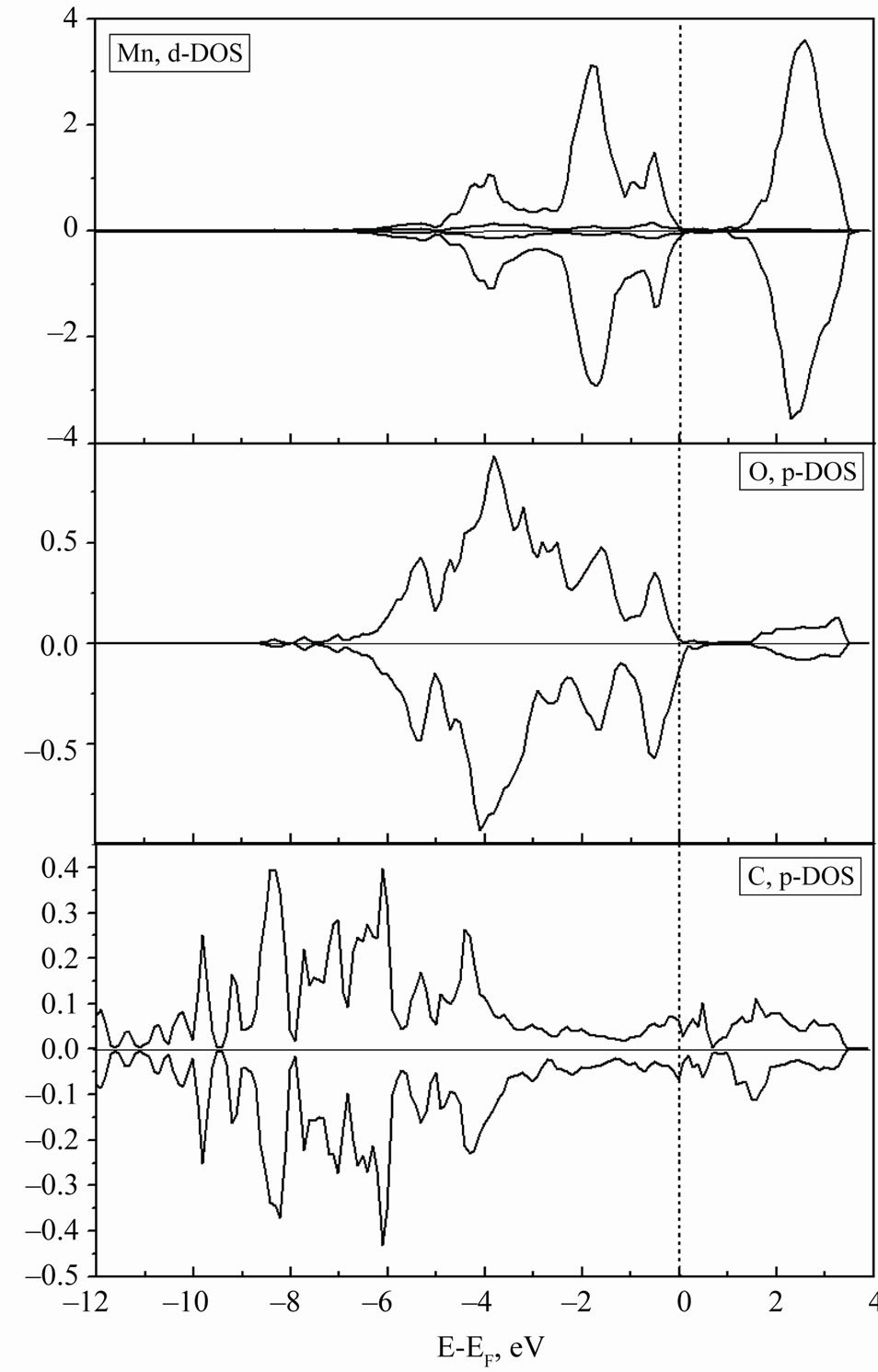
Figure 10. Partial DOS for single atoms of Mn, O and C.

Figure 11. Value distribution map of magnetic moments at carbon atoms (1,2,3) in graphene monolayer.
tem. Noteworthy that in graphene the magnetism revealed in the present paper is induced by the MnO(001) substrate as the pd-hybridization result.
Several carbon atoms at the margin (“zigzag” type) of the graphene islet turn out to be nonmagnetic (or almost nonmagnetic with magnetic moment less than 0.005 μВ) and within the bounds of authors’ concept [36] one can suppose that these atoms have a sp3-configuration as well as take part in a formation of bond with the substrate. This interpretation corresponds to authors’ assumption of the paper [51] that only the carbon atoms at the margin of the graphene islet can form chemical bonds with the substrate. It is to be noted that in the optimized atom graphene/MnO(001) structure bond lengths such as Mn-C and С-O amount to  = 2.591 Å and
 ![]() = 2.580 Å respectively that is not typical for the sp3-hybridization.
= 2.580 Å respectively that is not typical for the sp3-hybridization.
On the total electron density mapping (Figure 12) one can see some features of interatomic С-С-interactions within the bounds of the both islet model and Mn3dC2p-interaction presence in the system interface. We should note the electron density localization along the С-С lines which one is typical for a sp2-configuration as well as caused by the interaction between carbon atoms with a bond length of 1.42 Å.
4. Conclusions
Using the spin-polarized full-potential method of pseudopotential within the framework of the density functional theory (DFT) for the 2D MG/MnO(001) and 2D MnO(001) systems in the antiferromagnetic and ferromagnetic orderings the band structure has been investigated and both phase stability forecast and analysis of electron and magnetic properties as well as chemical bond nature have been performed.
The determined anisotropic character of the electron structure in the dimensional quantization direction of the ultrathin 2D MG/MnO(001) AF2 layer can cause the difference in magnetic states of atoms of Mn and O. In

Figure 12. Total electron density mapping for the two-dimensional graphene/MnO(001) system in the (001) section.
the present system for the first time the magnetic moment estimations at Mn+2 ion have been theoretically performed. The spontaneous spin polarization effect of Mn 3d and 2p-bands of atoms of oxygen and carbon in the 2D MG/MnO(001) system has been revealed which one in our opinion plays the dominant role in the magnetic moments formation of atoms of Mn and O. Electron energy structure features of bands in the vicinity of Fermi level determine the graphene layer magnetism in the two-dimensional MG/MnO(001) AF2 system. Our ab initio estimations of magnetic moments of carbon atoms have shown that: firstly for the graphene sheet which consists of 28 carbon atoms the total magnetic moment (algebraic sum) amounts to 0.02µB per supercell; secondly the magnetic moments directions of two equivalent carbon sublattices such as A and B are opposite [1,8]; thirdly some carbon atoms at the margin (of the considered fragment of the graphene sheet) are nonmagnetic because they take part in a chemisorptive bond formation with the substrate. The chemical bond formation between graphene and the substrate can result in a replacement of the electron  -configuration by the
  -type for some carbon atoms. As an indirect proof of the mentioned bond can be: firstly an additional D’ (Figure 9) band formation with a width of 1.7 eV that in comparison with 2D MnO one can consider as a sp-hybridization result caused by both
  - and
- and  -orbitals (Figure 10) mixing; secondly the strong covalent sp-bond existence for electrons of carbon atoms and manganese ones is revealed by their local partial density of electron states. This interpretation correlates with known physical notions.
For the first time it has been shown that Fermi surface topologies in the 2D MG/MnO(001)FM heterostructure and ultrathin MnO(001)FM layers as well as in the 3D MnO FM crystal are different that determines the difference of transport properties of these systems carriers.
The effective masses and the mobility of charge carriers in the two-dimensional MG/MnO(001) and MnO(001) structures have been theoretically calculated for the first time as well. The effective masses of both electrons and holes for different directions in BZ are in the ranges of (0.15 - 0.54) and (0.38 - 1.27)
 respectively. In the MG/MnO(001)AF2 heterostructure the mobility of electrons (
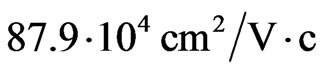 ) is 10 times higher than the mobility of two-dimensional electrons of the GaAs/ AlGaAs heterostructure [60]. The holes mobility
  has turned out to be the higherorder one than the mobility of two-dimensional holes in the Ge-layers of the Ge-Ge1-xSix heterostructure [60]. The essential anisotropy of electron and hole masses in two-dimensional structures such as MG/MnO(001) and MnO(001) shall determine the carriers transport properties in the layer of nanometer thickness.
Thus on the basis of the formation energy  calculations of the ferromagnetic MG/MnO(001) heterointerface the successful synthesis possibility of new materials of this type has been shown. The recent experiments [17,22] have demonstrated possibilities to obtain epitaxial ultrathin layers of manganese monoxide as well as graphene sheets on surface with different crystal geometries. Therefore the obtained data on the transport properties as well as the magnetism nature in the ferromagnetic graphene/MnO(001) heterointerface can be considered as the possible base for implementations in devices of spintronics.
REFERENCES
- K. S. Novoselov, A. K. Geim, S. V. Morozov, D. Jiang, Y. Zhang, S. V. Dubonos, I. V. Grigorieva and A. A. Firsov, “Electric Field Effect in Atomically Thin Carbon Films,” Science, Vol. 306, No. 5696, 2004, pp. 666-669. doi:10.1126/science.1102896
- Y. Zhang, Y.-W. Tan, H. L. Stormer and P. Kim, “Experimental Observation of the Quantum Hall Effect and Berry’s Phase in Graphene,” Nature, Vol. 438, 2005, pp. 201-204. doi:10.1038/nature04235
- K. S. Novoselov, A. K. Geim, S. V. Morozov, D. Jiang, M. I. Katsnelson, I. V. Grigorieva, S. V. Dubonos and A. A. Firsov, “Two-Dimensional Gas of Massless Dirac Fermions in Graphene,” Nature, Vol. 438, No. 7065, 2005, pp. 197-200. doi:10.1038/nature04233
- A. K. Geim and A. H. MacDonald, “Graphene: Exploring Carbon Flatland,” Physics Today, August 2007. http://www.physicstoday.org
- M. Freitag, “Graphene: Nanoelectronics Goes Flat Out,” Nature Nanotechnology, Vol. 3, No. 8, 2008, pp. 455-457. doi:10.1038/nnano.2008.219
- X. Wu, M. Sprinkle, X. Li, F. Ming, C. Berger and W. A. Heer, “Epitaxial-Graphene/Graphene-Oxide Junction: An Essential Step towards Epitaxial Graphene Electronics,” Physical Revive Letters, Vol. 101, 2008, pp. 026801-1-4.
- M. I. Katsnelson, “Graphene: Carbon in Two Dimensions, Review,” Materials Today, Vol. 10, No. 1-2, 2007, pp. 20-27. doi:10.1016/S1369-7021(06)71788-6
- С. V. Morozov, K. C. Novoselov and А. K. Geim, “Electron Transport in Graphene,” Physics-Uspekhi, Vol. 178, 2008, pp. 776-780.
- A. Dato, V. Radmilovic, Z. Lee, J. Phillips and M. Frenklanch, “Substrate-Free Gas-Phase Synthesis of Graphene Sheets,” Nano Letters, Vol. 8, No. 7, 2008, pp. 2012-2016. doi:10.1021/nl8011566
- N. Tombros, C. Jozsa, M. Popincius, N. T. Jonkman and B. J. Wees, “Electronic Spin Transport and Precession in Single Grapheme Layers at Room Temperature,” Nature, Vol. 448, No. 7153, August 2007, pp. 571-574. doi:10.1038/nature06037
- S. Cho, Yu.-F. Chen and M. S. Fuhrer, “Gate-Tunable Graphene Spin Valve,” Applied Physics Letters, Vol. 91, 2007, pp. 123105-1-3. doi:10.1063/1.2784934
- M. Ohishi, M. Shiraishi, R. Nouchi, T. Nozaki, T. Shinjo and Y. Suzuki, “Spin Injection into a Graphene Thin Film at Room Temperature,” Japanese Journal Applied Physics, Vol. 46, 2007, pp. L605-L607. doi:10.1143/JJAP.46.L605
- R. Fiederling, M. Keim, G. Reuscher, W. Ossau, G. Sehmidt, A. Waag and L. W. Molenkamp, “Injection and Detection of a Spin-Polarized Current in a Light-Emitting Diode,” Nature, Vol. 402, No. 6763, 1999, pp. 787-790. doi:10.1038/45502
- A. Leuliet, A. Vasanelli, A. Wade, G. Fedorov, D. Smirnov, G. Bastard and C. Sirtori, “Electron Scattering Spectroscopy by a High Magnetic Field in Quantum Cascade Lasers,” Physical Review B, Vol. 73, 2006, pp. 085311- 1-9. doi:10.1103/PhysRevB.73.085311
- J. E. Pask, D. J. Singh, I. I. Mazin, C. S. Hellberg and J. Kortus, “Structural, Electronic and Magnetic Properties of MnO,” Physical Review B, Vol. 64, 2001, pp. 024403- 1-7.
- F. Müller, R. de Masi, D. Reinicke, P. Steiner, S. Hüfner and K. Stöwe, “Epitaxial Growth of MnO/Ag(001) Films,” Surface Science, Vol. 520, No. 3, 2002, pp. 158- 172. doi:10.1016/S0039-6028(02)02268-9
- W. Neubeck, L. Ranno, M. B. Hunt, C. Vettier and D. Givord, “Epitaxial MnO Thin Films Grown by Pulsed Laser Deposition,” Applied Surface Science, Vol. 138- 139, January 1999, pp. 195-198. doi:10.1016/S0169-4332(98)00421-8
- S. I. Csiszar, M. W. Haverkort, Z. Hu, A. Tanaka, H. H. Hsieh, H.-J. Lin, C. T. Chen, T. Himba and L. H. Tjeng, “Controlling Orbital Moment and Spin Orientation in CoO Layers by Strain,” Physical Review Letters, Vol. 95, 2005, pp. 187205-1-4. doi:10.1103/PhysRevLett.95.187205
- R. Abrudan, J. Miguel, M. Bernien, C. Tieg, M. Piantek, J. Kirschner and W. Kuch, “Structural and Magnetic Properties of Epitaxial Fe/CoO Bilayers on Ag(001),” Physical Review B, Vol. 77, 2008, pp. 014411-1-7. doi:10.1103/PhysRevB.77.014411
- S. I. Csiszar, M. W. Haverkort, T. Burnus, Z. Hu, A. Tanaka, H. H. Hsieh, H.-J. Lin, C. T. Chen, J. C. Cezar, N. B. Brookes, T. Himba and L. H. Tjeng, “Aligning Spins in Antiferromagnetic Films Using Antiferromagnetics,” 2008, arXiv: cond-mat/0504520v2.
- K. R. Nikolaev, A. Yu. Dobin, I. N. Krivorotov, W. K. Cooley, A. Bhattacharya, A. L. Kobrinskii, L. I. Glazman, R. M. Wentzovitch, E. Dan Dahlberg and A. M. Goldman, “Oscillatory Exchange Coupling and Positive Magnetoresistance in Epitaxial Oxide Heterostructure,” Physical Review Letters, Vol. 85, No. 17, 2000, pp. 3728-3731. doi:10.1103/PhysRevLett.85.3728
- A. Chassé, Ch. Langheirch, F. Müller and S. Hüfner, “Growth and Structure of Thin MnO Films on Ag(001) in Dependence on Film Thickness,” Surface Science, Vol. 602, No. 2, 2008, pp. 597-606. doi:10.1016/j.susc.2007.11.014
- M. Nagel, I. Biswas, H. Peisert and T. Chassé, “Interface Properties and Electronic Structure of Ultrathin Manganese Oxide Films on Ag(001),” Surface Science, Vol. 601, No. 18, 2007, pp. 4484-4487. doi:10.1016/j.susc.2007.04.137
- T. Oguchi, K. Terakura and A. R. Williams, “Band Theory of the Magnetic Interaction in MnO, MnS, and NiO,” Physical Review B, Vol. 28, 1983, pp. 6443-6453. doi:10.1103/PhysRevB.28.6443
- Z. Fang, I. V. Solovyev, H. Sawada and K. Terakura, “First-Principles Study on Electronic Structure and Phase Stability of MnO and FeO under High Pressure,” Physical Review B, Vol. 59, No. 2, 1999, pp. 762-774. doi:10.1103/PhysRevB.59.762
- C. Franchini, R. Podloucky, J. Paier, M. Marsman and G. Kresse, “Graund-State Properties of Multivalent Manganese Oxides: Density Functional and Hybrid Density Functional Calculation,” Physical Review B, Vol. 75, 2007, pp. 195128-1-11. doi:10.1103/PhysRevB.75.195128
- A. K. Cheetham and D. A. O. Hope, “Magnetic Ordering and Exchange Effect in the Antiferromagnetic Solid Solutions MnxNi1–xO,” Physical Review B, Vol. 27, No. 11, 1983, pp. 6964-6967. doi:10.1103/PhysRevB.27.6964
- D. E. F. Fender, A. J. Jacobson and F. A. Wegwood, “Covalency Parameters in MnO, Alpha-MnS, and NiO,” Journal Chemical Physics, Vol. 48, 1968, pp. 990-994. doi:10.1063/1.1668855
- D. Kasinathan, J. Kuneš, K. Koepernik, C. V. Diaconu, R. L. Martin, I. D. Prodan, G. E. Scuseria, N. Spaldin, L. Petit, T. C. Schulthess and W. E. Pickett, “Mott Transition of MnO under Pressure: A Comparison of Correlated Band Theories,” Physical Review B, Vol. 74, 2006, pp. 195110-1-12. doi:10.1103/PhysRevB.74.195110
- V. V. Ilyasov, I.V. Ershov, I. Ya. Nikiforov, D. A. Velikozkii and T. P. Zhdanova, “Localized Electron States and Magnetic Properties at the Interface of a Two-Dimensional Grapheme/MnO(001) System,” Journal Surface Investigation: X-Ray, Synchrotron and Neutron Techniques, Vol. 5, No. 4, 2011, pp. 754-763.
- F. Allegretti, C. Franchini, V. Bayer, M. Leitner, G. Parteder, B. Xu, A. Fleming, M. G. Ramsey, R. Podloucky, S. Surnev and F. P. Netzer, “Epitaxial Stabilization of MnO(111) Overlayers on a Pd(100) Surface,” Physical Review B, Vol. 75, 2007, pp. 224120-1-8. doi:10.1103/PhysRevB.75.224120
- C. Franchini, R. Podloucky, F. Allegretti, F. Li, G. Parteder, S. Surnev and F. P. Netzer, “Structural and Vibrational Properties of Two-Dimentional MnxOy Layers on Pd(100): Experiments and Density Functional Theory Calculations,” Physical Review B, Vol. 79, 2009, pp. 035420-1-12. doi:10.1103/PhysRevB.79.035420
- Ch. Hagendorf, S. Sachert, B. Bochmann, K. Kostov and W. Widdra, “Growth, Atomic Structure, and Vibrational Properties of MnO Ultrathin Films on Pt(111),” Physical Review B, Vol. 77, 2008, pp. 075406-1-9. doi:10.1103/PhysRevB.77.075406
- H. L. Lu, G. Scarel, X. L. Li and M. Fanciulli, “Thin MnO and NiO Films Grown Using Atomic Layer Deposition from Ethylcyclopentadienyl Type of Precursors,” Journal Crystal Growth, Vol. 310, No. 24, 2008, pp. 5464-5468. doi:10.1016/j.jcrysgro.2008.08.031
- A. M. Shikin, S. A. Gorovikov, V. K. Adamchuk, W. Gudat and O. Rader, “Electronic Structure of Carbon Nanostripes,” Physical Review Letters, Vol. 90, 2003, pp. 256803-1-4. doi:10.1103/PhysRevLett.90.256803
- A. Ramasubramaniam, N. V. Medhekar and V. B. Shenov, “Substrate-Induced Magnetism in Epitaxial Grapheme Buffer Layers,” Nanotechnology, Vol. 20, 2009, Article ID 275705, pp. 1-7. doi:10.1088/0957-4484/20/27/275705
- G. Bertoni, L. Calmels, A. Altibelli and V. Serin, “First-Principles Calculation of the Electronic Structure and EELS Spectra at the Grapheme/Ni(111) Interface,” Physical Review B, Vol. 71, 2004, pp. 075402-1-8. doi:10.1103/PhysRevB.71.075402
- E. H. Hwang, S. Adam and S. D. Sarma, “Carrier Transport in Two-Dimensional Graphene Layers,” Physical Review Letters, Vol. 98, 2007, pp. 186806-1-4. doi:10.1103/PhysRevLett.98.186806
- J. Nilsson and A. H. C. Neto, “Impurities in a Biased Graphene Bilayer,” Physical Review Letters, Vol. 98, 2007, pp. 126801-1-4. doi:10.1103/PhysRevLett.98.126801
- A. H. C. Neto, F. Guinea and N. M. R. Peres, “Edge and Surface States in the Quantum Hall Effect in Graphene,” Physical Review B, Vol. 73, 2006, pp. 205408-1-8. doi:10.1103/PhysRevB.73.205408
- J. Nilsson, A. H. C. Neto, F. Guinea and N. M. R. Peres, “Transmisson through a Biased Grapheme Bilayer Barrier,” November 2007, arXiv:cond-mat/0607343v2 26
- Y. Wang, Yu. Huang, Y. Song, X. Zhang, Y. Ma, J. Liang and Y. Chen, “Room-Temperature Ferromagnetism of Graphene,” Nano Letters, Vol. 9, No. 1, 2009, pp. 220- 224. doi:10.1021/nl802810g
- W. Kohn and L. J. Sham, “Self-Consistent Equations including Exchange and Correlation Effects,” Physical Review, Vol. 140, No. 4A, 1965, pp. A1133-A1138. doi:10.1103/PhysRev.140.A1133
- P. Giannozzi, S. Baroni, N. Bonini, M. Calandra, R. Car, C. Cavazzoni, D. Ceresoli, G. L. Chiarotti, M. Cococcioni, I. Dabo, A. D. Corso, S. Gironcoli, S. Fabris, G. Fratesi, R. Gebauer, U. Gerstmann, C. Gougoussis, A. Kokalj, M. Lazzeri, L. Martin-Samos, N. Marzari, F. Mauri, R. Mazzarello, S. Paolini, A. Pasquarello, L. Paulatto, C. Sbraccia, S. Scandolo, G. Sclauzero, A. P. Seitsonen, A. Smogunov, P. Umari and R. M. Wentzcovitch, “Quantum Espresso: A Modular and Open-Source Solfware Project for Quantum Simulations of Materials,” Journal Physics: Condensed Matter, Vol. 21, 2009, pp. 395502-1-8. doi:10.1088/0953-8984/21/39/395502
- J. P. Perdew, S. Burke and M. Ernzerhof, “Generalized Gradient Approximation Made Simple,” Physical Review Letters, Vol. 77, No. 18, 1996, pp. 3865-3868. doi:10.1103/PhysRevLett.77.3865
- Y. Hernandez, V. Nicolosi, M. Lotya, F. M. Blighe, Z. Sun, S. De, I. T. McGovern, B. Holland, M. Byrne, Yu. K. Gun'Ko, J. J. Boland, P. Niraj, G. Duesberg, S. Krishnamurthy, R. Goodhue, J. Hutchison, V. Scardaci, A. C. Ferrari and J. N. Coleman, “High-Yield Production of Grapheme by Liquid-Phase Exfoliation of Graphit,” Nature Nanotechnology, Vol. 3, No. 9, 2008, pp. 563-568. doi:10.1038/nnano.2008.215
- D. Yu. Usachev, A. M. Dobrotvorskii, A. M. Shikin, V. K. Adamchuk, A. Yu. Virichalov, O. Rader and W. Gudat, “Morphology of Graphene on Surfaces of a Monocrystal Ni. Experimental and Theoretical Research,” Proceedings of the Russian Academy of Sciences. A Series Physical, Vol. 73, 2008, pp. 719-722.
- C. Franchini, V. Bayer, R. Podloucky, G. Parteder, S. Surnev and F. P. Netzer, “Density Functional Study of the Polar MnO(111) Surface,” Physical Review B, Vol. 73, 2006, pp. 155402-1-14. doi:10.1103/PhysRevB.73.155402
- V. Bayer, R. Podloucky, C. Franchini, F. Allegretti, B. Xu, G. Parteder, M. G. Ramsey, S. Surnev and F. P. Netzer, “Formation of Mn3O4(001) on MnO(001): Surface and Interface Structural Stability,” Physical Review B, Vol. 76, 2007, pp. 165428-1-10. doi:10.1103/PhysRevB.76.165428
- A. P. Cracknell and K. C. Wong, “The Fermi Surface: Its Concept, Determinations, and Use in the Physics of Metals,” Clarendon Press, Oxford, 1973.
- E. V. Rutkov and N. R. Gal, “Physics of Surfaces and Low Dimension Systems,” The North Caucasus Research Center, Rostov-on-Don., 2008, pp. 85-86.
- S. M. Sze, “Physics of Semiconductor Devices,” Wiley & Sons, Taiwan, 1985, p. 868.
- A. V. Shaposhnikov, D. V. Gritsenko, I. P. Petrenko, O. P. Pchelyakov, V. A. Gritsenko, S. B. Erenburg, N. V. Bausk, A. M. Badalyan, Yu. V. Shubin, T. P. Smirnova, H. Wong and C. W. Kim, “The Atomic and Electron Structure of ZrO2,” Journal Experimental and Theoretical Physics, Vol. 102, No. 5, 2006, pp. 799-809. doi:10.1134/S1063776106050128
- V. V. Afanas’ev, M. Houssa, A. Stesmans and M. M. Heyns, “Band Alignments in Metal-Oxide-Silicon Structures with Atomic-Layer Deposited Al2O3 and ZrO2,” Journal Applied Physics, Vol. 91, 2002, pp. 3079-1-6.
- I. R. Shein, R. Wilks, A. Moewes, E. Z. Kurmaev, D. A. Zatsepin, A. I. Kuharenko and S. O. Cholah, “Energy Band Structure and X-Ray Spectra of Phenakite Be2SiO4,” Physics of the Solid State, Vol. 50, No. 4, 2006, pp. 615-620. doi:10.1134/s106378340040045
- V. A. Gritsenko, E. E. Meerson and Yu. N. Morokov, “Thermally Assisted Tunneling at Au-Si3N3 Interface and Energy Band Diagram of Metal-Nitride-Oxide-Semiconductor Structures,” Physical Review B, Vol. 57, 1997, pp. R2081-R2083. doi:10.1103/PhysRevB.57.R2081
- S. Zafar, K. A. Conrad, G. Liu, E. A. Irene, G. Hames, R. Kuehn and J. J. Wortman, “Thickness and Effective Electron Mass Measurements for Thin Silicon Dioxide Films Using Tunneling Current Oscillations,” Applied Physics Letters, Vol. 67, No. 7, 1995, pp. 1031-1033. doi:10.1063/1.114720
- Y.-C. Yeo, T.-J. King and C. Hu, “Direct Tunneling Gate Leakage and Scalality of Alternative Gate Dielectrics,” Applied Physics Letters, Vol. 81, No. 11, 2002, pp. 2091- 2093. doi:10.1063/1.1506941
- L. Van Hove, “The Occurrence of Singularities in the Elastic Frequency Distribution of a Crystal,” Physical Review B, Vol. 89, 1953, pp. 1189-1193. doi:10.1103/PhysRev.89.1189
- L. K. Orlov, J. Leotin, F. Young and N. L. Orlova, “Quantum Cyclotron Resonance of Two-Dimentional Holes in the Ge Layers of Ge-Ge1–xSix Heterostructures,” Physics of the Solid State, Vol. 39, No. 11, 1997, pp. 1875-1879. doi:10.1134/1.1130191
- A. V. Antonov, V. I. Gavrilenko, E. V. Demidov, S. V. Morozov, A. A. Dubinov, J. Lusakowski, W. Knap, N. Dyakonova, E. Kaminska, A. Piotrowska, K. Golaszewska and M. S. Shur, “Electron Transport and Terahertz Radiation Detection in Submicrometer-Sized GaAs/AlGaAs Field-Effect Transistors with Two-Dimensional Electron Gas,” Physics of the Solid State, Vol. 46, No. 1, 2004, pp. 146-149. doi:10.1134/1.1641941
- R. M. Martin, “Electronic Structure: Basic Theory and Practical Methods,” Cambridge University Press, Cambridge, 2004.
- R. L. Barinskiy and V. I. Nefedov, “X-Ray Atomic Charge Determination in Molecules,” Nauka, Moskow, 1966.
- B. Hetenyi, F. Angelis, P. Giannozzi and R. Car, “Reconstruction of Frozen-Core All-Electron Orbitals from
- Pseudo-Orbitals,” Journal Chemical Physics, Vol. 115, 2001, pp. 5791-1-5.
- I. R. Shein, M. V. Ryjkov, M. A. Gorbunova, Yu. N. Makurin and A. L. Ivanovskii, “Magnetization of Beryllium Oxide in the Presence of Nonmagnetic Impurities: Boron, Carbon, and Nitrogen,” Journal of Experimental and Theoretical Physics Letters, Vol. 85, 2007, pp. 298- 303.
- H. Pan, J. B. Yi, J. Y. Lin, Y. P. Feng, J. Ding, L. H. Van and J. H. Yin, “Carbon-Doped ZnO: A New Class at Room Temperature Dilute Magnetic Semiconductor,” October 2006, ArXiv: condmat/0610870 v.1
- T. L. Makarova, “Magnetic Properties of Carbon Structures. Review,” Semiconductors, Vol. 38, 2004, pp. 641- 663. doi:10.1134/1.1766362
- Q. Wang, Q. Sun, B. K. Rao and P. Jena, “Magnetism and Energetics of Mn-Doped ZnO(1010) Thin Films,” Physical Review B, Vol. 69, 2004, pp. 233310-1-4. doi:10.1103/PhysRevB.69.233310
- V. V. Bannikov, I. R. Shein, V. L. Kozhevnikov and A. L. Ivanovskii, “Magnetism without Magnetic Ions in NonMagnetic Perocskites SrTiO3, SrZrO3 and SrSnO3,” Journal of Magnetism and Magnetic Materials, Vol. 320, No. 6, 2008, pp. 936-942. doi:10.1016/j.jmmm.2007.09.012
- V. V. Bannikov, I. R. Shein and A. L. Ivanovskii, “Band Structure, Elastic and Magnetic Properties, and Stability of Antiperovskites MCNi3 (M = Y – Ag) according to FLAPW-GGA Calculations,” Physics of the Solid State, Vol. 49, No. 9, 2007, pp. 1704-1714. doi:10.1134/S106378340709017X