Journal of Signal and Information Processing
Vol. 4 No. 2 (2013) , Article ID: 30992 , 5 pages DOI:10.4236/jsip.2013.42016
Design of a Low-Noise Front-End Readout CSP-Shaper System for CZT Detectors*
![]()
School of Computer Science and Technology, Northwestern Polytechnical University, Xi’an, China.
Email: shykongxin@163.com
Copyright © 2013 Huiming Zeng et al. This is an open access article distributed under the Creative Commons Attribution License, which permits unrestricted use, distribution, and reproduction in any medium, provided the original work is properly cited.
Received March 18th, 2013; revised April 16th, 2013; accepted April 25th, 2013
Keywords: CZTdetector; Front-End Readout; CSP; Low-Noise
ABSTRACT
This paper describes a low-noise front-end readout circuit for CZT detectors based on TSMC 0.35 um mixed-single CMOS technology; mainly analyzes the noise model of the detector-preamplifier and presents the low-noise circuit schematic of charge sensitive preamplifier and shaper. Considering the parasitical influences, the circuit and layoutdesign are optimized to reduce noise. The preliminary simulation results show that, the equivalent noise charge (ENC) is 74 e− (rms), noise slope is 9 e−/pF, power consumption is 2 mW, and non-linearity is <3%.
1. Introduction
Cadmium Zinc Telluride (CZT or CdZnTe) has recently captured most considerable attention as the radiation material due to their relatively high atomic number (Cd: 48, Zn: 30, and Te: 52), high density (≈5.9 g/cm3) and wide band gap tuned by changing the elements decomposition (≈1.5 - 2.2 eV) [1]. The ability to operate in direct-conversion mode at room temperature and high resolution make CZT detectors an excellent choice for instrument miniaturization, moreover, the CZT detectors are widely used in industry, medicine, antiterrorism, nuclear security, astrophysics, aerography, space research, etc. [2,3]; as well be applied for radiation synchrotron beam control and equipment chemical corps. In 1980s, the development and breakthrough of the Cadmium Zinc Telluride growth technology make producing large-area and high-performance CZT detectors a possibility.
Since the CZT detectors become welcome among semiconductor detectors, the design of front-end readout circuitis is necessary to detect the weak signals of CZT detectors [4,5]. Firstly, we propose the circuit structure based on TSMC 0.35 um mixed-signal CMOS technology due to the requirement of low-noise; secondly, we discuss noise analysis of the circuit structure, mainly analyze the noise model of detector and preamplifier; thirdly, we design the low-noise circuit topology and layout, and simulate all the circuits considering the parasitical parameters. The simulation results show that, the circuit system can satisfy the low-noise front-end readout requirements of weak signals from CZT detectors.
2. System Structure
Figure 1 shows the low-noise front-end readout circuit structure for CZT detectors proposed in this paper. The system mainly includes two parts: preamplifier and shaper. The change of the temperature and bias voltage of CZT detectors can cause a change of the semiconductor junction capacitance Cd, and lead to the output voltage signal amplitude instable, thus it is difficult to measure the energy spectrum. In order to solve this problem, a charge sensitive preamplifier (CSP) is needed to convert charge to voltage (Q→V). The CSP consists of Miller integrator preamplifier with stable output voltage amplitude and higher signal to noise ratio.
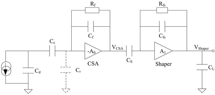
Figure 1. Proposed system structure.
In Figure 1, Cd is the junction capacitance of detector, Cr is the sum of the amplifier input capacitance and the distributed capacitance, Cc is the couple capacitance with very large value, A0 is the gain of the charge sensitive preamplifier, Cf is the feedback capacitance. Rf is used to release the signal charges accumulated on Cf, meanwhile, to provide DC negative feedback to make the circuit work in a stabile DC operating point. If the feedback capacitance Cf is equaled to the input port, the total input capacitance is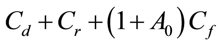 , here Cc is neglected.
If the output charge of CZT detector is Q, the voltage of signal produced in the charge sensitive preamplifier input is described as the expression (1).
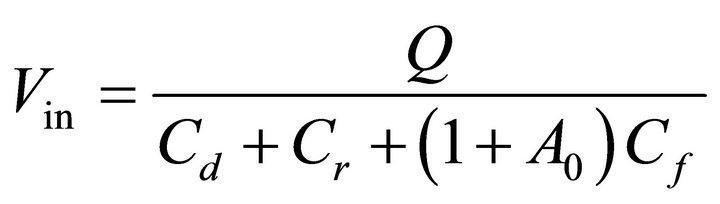 (1)
(1)
If the charge sensitive preamplifier satisfies the conditions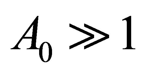 , and
, and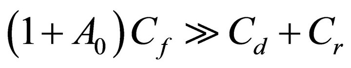 , so
, so 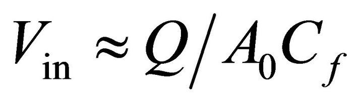 , the output voltage of preamplifier is
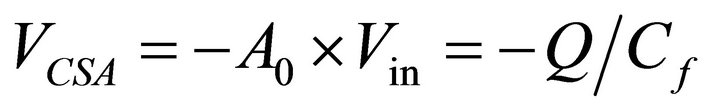 .
.
Thus, as long as the above conditions are satisfied, the output signal voltage of charge sensitive preamplifier is only proportional to the output charge amount Q of detector, and is regardless of the junction capacitance of detectors. In other words, as long as Cf is a constant value, no matter whether the Cr and A0 are stable or not, the magnification of the output voltage amplitude equated to the input charge is stable. The output voltage produced by unit charge is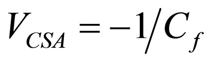 , which is called the charge sensitivity. In order to improve the charge sensitivity, we should choose a smaller Cf. So, the charge sensitive preamplifier has the abilities of low-noise and is unaffected by the stability of the junction capacitance of detector, input capacitance of the preamplifier and voltage gain. Due to these characters, the charge sensitive preamplifier has been widely used in the high-resolution spectrum measurement systems.
The signals produced by the CSA are needed to be shaped to reduce noise fatherly. The purpose of shaper is to optimize signal-noise ratio and to reduce interference between signals from different time. In frequency domain, we could consider the shaper as a band-pass filter; usually we choose second-order active CR-RC shaper. This shaper can effectively suppress the high-frequency thermal noise and low-frequency  noise, as shown in Figure 2. Therefore, we can adjust the shaper central frequency to optimize the signal-noise ratio.
Since passive resistor needs large layout area, the resistor in shaper is realized by CMOS resistor, so the resistance and also the shaping time of shaper can be adjusted to achieve the best readout signal-noise ratio.
3. Noise Analysis
This part focuses on the noise analysis of detector-preamplifier, because the noise optimization is only done in preamplifier. Figure 3 shows mainly noise sources of the detector-preamplifier. According to the locations of the noise, noise sources can be divided into two types: parallel noise sources and series noise sources.
As shown in Figure 3, ![]() and
and  are parallel noise sources, the current noise
  produced by Rf also be considered parallel with the signal current because of the low output impedance of the preamplifier. So the parallel noise sources include leakage current noise of detectors, leakage current noise of MOSs, thermal noise of feedback resistance and the equivalent resistance of detectors, as the expression (2) shown below.
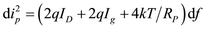 (2)
(2)
The MOS channel noise and flicker noise at the input can be equivalent to the series voltage noise , as the expression (3) shown.
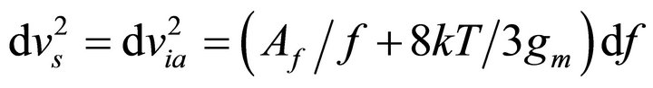 (3)
(3)
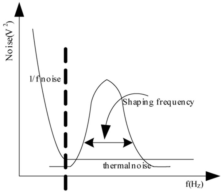
Figure 2. Shaper principle.
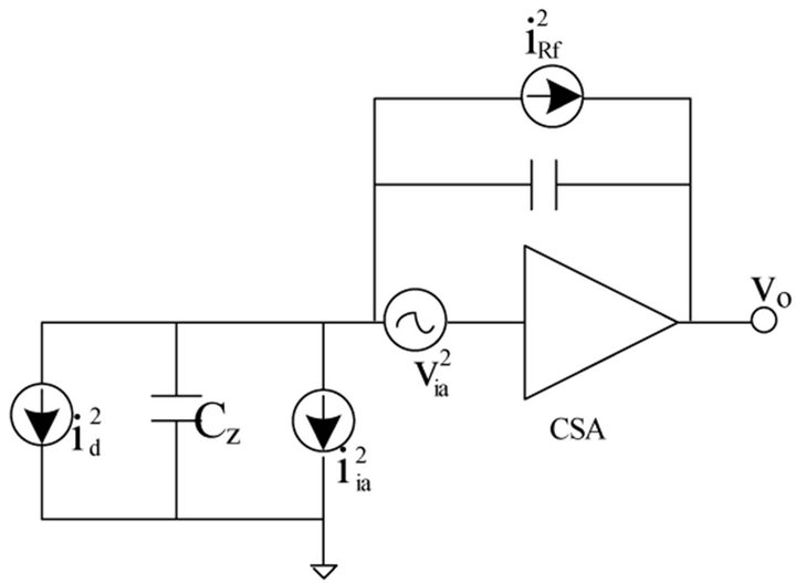
Figure 3. Signal and noise of detector-preamplifier.
Here, 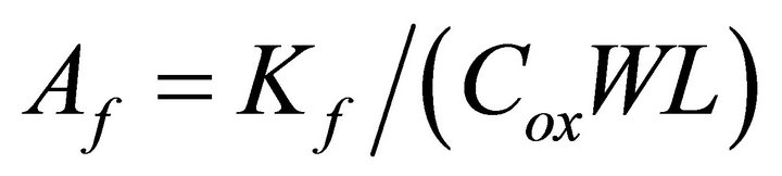 , q is unit quantity of electric charge;
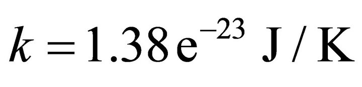 , the Boltzmann constant; gm is the transconductance of input MOS; Kf is the
  noise coefficient, related to the type of MOS and technology. In TSMC 0.35 um mixed-signal technology, PMOS:
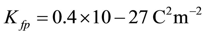 ; NMOS:
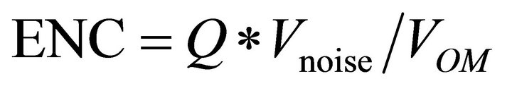
 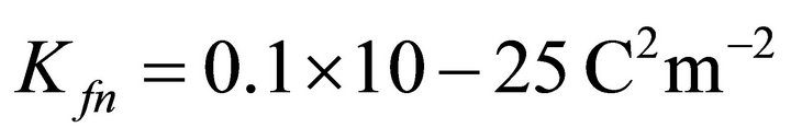 . In order to make noise as small as possible, we need to design gm larger and Kf smaller as possible. Cox is unit capacitance of MOS gate; W and L are width and length of MOS transistors. Generally, we use equivalent noise charge (ENC) to evaluate noise performance. The ENC of the whole system can be expressed as the following expression (4).
 (4)
(4)
Here, Vnoise is all the noise of the system, VOM is the amplitude of output signal; Q is the input charge amount (electronics). Usually the main consideration for the optimization of ENC is the match design of W and L of input MOS transistor [6,7].
4. Circuit and Layout Design
We can know from the noise model that all front-end readout system for radiation detectors must satisfy the requirement of low-noise. Whenever we design, we must consider the low-noise factor. And charge sensitive preamplifier-shaper must have good signal-noise ratio. In our proposed system, we can view that shaper is consisted of an ideal charge sensitive preamplifier and a capacitance. Therefore design of low-noise charge sensitive preamplifier is very important. In order to satisfy the requirements of low-noise and high-gain, this design adopts a single-end mode amplifier. Although the differential-mode amplifier can well suppress the noise, in the same conditions, the noise produced by differential-mode amplifier is 1.41 times higher than single-end amplifier because of one more input stage. So we use single-end amplifier to realize the preamplifier. The basic structure of charge sensitive preamplifier is shown in Figure 4. The input transistor is a PMOS because PMOS has lower  noise than NMOS. In order to eliminate the power noise and reduce the noise density, the source of input PMOS connects to ground. Feedback capacitance would not be MOS capacitance due to their nonlinear. Bias current source is consisted of PMOSs because by doing so not only can simplify circuits but also can reduce noise.
We design active shaper with the same base structure in Figure 4. All the simulations are done by Spectre simulator. The parameters are shown in Table 1.
Layout design is as more difficult and important part in analog integrated circuit design. Low-noise, small area, low crosstalk, low mismatch all must be taken into considering. The finally layout is shown in Figure 5.
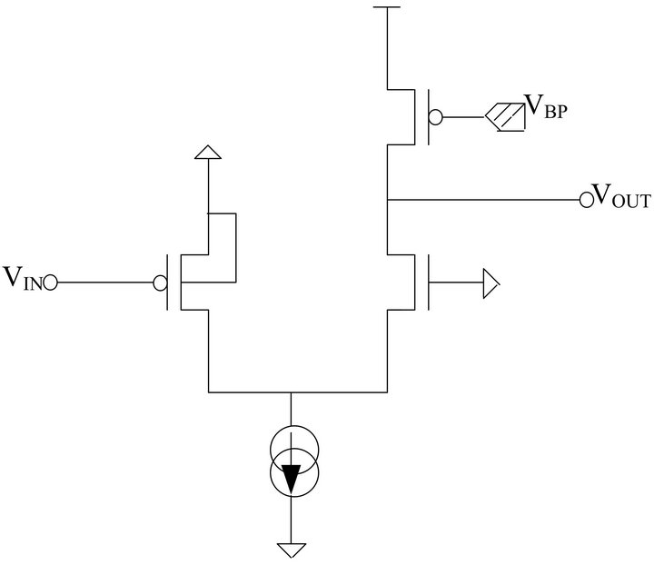
Figure 4. The base structure of charge sensitive preamplifier.
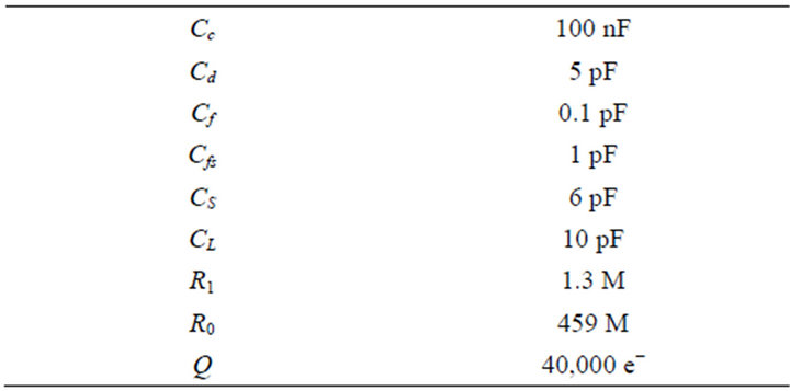
Table 1. Main parameters.
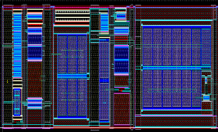
Figure 5. Layout of system.
The amount of charge Q affects signal density, in our design, the maximal input signal are 40,000 electronics. Note in Figure 6, at shaping time 1.5 us, the output amplitude is 48.2 mV at input charge of 40,000 electronics, so the gain of charge coveter to voltage is 5.8 V/pC.
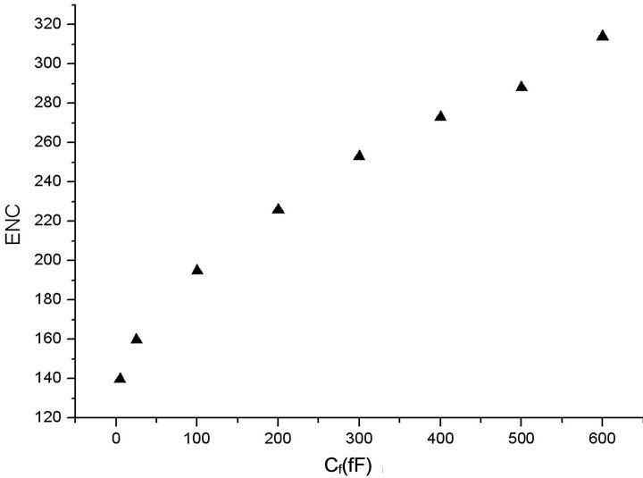
The junction capacitance of detectors, feedback capacitance, and feedback resistance would affect the system noise, so we must choose optimized values of them to make noise minimum. Figure 7 gives the results of ENC influence by feedback capacitance and feedback resistance of CSA.
Parasitical capacitance and resistance could affect the shaping time, so we would to adjust the bias voltage of
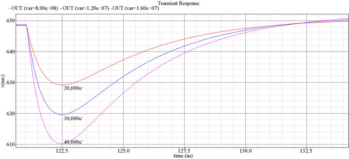
Figure 6. Output results.
 (a)
(a)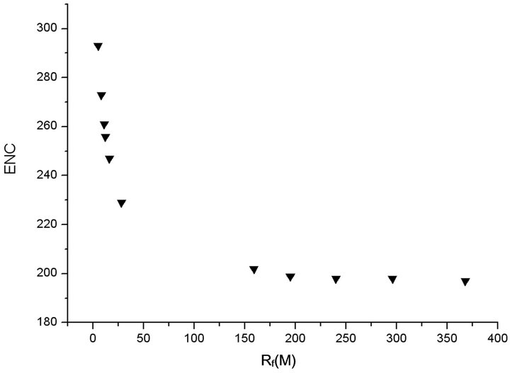 (b)
(b)
Figure 7. ENC affected by Cf (a) and Rf (b) of CSA.
feedback resistance of shaper when post-simulate. From the post simulation result, we get that the shaping time is reduced by 6% in post-simulation than pre-simulation. Figure 8 shows the system noise performance of ENC, we could view that the ENC is increased by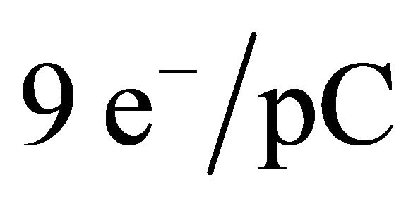 ,
, . Figure 9 shows the gain linearity of the proposed system. Through analysis, the nonlinearity of the system is <3%.
Performance summary is presented in Table 2.
In the paper, we do all work based on the proposed front-end readout system. Moreover, we also make this system as one channel of multi-channel front-end readout ASIC for CZT detectors. We design 16-channel frontend readout ASIC and finish the post-simulation. The simulation results show that the crosstalk between channels is not very good. So the next work is to do optimiza-
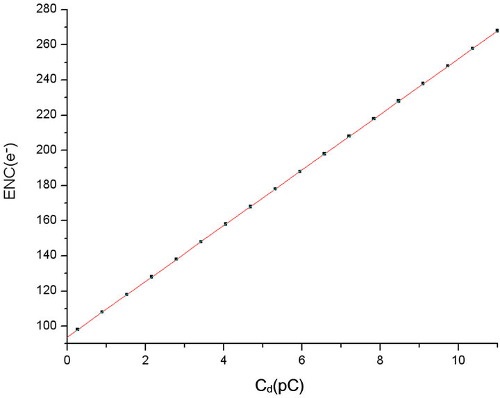
Figure 8. System noise performance of ENC (rms).
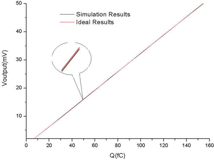
Figure 9. System gain-linearity performance.
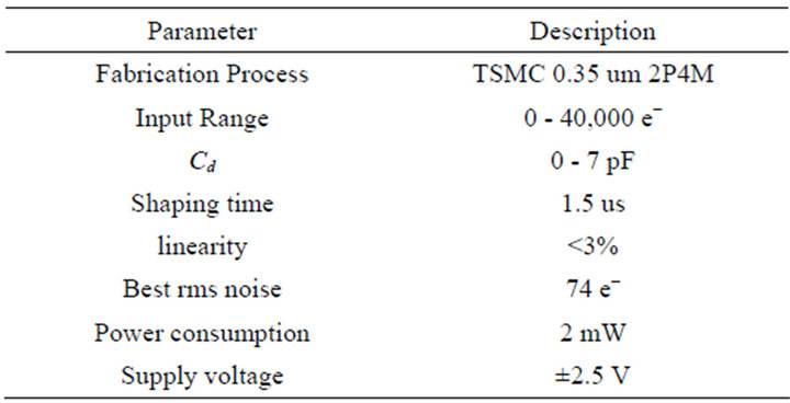
Table 2. Performance summary.
tion for multi-channelfront-end readout ASIC for CZT detectors.
5. Conclusion
In this paper, a low-noise charge sensitive preamplifier and shaper circuits are proposed for front-end readout for CZT detectors based on TSMC 0.35 um 2P4M mixedsignal fabrication process. The preliminary simulations of the system achieve a 74 e− (rms) equivalent noise charge and a 9 e−/pF noise slope with power consumption of 2 mW. The non-linearity is <3%. From the results, we note that the system can satisfy the requirement of low-noise and achieve experience for multi-channel frontend read-out ASIC for CZT detectors.
REFERENCES
- K. Iniewski and W. Davros, “Medical Imaging Principles, Detectors, and Electronics,” Medical Physics, Vol. 36, No. 11, 2009, p. 5374. doi:10.1118/1.3246610
- T. Takahashi and S. Watanabe, “Recent Progress in CdTe and CdZnTe Detectors,” IEEE Transactions on Nuclear Science, Vol. 48, No. 4, 2001, pp. 950-959. doi:10.1109/23.958705
- M. Beikahmadi and S. Mirabbasi, “A Low-Power LowNoise CMOS Charge-Sensitive Amplifier for Capacitive Detectors,” New Circuits and Systems Conference (NEWCAS), Bordeaux, August 2011, pp. 450-453.
- C. Fiorini and M. Porro, “DRAGO Chip: A Low-Noise CMOS Preamplifier Shaper for Silicon Detectors with Integrated Front-End JFET,” IEEE Transactions on Nuclear Science, Vol. 52, No. 5, 2005, pp. 1647-1653.
- T. Kishishta, H. Ikeda, T. Kiyuna, et al., “Development of a Low-Noise Analog Front-End ASIC for CdTe Detectors,” 2007 IEEE Nuclear Science Symposium Conference Record, Honolulu, 26 October 2007-3 November 2007, pp. 1992-1996. doi:10.1109/NSSMIC.2007.4436544
- Y. Hu, W. Dulinski, et al., “Design of a Low Noise, Self-Triggered, Monolithic Preamplifier Dedicated to Silicon Trackers and X-ß Imaging,” Nuclear Instruments and Methods in Physics Research A, Vol. 361, No. 3, 1995, pp. 568-573.
- Y. Hu, J. L. Solere, et al., “Design and Perdormance of a Low-Noise Low-Power Consumption CMOS Charge Amplifier for Capacitive Detectors,” IEEE Transactions on Nuclear Science, Vol. 45, No. 1, 1998, pp. 119-123.
NOTES
*This work is supported by the National Natural Science Foundation of China (No. 60972157).