Energy and Power Engineering
Vol.5 No.9(2013), Article ID:39787,10 pages DOI:10.4236/epe.2013.59061
Equal Switching Distribution Method for Multi-Level Cascaded Inverters
1Department of Electrical and Electronics Engineering, Shamoon College of Engineering, Beer Sheva, Israel
2Department of Electrical and Computer Engineering, Ben Gurion University, Beer Sheva, Israel
3Department of Computer Science, Sapir College, Sderot, Israel
Email: dmitrba@sce.ac.il
Copyright © 2013 Saad Tapuchi et al. This is an open access article distributed under the Creative Commons Attribution License, which permits unrestricted use, distribution, and reproduction in any medium, provided the original work is properly cited.
Received October 2, 2013; revised November 2, 2013; accepted November 9, 2013
Keywords: Switchings; Cascaded inverter; Multi-level; PWM
ABSTRACT
The paper proposes a new method of equal switching distribution that can be applied to cascaded multi-level inverters. This method is based on the fact that in the cascaded multilevel inverters, the output phase voltage is the sum of voltage waveforms produced by all cascaded cells. By periodically exchanging cells’ voltage waveforms, the proposed method ensures equal average switchings distribution between all cascaded cells. This method is applied to the 13-level inverter, which consists of three cascaded 5-level H-bridge cells per phase. However, the proposed method can be extended to any desired number of voltage levels and applied to any type of cascaded multi-level inverter. Extensive simulation results of the tested 13-level inverter with the equal switching distribution are presented. Moreover, the proposed method is compared to the standard control approaches and its advantages are shown.
1. Introduction
The multi-level inverter, comprising medium voltage basic cells, has entered the market of controlled voltage sources more and more due to several important advantages. They are suitable for Medium Voltage Inverters (MVI) as several active switching cells are connected in series; therefore, the multi-level inverters are suitable for high voltages high power applications. The output voltage wave is built up from several staircases that mitigate the voltage gradient dv/dt stresses on electric machine or transformer windings connected to the multi-level inverters. Furthermore, the output voltage waveform has a much lower THD factor than that of their two-level counterparts.
There are several basic configurations for multi-level inverters, and each of them has its advantages and disadvantages versus the others [1-3]. All of them produce the output voltages by adding or subtracting several distinct DC voltages to/from others. One of the configurations is the Neutral Point Clamped (NPC) multi-level inverter [4-9]. The distinct DC voltages are obtained by charging several capacitors from only one DC voltage source. The principal advantage is the need for only one DC voltage source. The principal disadvantage is the need to control and regulate the capacitor charging/discharging processes to ensure that their voltage levels remain quasi constant. Another distinct type of multi-level inverters is the Cascaded H-Bridge configuration (the multi-cell topology) [10-12]. Here, each inverter phase is built of several series connected H-bridges, while each H-bridge is supplied by its own DC voltage source. The principal advantage is stable voltage level on the H-bridge active switches which are fixed by the DC voltage sources, while their main disadvantage is the need for several DC voltage sources.
The proposed switching distribution method is applied to the 13-level inverter which consists of three series cascaded 5-level H-bridges on each inverter phase (see Figure 1). The H-bridges use a neutral point clamping approach to get 5-level phase voltages in place of the 3-level phase voltages commonly obtained with standard H-bridges. The inverter is controlled by Phase Disposition PD PWM [13,14].
The inverter 13-level output voltage per phase is obtained as a staircase wave, while each H-bridge contrib.- utes to its particular levels.
Section 2 presents the problem of H-bridge cells un-
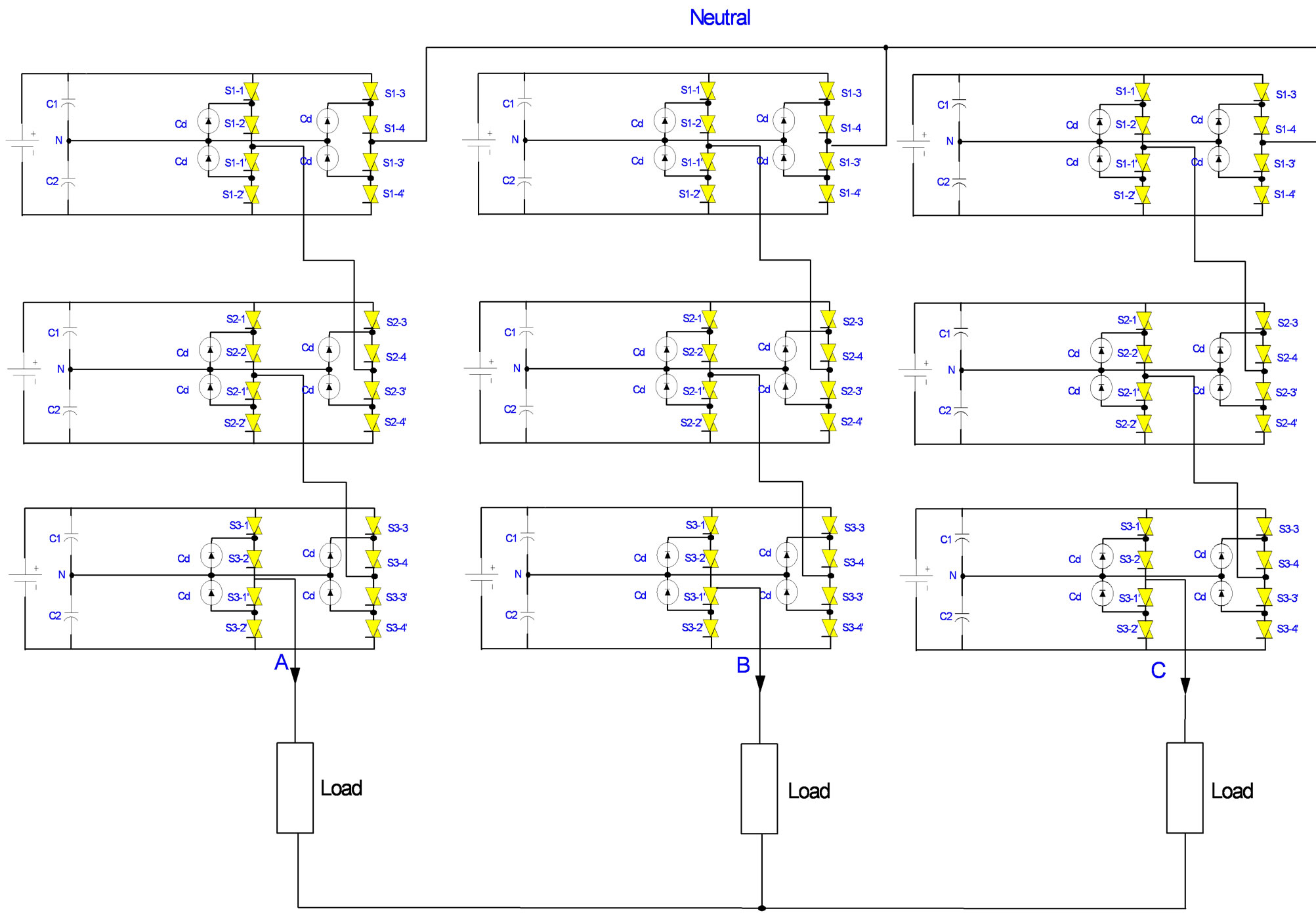
Figure 1. The proposed 13-level cascaded H-bridge inverter.
balanced loading and switching in multilevel cascaded inverters. Section 3 introduces the proposed method and the simulation results. Several aspects such as Total Harmonic Distortion Factor (THD) of the inverter output currents, phase and line to line voltages, harmonic content, frequency spectrum distribution, switching number for different modulation and carrier frequencies, and modulation indexes are simulated. Section 4 presents the conclusions of the paper.
2. The Problem of H-Bridges Unbalanced Loading and Switching in Multilevel Cascaded Inverters
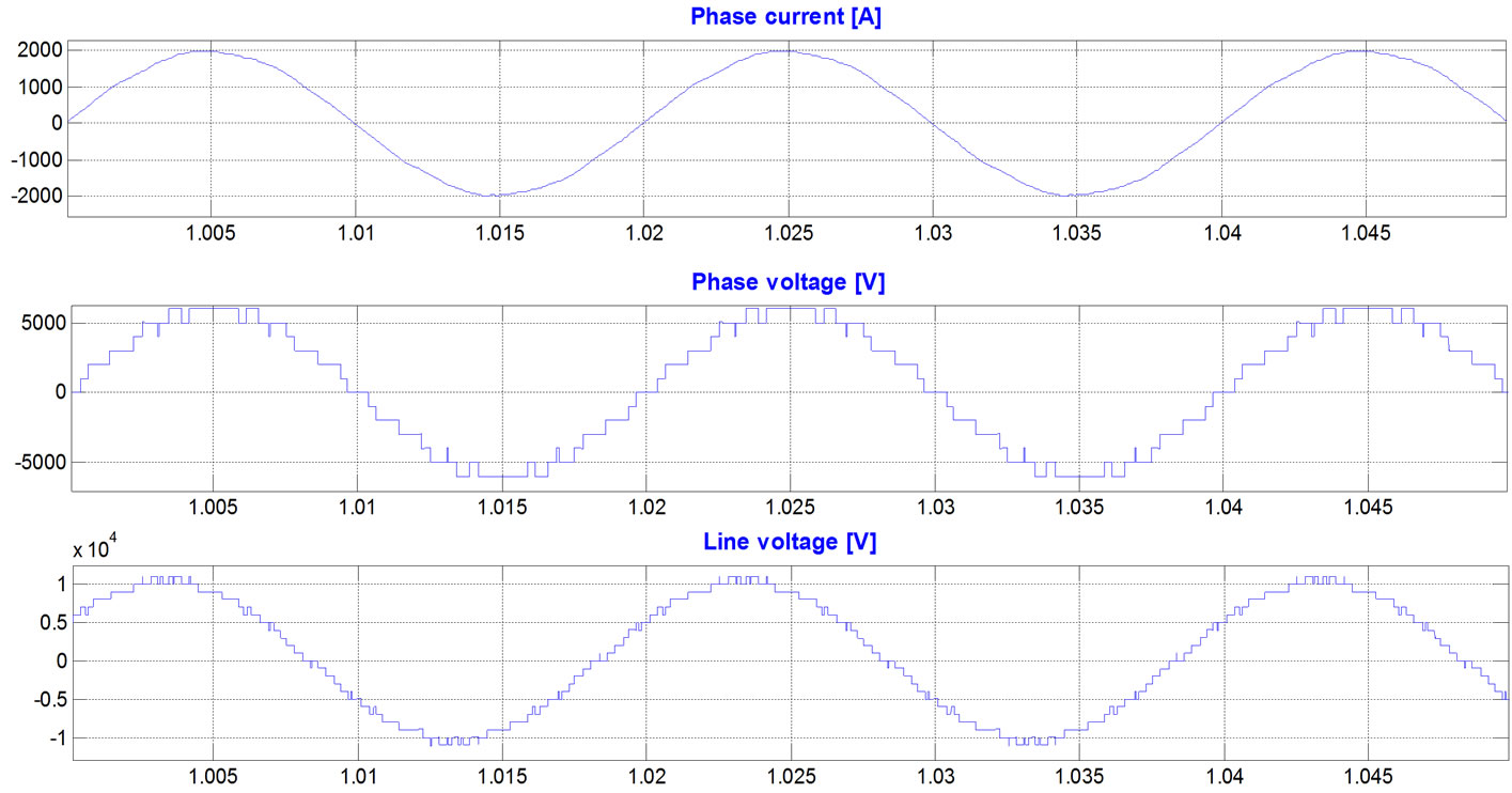
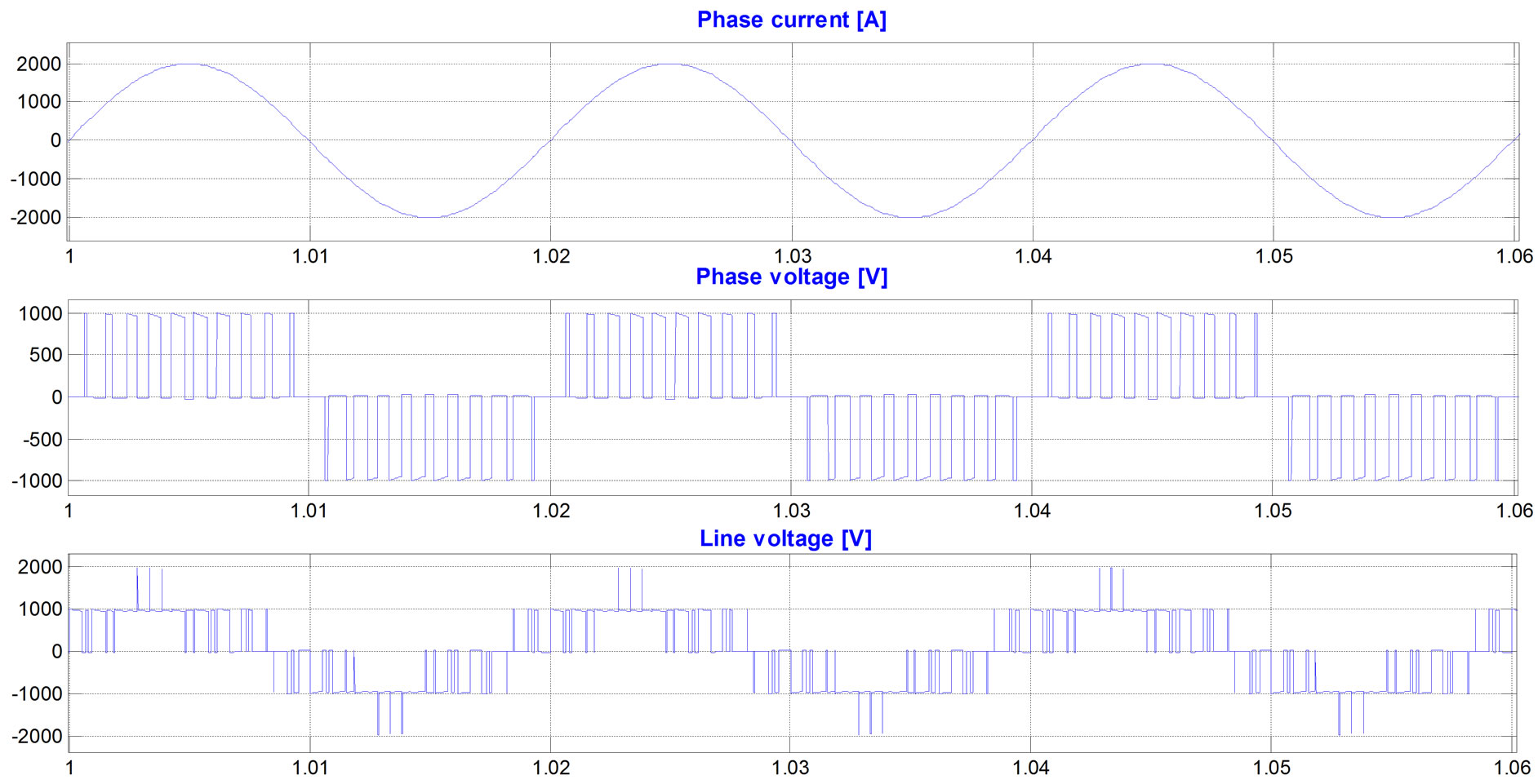
In the multi-level cascaded inverters, each H-bridge cell produces its own voltage waveform which contributes specific voltage levels to the total output phase voltage. As a result, there is a problem of unequal switching and loading of cascaded H-bridge cells. In order to understand this problem, the simulations results of 13-level cascaded inverter for modulation indexes of 1 and 0.1, with standard PD PWM control (without applying equal switching distribution method) are shown in Figure 2 and 3.
The typical loads for the inverter are synchronous motors in a quasi steady state. Therefore, a steady state model for the synchronous motor is used in simulations.The parameters of simulations are:  (per 5-level H-bridge), NPC capacitors
  mF, the load parameters per phase are:
 ,
,  H, and a sinusoidal back electro-motive force (EMF). The back EMF could be changed according to the desired power factor, frequency, and voltage.
In the case of modulation index 1, every H-bridge produces its own voltage (see Figure 2(e)) and as a result, each H-bridge has different switchings number. Table 1 shows the THDs of the phase current, phase and line voltages, and switchings number in every bridge cell. Table 1 shows that H-bridge3 has 150 switchings/sec in each transistor compared to 50 switchings/sec in Hbridge1 and H-bridge2. This unequal switching is undesirable because it can cause extra heating and shorten lifetime of the transistors in H-bridge3.
This problem becomes more severe when the modulation index is decreased below 1, especially when it approaches low values such as 0.3 and lower. When the inverter is operated at modulation index of 0.1, the phase voltage is decreased to three voltage levels (see Figure
 (a)
(a) (b)
(b)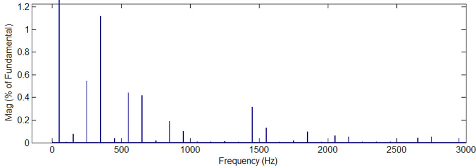 (c)
(c)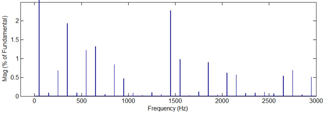 (d)
(d)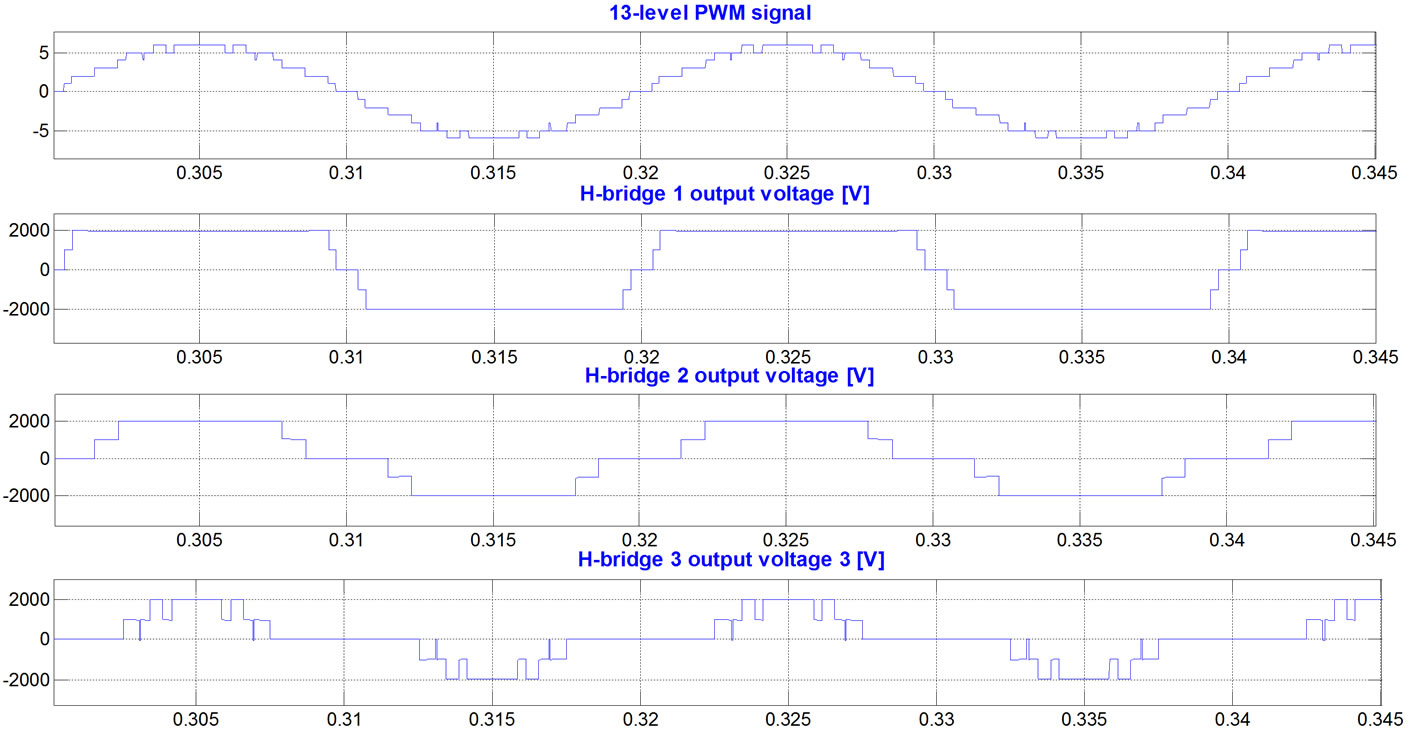 (e)
(e)
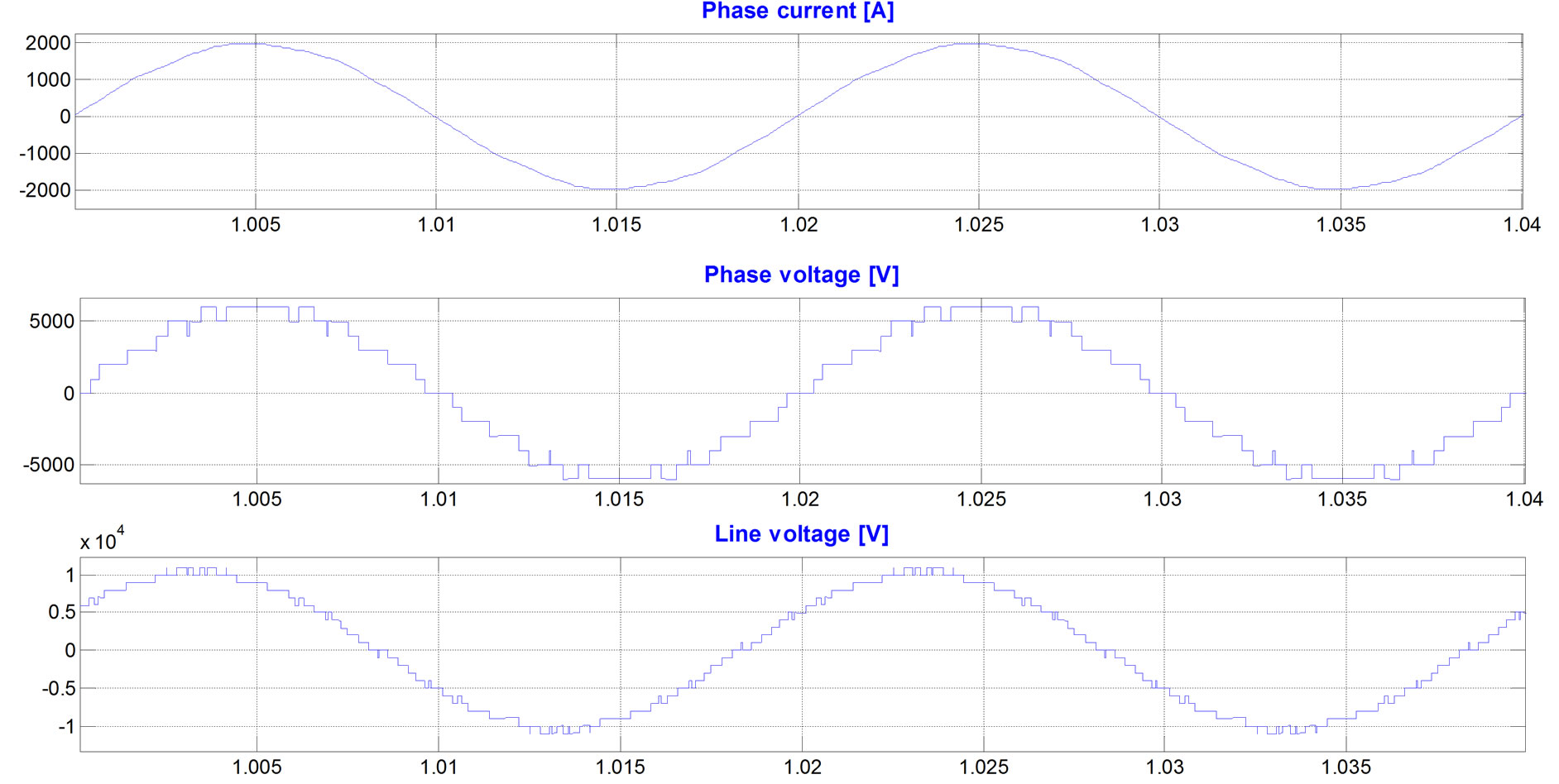
Figure 2. Simulation results, current and voltage waves and their spectra, while the modulation frequency is 50 Hz, the carrier frequency 1050 Hz, and the modulation index is 1 (there are 13 voltage levels in the output phase voltage), PD PWM method, the H-bridge cells are not exchanged: (a) phase “A” current, phase “A” voltage, and line “AB” voltage; (b) spectrum of the phase current; (c) spectrum of the phase voltage; (d)spectrum of the line voltage; (e) phase “A” 13-level PWM signal versus H-bridges output voltages.
 (a)
(a)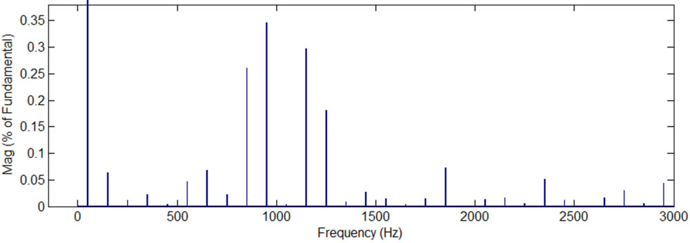 (b)
(b)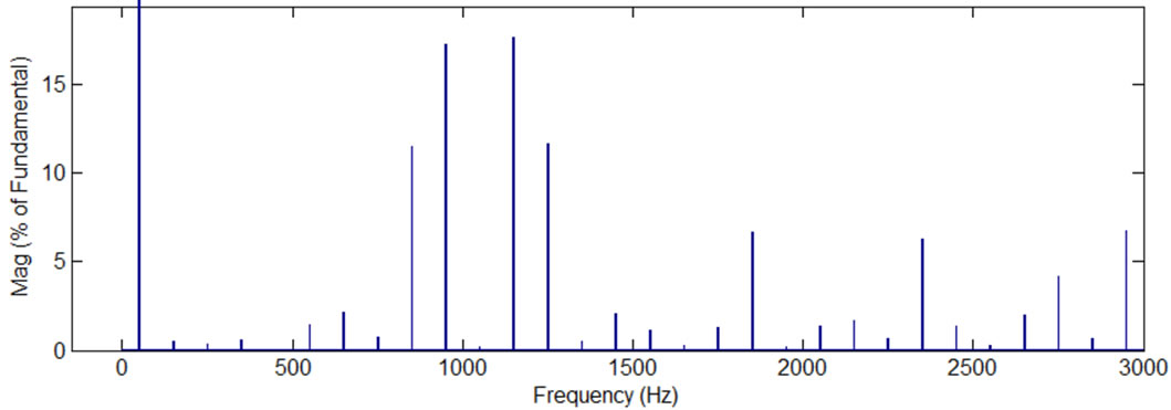 (c)
(c)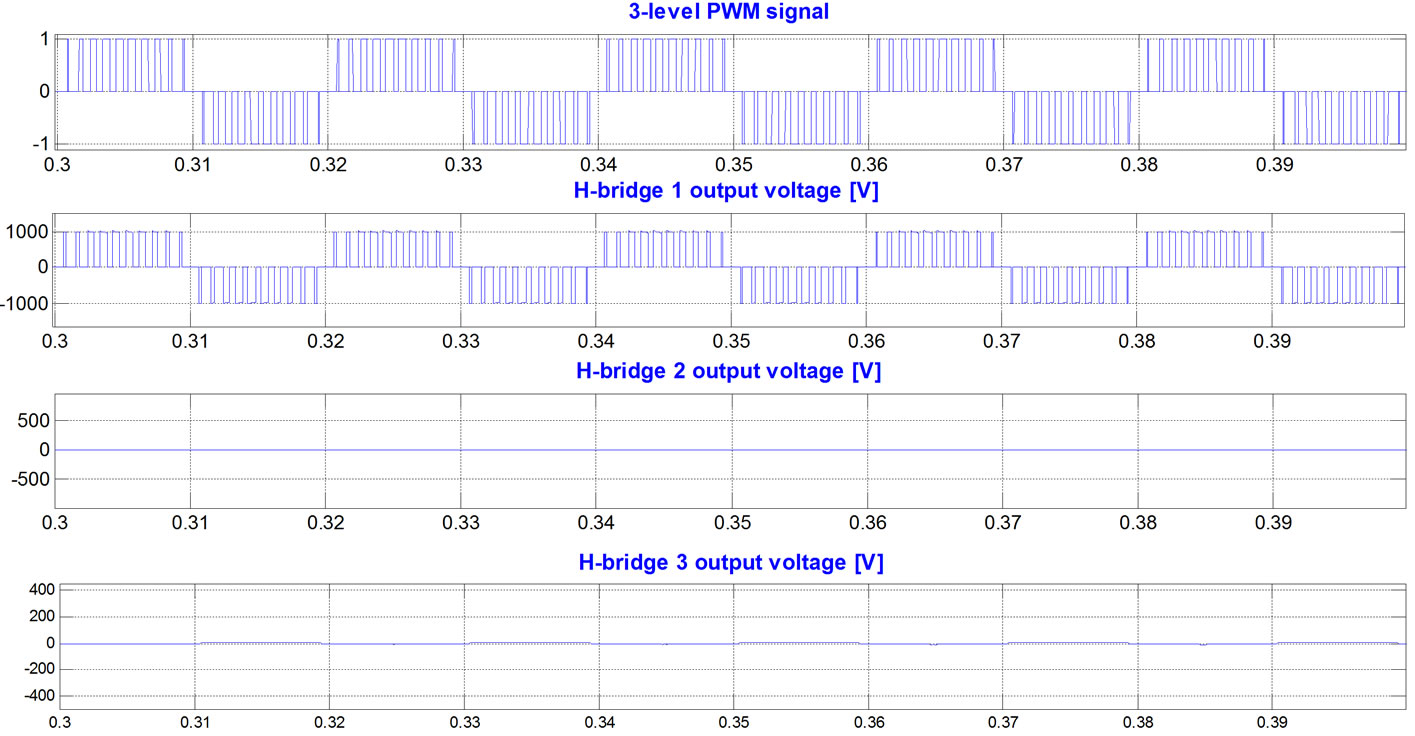 (d)
(d)
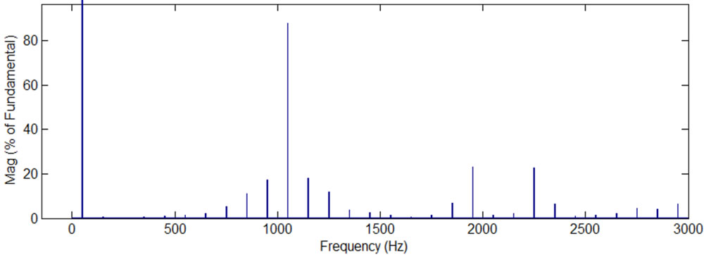
Figure 3. Simulation results, current and voltage waves and their spectra, while the modulation frequency is 50 Hz, the carrier frequency 1050 Hz, and the modulation index is 0.1 (there are 13 voltage levels in the output phase voltage), PD PWM method, the H-bridge cells are not exchanged: (a) phase “A” current, phase “A” voltage, and line “AB” voltage; (b) spectrum of the phase current; (c) spectrum of the phase voltage; (d)spectrum of the line voltage; (e) phase “A” 13-level PWM signal versus H-bridges output voltages.
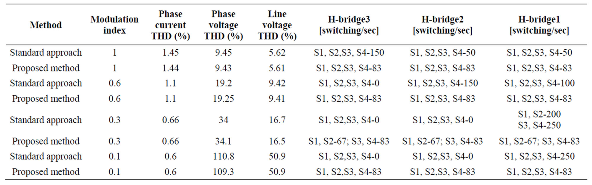
Table 1. The H-bridges switching number for different phase shift angles between the carrier and the modulation signals, modulation and carrier frequencies, modulation frequency is 50 HZ, carrier frequency is 1050 HZ, PD PWM method.
3(a)). Figure 3(e) shows that at modulation index of 0.1, only H-bridge1 is switched while the H-bridge2 and H-bridge3 are not operated at all. In this case, the H-bridge1 is switched at 250 switchings/sec in each transistor. The inverter’s operation at low modulation indexes increases imbalance in H-bridges switching and loading.
3. The Proposed Switchings Distribution Method
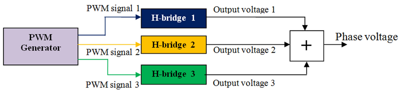
In order to solve the problem of unbalanced switching of the H-bridge cells, the equal switching distribution method is proposed. The method uses the operation princeple of the multilevel inverter: the control unit of the inverter generates the desired PWM signals that are applied to the H-bridge cells; each H-bridge cell produces its own output voltage according to the applied PWM signal. There are three H-bridges that receive three PWM signals per phase. The proposed equal switching distribution method periodically exchanges these three PWM signals between the three H-bridge cells. The exchanging of PWM signals is performed every 0.02sec, which is the cycle time of the 50Hz modulation signal. As a result, the output voltage of each H-bridge is changed three times, every 0.02sec (see Figure 4).
The phase voltage is the sum of three H-bridges output voltages. Although the output voltages are exchanged every modulation cycle, their sum remains unchanged. Therefore, the inverter phase voltages and inverter’s load are uninfluenced by the equal switching distribution method.
The proposed equal switching distribution method is applied to the 13-level cascaded inverter for modulation indexes of 1, 0.6, 0.3 and 0.1, with standard PD PWM control. Table 1 shows the comparison of 13-level cascaded inverter operated with standard approach (without application of equal switching distribution method) and operated with equal switching distribution method, for modulation indexes of 1, 0.6, 0.3 and 0.1. Moreover, the simulated phase current, phase and line voltages and H-bridges output voltages for modulation index 1 and 0.1 are shown in Figures 5 and 6 respectively.
Table 1 shows that the application of the proposed method does not affect the inverter’s load parameters such as THDs of the phase current, phase and line voltages. Moreover, the loads phase current, phase and line voltages spectrums are also unaffected by the application of the proposed method (it can be seen from comparison of Figures 2(b)-(d) with Figures 5(b)-(d) and Figures 3(b)-(d) with Figures 5(b)-(d)). This is an important advantage of the proposed method.
Figure 5(e) and Figure 6(e) show how the H-bridges output voltages are exchanged every cycle of modulation signal (0.02sec) and that average switchings number becomes equal in all three H-bridges. For example in the case of modulation index 0.1, without application of the proposed method, the transistors in H-bridge3 were switched at 250 switchings/sec and other two H-bridges were not operated at all. After application of the proposed method, transistors in all three H-bridges are switched at the same 83 switchings/sec.
Moreover, Table 1 shows that the change in the modulation index affects the number of the voltage levels in the output voltages, e.g., there are thirteen voltage levels in the phase voltage with modulation index 1, but only three voltage levels with modulation index 0.1. As a result, the appearance of the output current and voltage waves changes as well as their spectra and harmonic content and distribution. Regarding the output voltage waves, it is seen that their waves better resemble a sinusoidal wave as the number of levels increases. As a result, their THDs decrease as well. Furthermore, the harmonic content concentrates to higher harmonics as the level number decreases.
4. Conclusions
The paper presents the equal switching distribution me-
 (a)
(a)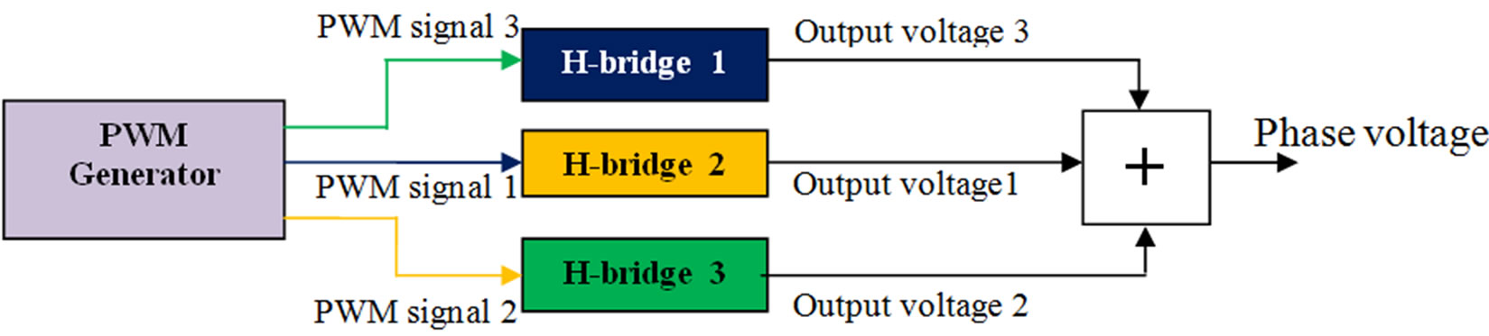 (b)
(b)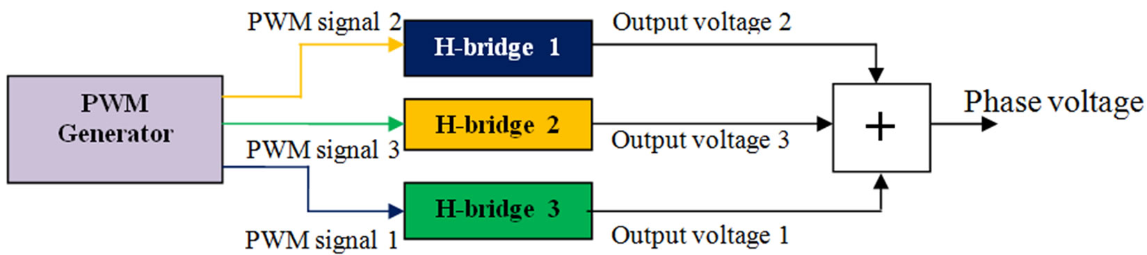 (c)
(c)
Figure 4. The PWM generator generates three PWM signals for three H-bridge cells per phase. Each H-bridge produces its output voltage according to the applied PWM signal. The obtained phase voltage is the sum of these three output voltages. The PWM signals are exchanged between the H-bridges every cycle of the modulation signal (0.02sec). After three cycles, the process is repeated; (a) the first state where PWM signal is applied to the H-bridge 1, PWM signal 2 is applied to H-bridge 2 and PWM signal 3 is applied to H-bridge 3. (b) The second state where PWM signal 3 is applied to H-bridge 1, PWM signal 1 is applied to H-bridge 2 and PWM signal 2 is applied to H-bridge 3. (c) The third state where PWM signal 2 is applied to H-bridge 1, PWM signal 3 is applied to H-bridge 2 and PWM signal 1 is applied to H-bridge 3.
 (a)
(a) (b)
(b)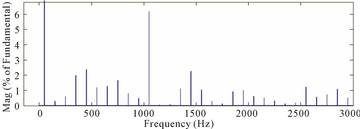 (c)
(c)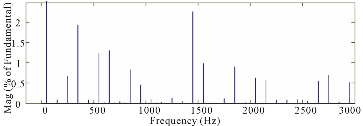 (d)
(d)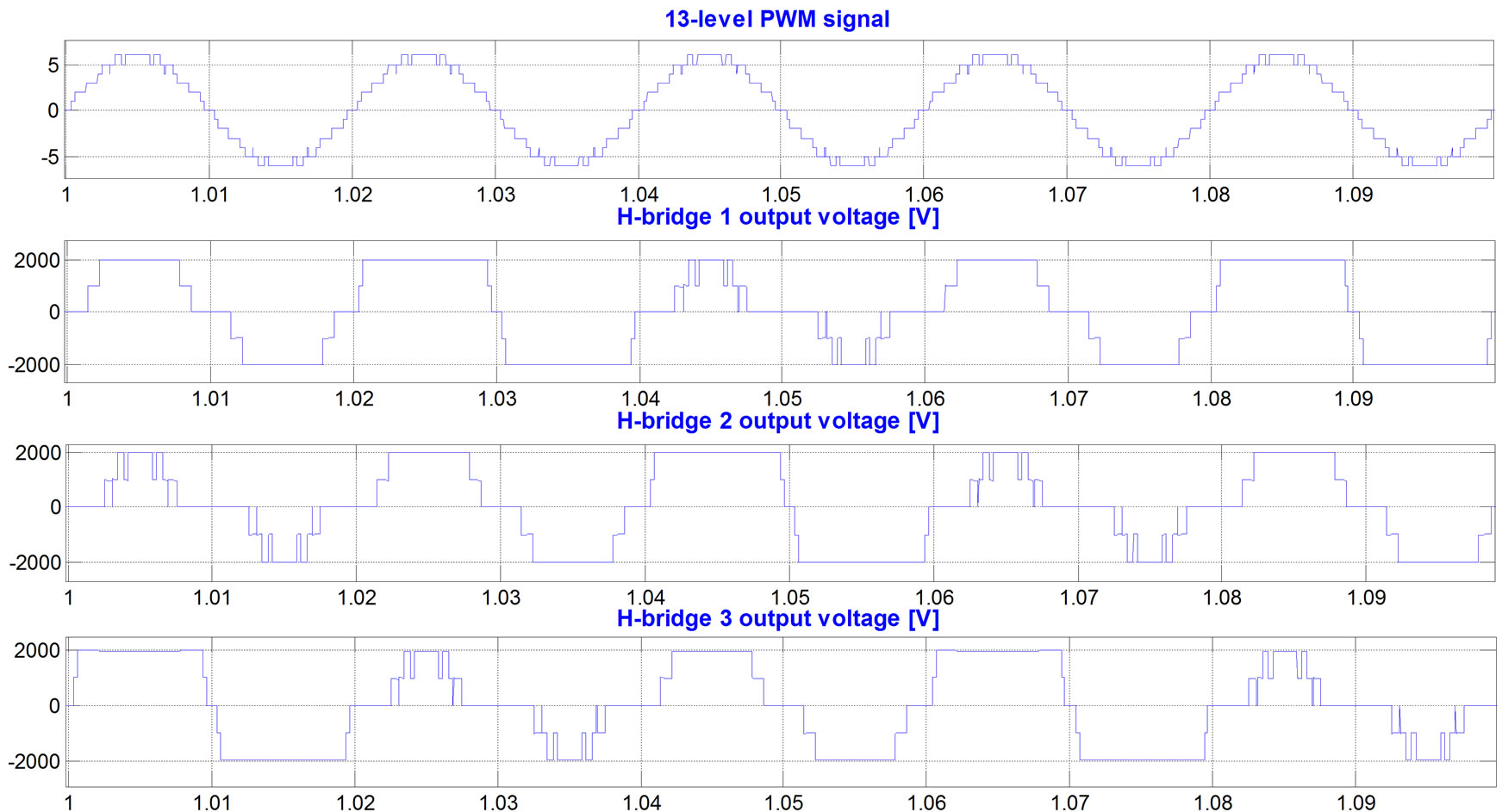 (e)
(e)
Figure 5. Simulation results, current and voltage waves and their spectra, while the modulation frequency is 50 Hz, the carrier frequency 1050 Hz, and the modulation index is 1 (there are 13 voltage levels in the output phase voltage), PD PWM method, the H-bridge cells voltages are exchanged every 0.02 sec: (a) phase “A” current, phase “A” voltage, and line “AB” voltage; (b) spectrum of the phase current; (c) spectrum of the phase voltage; (d)spectrum of the line voltage; (e) phase “A” 13-level PWM signal versus H-bridges output voltages.
 (a)
(a)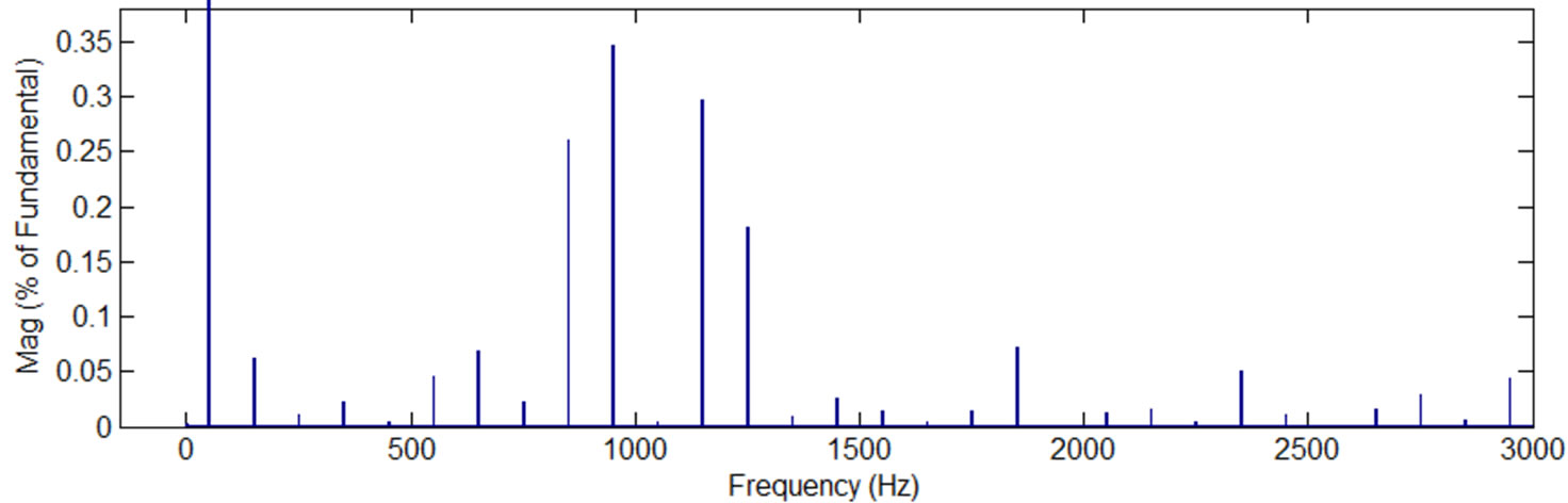 (b)
(b) (c)
(c)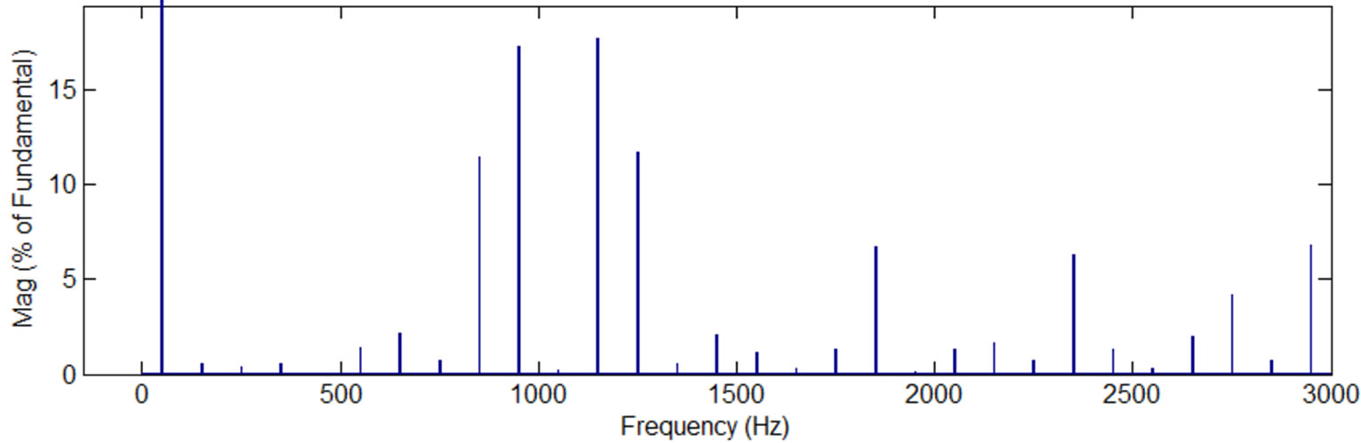 (d)
(d)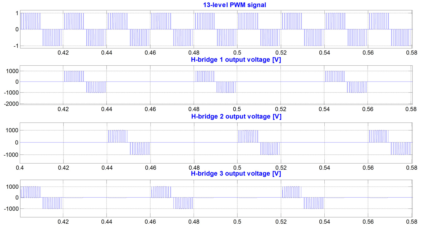 (e)
(e)
Figure 6. Simulation results, current and voltage waves and their spectra, while the modulation frequency is 50 Hz, the carrier frequency 1050 Hz, and the modulation index is 0.1 (there are 13 voltage levels in the output phase voltage), PD PWM method, the H-bridge cells voltages are exchanged every 0.02 sec: (a) phase “A” current, phase “A” voltage, and line “AB” voltage; (b) spectrum of the phase current; (c) spectrum of the phase voltage; (d)spectrum of the line voltage; (e) phase “A” 13-level PWM signal versus H-bridges output voltages.
thod for multilevel cascaded inverters. This method uses the operation principle of the multilevel inverter and periodically exchanges three PWM signals between three H-bridge cells. The exchanging of PWM signals is performed every cycle time of the 50Hz modulation signal. In order to examine the effectiveness of the proposed method, it was applied to the 13-level cascaded H-bridge inverter. However, it can be applied to any topology of cascaded multilevel inverters and to any number of levels. The tested 13-level inverter was operated by a PD carrier-based PWM approach.
The significant advantage of the proposed method is equal switching number of all H-bridge cells of the inverter. It ensures equal loading of the transistors and thus prevents their overheating and prolongs their lifetime. The total switchings number of the inverter remained unchanged. Another important advantage of the proposed method is that its application does not affect the inverter’s load parameters such as THDs of the phase current, phase and line voltages. Moreover, the loads phase current, phase and line voltages spectrums are also unaffected by the application of the proposed method.
REFERENCES
- H. Abu-Rub, J. Holtz, J. Rodriguez and G. Baoming, “Medium-Voltage Multi-Level Converters—State of the Art, Challenges, and Requirements in Industrial Applications,” IEEE Transactions on Industrial Electronics, Vol. 57, No. 8, 2010, pp. 2581-2596. http://dx.doi.org/10.1109/TIE.2010.2043039
- J. Rodríguez, S. Bernet, B. Wu, J. Pontt and S. Kouro, “Multi-Level Voltage-Source-Converter Topologies for Industrial Medium-Voltage Drives,” IEEE Transactions on Industrial Electronics, Vol. 54, No. 6, 2007, pp. 2930- 2945. http://dx.doi.org/10.1109/TIE.2007.907044
- D. Krug, S. Bernet, S. S. Fazel, K. Jalili and M. Malinowski, “Comparison of 2.3-kV Medium-Voltage Multilevel Converters for Industrial Medium-Voltage Drives,” IEEE Transactions on Industrial Electronics, Vol. 54, No. 6, 2007, pp. 2979-2992. http://dx.doi.org/10.1109/TIE.2007.906997
- J. Ewanchuk, J. Salmon and B. Vafakhah, “A Five/Nine Level Twelve Switch Neutral Point Clamped Inverter for High Speed Electric Drives,” IEEE Transactions on Industry Applications, Vol. 4, No. 4, 2011,pp. 384-392.
- B. Vafakhah, J. Ewanchuk and J. Salmon, “Multicarrier Interleaved PWM Strategies for a Five Level NPC Inverter Using a Three Phase Coupled Inductor,” IEEE Transactions on Industry Applications, Vol. 47, No. 6, 2011, pp. 2549-2558. http://dx.doi.org/10.1109/TIA.2011.2168931
- Z. Rech and C. Pinheiro, “Comparison of Neutral-PointClamped, Symmetrical, and Hybrid Asymmetrical Multilevel Inverters,” IEEE Transactions on Industrial Electronics, Vol. 57, 2010, pp. 2297-2306. http://dx.doi.org/10.1109/TIE.2010.2040561
- J. Rodriguez, S. Bernet, P. K. Steimer and I. E. Lizama, “A Survey on Neutral Point Clamped Inverters,” IEEE Transactions on Industrial Electronics, Vol. 57, No. 7, 2010, pp. 2219-2230. http://dx.doi.org/10.1109/TIE.2009.2032430
- D. Baimel, S. Tapuchi and R. Rabinovici, “Novel Multilevel Hybrid Cascaded Inverter for High Power Motion Control Systems,” Applied Mechanics and Materials, Vol. 432, 2013, pp. 345-350. http://dx.doi.org/10.4028/www.scientific.net/AMM.432.345
- D. Baimel and S. Tapuchi, “A New Topology of FiveLevel Neutral Point Clamped Inverter for Motion Control Systems,” Applied Mechanics and Materials, Vol. 432, 2013, pp. 336-340. http://dx.doi.org/10.4028/www.scientific.net/AMM.432.336
- M. Malinowski, K. Gopakumar, J. Rodriguez and M. Pérez, “A Survey on Cascaded Multilevel Inverters,” IEEE Transactions on Industrial Electronics, Vol. 57, No. 7, 2010, pp. 2197-2206. http://dx.doi.org/10.1109/TIE.2009.2030767
- G. Waltrich and I. Barbi, “Three Phase Cascaded Multilevel Inverter Using Power Cells With Two Inverter Legs in Series,” IEEE Transactions on Industrial Electronics, Vol. 57, No. 8, 2010, pp. 2605-2612. http://dx.doi.org/10.1109/TIE.2010.2043040
- P. Cortés, A. Wilson, S. Kouro, J. Rodriguez and H. Abu-Rub, “Model Predictive Control of Multilevel Cascaded H-bridge Inverters,” IEEE Transactions on Industrial Electronics, Vol. 57, No. 8, 2010, pp. 2691-2699. http://dx.doi.org/10.1109/TIE.2011.2158773
- B. Cougo, G. Gateau, T. Meynard, M. Bobrowska-Rafal and M. Cousineau, “PD Modulation Scheme for Three Phase Parallel Multilevel Inverters,” IEEE Transactions on Industrial Electronics, Vol. 59, No. 2, 2012, pp. 941- 949.
- D. Holmes and T. Lipo, “Carrier Based PWM of Multilevel Inverters,” Pulse Width Modulation of Power Converter Principles and Practice EBook, 2003, pp. 453-530.