Open Journal of Applied Sciences
Vol.4 No.3(2014), Article ID:43622,5 pages DOI:10.4236/ojapps.2014.43014
Analytical Evaluation of Energy and Electron Concentrations in Quantum Wells of the High Electron Mobility Transistors
Salih Saygi
Department of Physics, Faculty of Arts and Sciences, Gaziosmanpasa University, Tokat, Turkey
Email: ssaygi20@yahoo.com
Copyright © 2014 by author and Scientific Research Publishing Inc.
This work is licensed under the Creative Commons Attribution International License (CC BY).
http://creativecommons.org/licenses/by/4.0/


Received 9 January 2014; revised 15 February 2014; accepted 23 February 2014
ABSTRACT
In this letter we propose analytical evaluation method for the electron density and the energy density in multi-layered high electron mobility transistors (HEMTs). The algorithm is used to simulate the variation of the electron density and the energy density against temperature of heterojunction AlGaN/GaN. The proposed procedure guaranties the reliable application of the contribution of multi-layered HEMTs structure. In conclusion, the obtained results are estimated and discussed.
Keywords:HEMT; Semiconductors; Electron Density; Energy Density; Binomial Coefficient

1. Introduction
Mathematical modeling plays an important role in design and manufacture of the semiconductor devices. In other words, the modeling of such devices can solve countered problems. The Metal Semiconductor Field Effect Transistors and the High Electron Mobility Transistors can be used as microwave oscillators, switches, attenuators and amplifiers intended for ultra-high speed discrete circuit elements [1] -[3] . This kind of devices can also be incorporated into monolithic integrated circuit in modern technology. The requirement for high power and high frequency involves transistor devices based on semiconductor materials with both large breakdown voltage and the high electron velocity. Two advantageous of devices can be counted. One is the presence of wide bandgap, which leads to high breakdown voltages and high saturation velocity. Second it is the existence of many heterostructure with high conduction band-offset and high piezoelectricity, which results high sheet carrier densities [3] [4] .
The ability of GaN to form heterojunction makes it superior compared to other nitride semiconductors. A typical such device consists of ternary semiconductor layers with different proportion of mole fraction of aluminum.
A heterojunction device is shown in Figure 1. In the layer’s interface the electrons are kept in thin potential well and the scattering progresses of electrons are insignificant, therefore the fast operation occurs.
The conventional devices progressed with metallic pads may require either a precise etching control for the gate recess or heavy doping for the junction gate. Therefore they should show a problem of small transconductance due to a large parasitic resistance. Recently, to construct these multilayer devices, some specific processes have presented. As can be understood, the design and constructing of such devices are not easy. It requires very remarkable growth for optimization. To help understand the operational mechanisms of these structures and to optimize their design various modeling methods have been developed [5] -[8] . Trading with the current continuity and energy transport equations a covering method with special functions has been given by Cole and Snowden [9] . The counting of the Schrödinger equation adds considerably difficulties to the solutions and numerical routines. Further modification factors were also added to the numerical routines by Cole [10] .
As the aim of the present, the corrected accurate analytical method established in Ref. [11] has been applied to realistic the GaN based multilayer device to optimize their design. Therefore it is going to be shown that the instant mathematical and numerical modeling engages an important role in picturing the corresponding energy and electron densities for such structures.
2. Definitions and Calculations Formulas
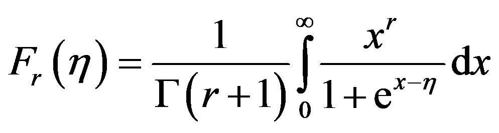
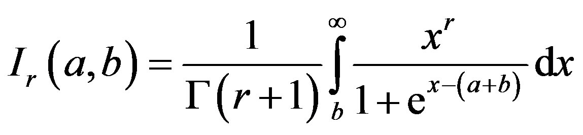
In Cole’s approximation, the estimated formulas for the energies and electron concentrations reduces to  functions.
  functions are replacement of the Fermi integrals. Therefore to evaluate the
  functions more accurate than what existing methods have, a contribution can be arranged for analytical expression
  and be easily implemented with an algebraic computer language. In the Refs. [8] [9] , the authors have presented a well-defined theoretical framework of approximation for multilayered High Electron Mobility Transistors (HEMTs). Further, an efficient analytical approach has been recently given by Mamedov [12] .
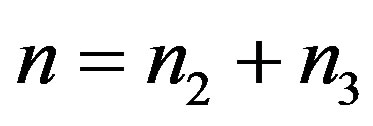
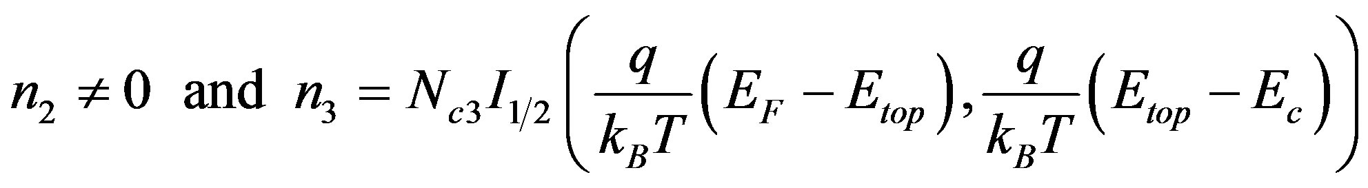
The total electron density is given by
 , (1)
, (1)
as Cole suggested,  for the “two-dimensional” electrons is the contribution from the subbands given by the solution of the Schrödinger Equation and
  for the “three-dimensional” electrons is the bulk electron density. In Equation (1) the quantities are defined as, respectively, for outside the potential well
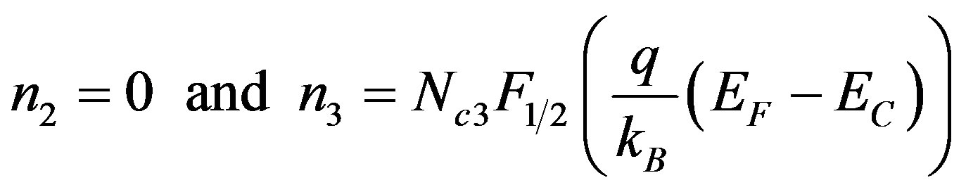 , (2)
, (2)
for inside the potential well
 . (3)
. (3)
Also the corresponding expressions for the energy density in full non-degenerate case are defined by for outside the quantum wells
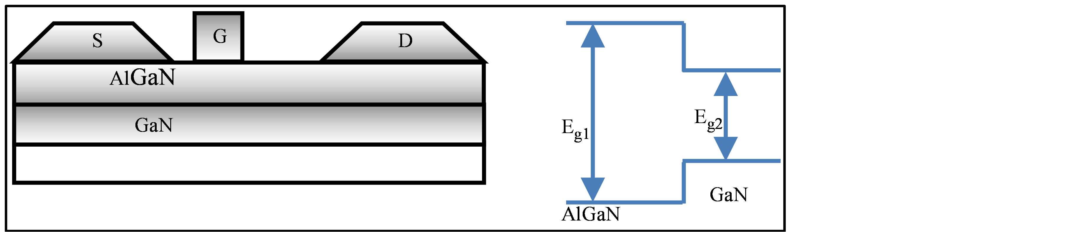
Figure 1. AlGaN/GaN HFET device structure and the band offset of different layers.
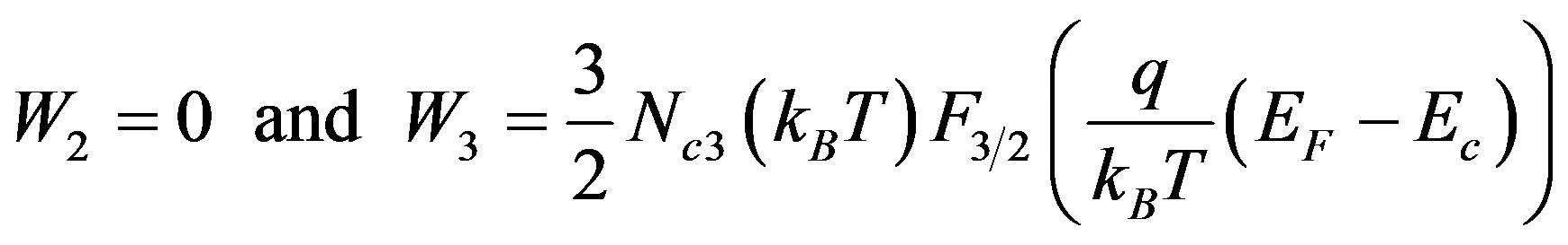 , (4)
, (4)
for inside the quantum wells
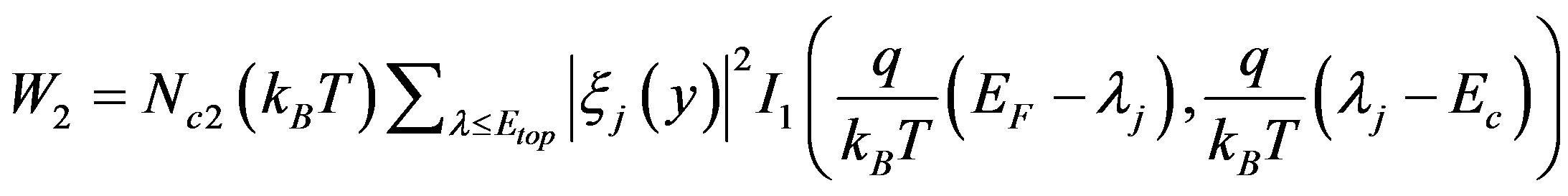 (5)
(5)
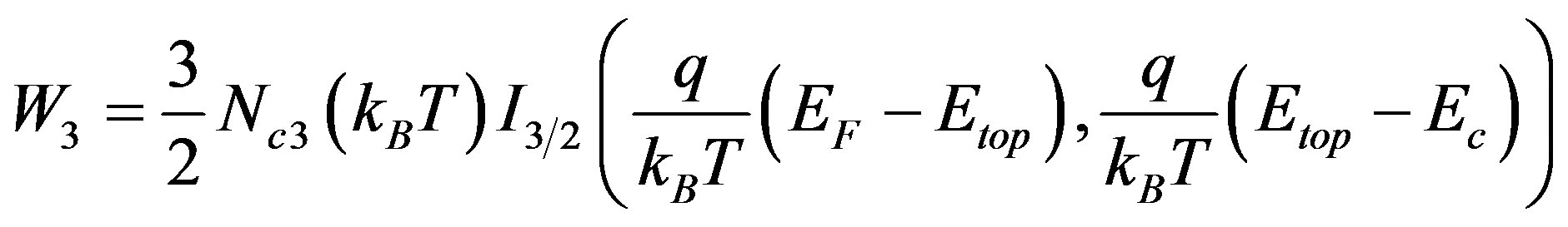 (6)
(6)
where the electron concentration and the electron effective mass is depicted like
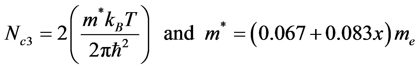 .
.
It can be seen from Equations (2)-(6), the formulas for electron density and energy density in a HEMTs device reduced to 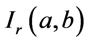 and
and  Fermi functions. The definition
  and
and 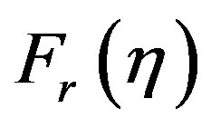 functions are given in the following form, respectively
 (7)
(7)
 . (8)
. (8)
In Ref. [11] the integrals 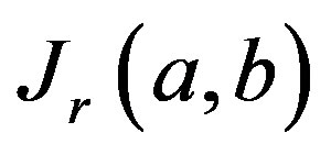 and
and  have been given following simply structured formulas, respectively
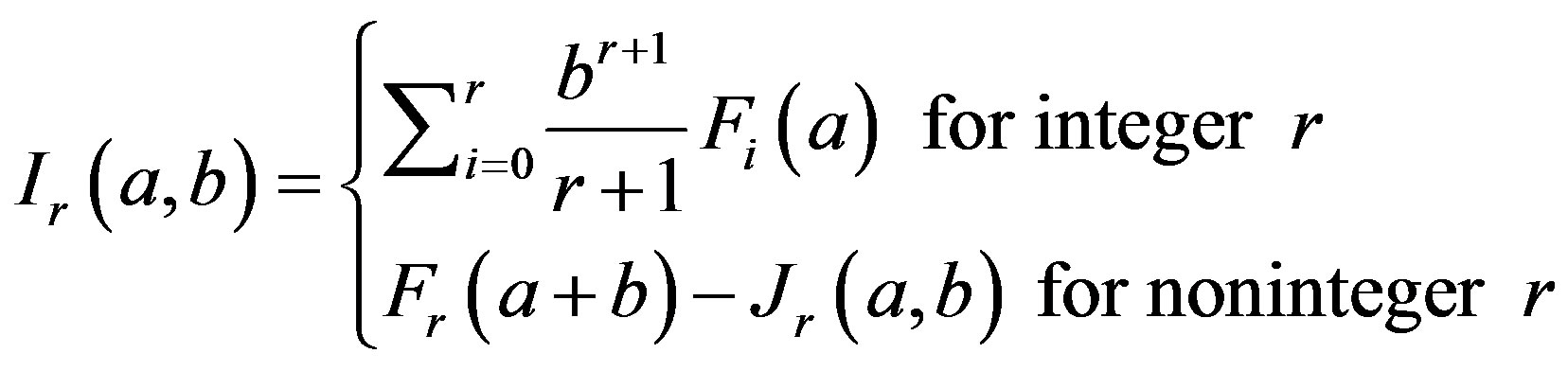 (9)
(9)
 (10)
(10)
where the quantities  have determined by the relation
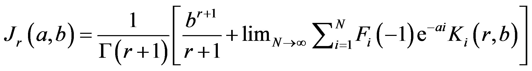 (11)
(11)
See Refs. [13] [14] for exact definitions of functions 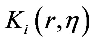 and
and .
.
3. Applications and Discussions
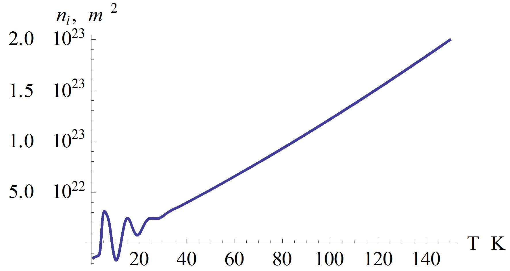
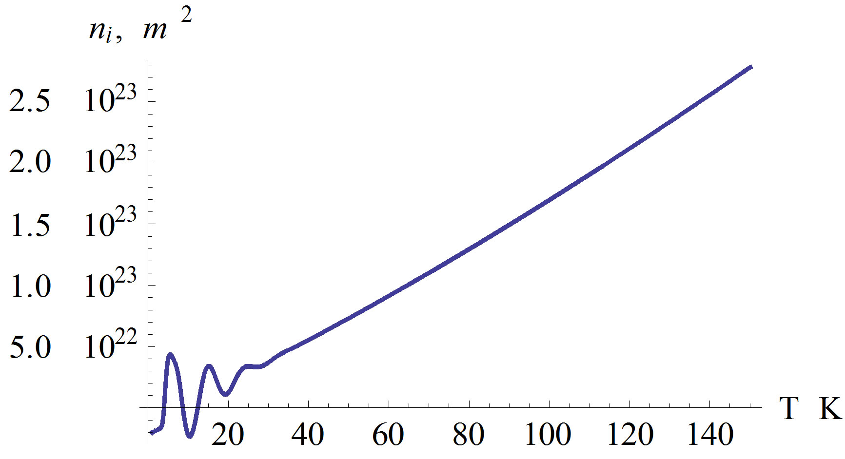
To demonstrate the reliability of the method, the proposed formulas have been firstly implemented in existing electron and energy density of the AlGaN/GaN based HEMT devices. The variation of the electron and energy densities for inside and outside layers of the structure AlGaN/GaN against temperature are shown in Figures 2 and 3.
The implementation of different layers of HEMT device pursues that when Al content goes to zero, the energy and electron concentration values for GaN layer are found. Otherwise, dealing some nonzero values of Al content gives the energy and electron concentration values for AlGaN layer.
Linear behavior of distributions demonstrates that used theoretical approximation yields sufficiently accuracy for the values of alloy’s parameters. Figures 2 and 3 depict that the electron and energy concentrations are linearly increase for the temperature values of 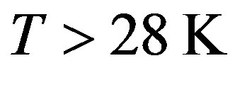 in the AlGaN/GaN based devices. As seen from Figures 2 and 3, the electron and energy concentration are altering harmonically in the temperature range
 . We
. We
 (a)
(a)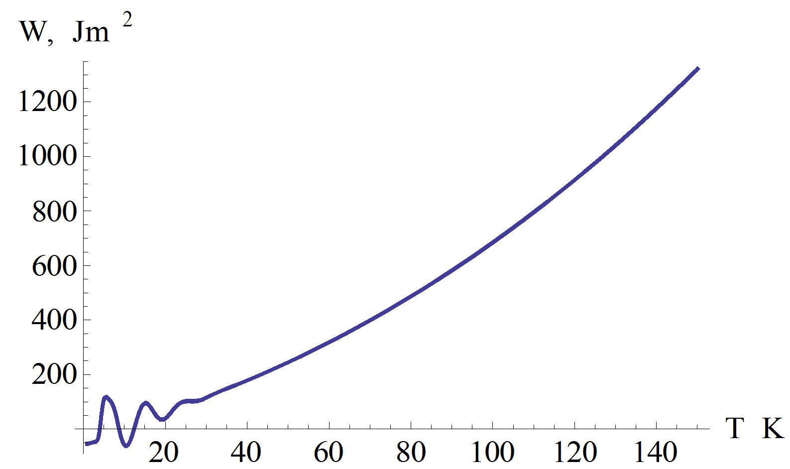 (b)
(b)
Figure 2. Temperature dependent of energy density and electron density for AlGaN/GaN structure, Al content .
.
 (a)
(a)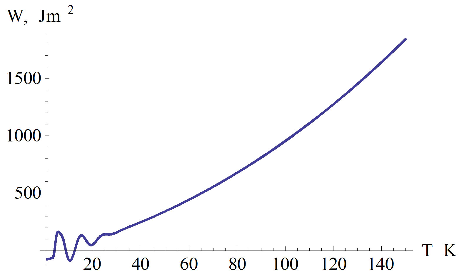 (b)
(b)
Figure 3. Temperature dependent of energy density and electron density for AlGaN/GaN structure Al content .
.
should evaluate this circumstance as following. The average value of electron and energy concentrations in semiconductor heterojunctions has not changed at the temperature range . It is understood that the electrons are in a harmonically oscillating behavior in the temperature range
 . As far as we know, there are no theoretical studies on the evaluation of semiconductor heterojunction in this temperature range. Therefore, it is an important theoretical result of our study. Also we speculate that, the temperature value
  can be concluded as a changing point of electron and energy concentration of semiconductor heterojunctions.
The work is in progress for the theoretical calculation of the temperature dependence of the energy and electron concentrations of AlGaN/GaN structured HEMT devices. Note that the characteristics given above of the heterojunctions with other semiconductor categories can be investigated with the same manner.
References
- Khan, M.A., Chen, Q., Yang, J.W., Shur, M., Dermott, B.T. and Higgins, J.A. (1996) Microwave Operation of GaN/ AlGaN-Doped Channel Heterostructure Field Effect Transistors. IEEE Electron Device Letters, 17, 1. http://dx.doi.org/10.1109/55.506356
- Simin, G., Hu, X., Ilinskaya, N., Kumar, A., Koudymov, A., Zhang, J., Khan, M.A., Gaska, R. and Shur, M.S. (2000) 7.5 kW/mm2 Current Switch Using AlGaN/GaN Metal-Oxide-Semiconductor Heterostructure Field Effect Transistors on SiC Substrates. Electronics Letters, 36, 24. http://dx.doi.org/10.1049/el:20001401
- Khan, M.A., Hu, X., Simin, G., Lunev, A., Yang, J., Gaska, R. and Shur, M.S. (2000) AlGaN/GaN Metal Oxide Semiconductor Heterostructure Field Effect Transistor. IEEE Electron Device Letter, 21, 2. http://dx.doi.org/10.1109/55.821668
- Saygi, S., Koudymov, A., Adivarahan, V., Yang, J., Simin, G., Khan, M.A., Deng, J., Gaska, R. and Shur, M.S. (2005) Real-Space Electron Transfer in III-Nitride Metal-Oxide-Semiconductor-Heterojunction Structures. Applied Physics Letters, 87, 43505. http://dx.doi.org/10.1063/1.2001745
- Adachi, S. (1985) GaAs, AlAs, and AlxGa1−xAs B: Material Parameters for Use in Research and Device Applications. Journal of Applied Physics, 58, R1-R29. http://dx.doi.org/10.1063/1.336070
- Akhtar, A.I., Guo, C.Z. and Xu, J.M. (1993) Effect of Well Coupling on the Optical Gain of Multi Quantum-Well Lasers. Journal of Applied Physics, 73, 4579. http://dx.doi.org/10.1063/1.352774
- Tang, T.W. (1984) Extension of the Scharfetter-Gummel Algorithm to the Energy Balance Equation. IEEE Transactions on Electron Devices, 31, 1912. http://dx.doi.org/10.1109/T-ED.1984.21813
- Snowden, C.M. and Miles, R.E. (1993) Compound Semiconductor Device Modeling, Springer, New York. http://dx.doi.org/10.1007/978-1-4471-2048-3
- Cole, E.A.B. and Snowden, C.M. (1995) Numerical Algorithms for Modelling Microwave Semiconductor Devices. International Journal of Numerical Modelling: Electronic Networks, Devices and Fields, 8, 13. http://dx.doi.org/10.1002/jnm.1660080104
- Cole, E.A.B., Boettcheryz, T. and Snowden, C.M. (1997) Corrections to the Calculation of Bulk Electron Densities in Quantum Wells of HEMT. Semiconductor Science and Technology, 12, 100. http://dx.doi.org/10.1088/0268-1242/12/1/018
- Cole, E.A.B. (2001) Integral Evaluation in the Mathematical and Numerical Modeling of High-Electron-Mobility Transistors. Journal of Physics: Condensed Matter, 13, 515. http://dx.doi.org/10.1088/0953-8984/13/3/311
- Mamedov, B.A. (2008) Accurate Evaluation of Integrals Arising from the Bulk Electron Densities in Quantum Wells of High Electron Mobility Transistor. Computer Physics Communications, 178, 673. http://dx.doi.org/10.1016/j.cpc.2008.01.001
- Guseinov, I.I. and Mamedov, B.A. (2004) Evaluation of Incomplete Gamma Functions Using Downward Recursion and Analytical Relations. Journal of Mathematical Chemistry, 36, 341. http://dx.doi.org/10.1023/B:JOMC.0000044521.18885.d3
- Gradsteyn, I.S. and Ryzhik, I.M. (1980) Tables of Integrals, Series and Products. Academic Press, New York.