Advances in Materials Physics and Chemistry
Vol.06 No.07(2016), Article ID:68283,9 pages
10.4236/ampc.2016.67021
Conductive Behavior and Morphology of Axially Modified Gallium Phthalocyanine Thin Films onto Indium Tin Oxide Substrates
Margarita Rivera1, Brenda Reyes1, María Elena Sánchez-Vergara2*, Luis Humberto Mendoza-Huizar3
1Instituto de Física, Departamento de Materia Condensada, Universidad Nacional Autónoma de México, D.F. México, México
2Facultad de Ingeniería, Universidad Anáhuac México Norte, Huixquilucan, Estado de México, México
3Centro de Investigaciones Químicas, Mineral de la Reforma, Universidad Autónoma del Estado de Hidalgo, Hidalgo, México

Copyright © 2016 by authors and Scientific Research Publishing Inc.
This work is licensed under the Creative Commons Attribution International License (CC BY).
http://creativecommons.org/licenses/by/4.0/


Received 9 June 2016; accepted 10 July 2016; published 13 July 2016
ABSTRACT
Semiconductor molecular films based on a gallium phthalocyanine chloride (GaPcCl) and a bidentate amine were prepared by using vacuum thermal evaporation and electrochemical techniques in order to investigate the preferred conduction paths within the films. Scanning Electron Microscopy (SEM) and Atomic Force Microscopy (AFM) were employed to characterize the morphology of the films. The conductivity measurements were performed with two different methods in order to investigate preferential conduction directions. The film transverse conductivity was obtained by using scanning tunneling spectroscopy (STS) and the in-plane film conductivity was measured with a four-point probe system. From spectroscopy measurements, the tunneling conductance (dI/dV) was also obtained. From these results, it was found that the conductive nature of the films was strongly influenced by the deposition technique which in turn defined the morphological characteristics of the film. The evaporated method showed better conductivity response and provided semiconductor characteristics in the film transverse direction with an in-plane ohmic response. Finally, contact angle measurements were performed and showed hydrophobic characteristics in all cases.
Keywords:
Thin Films, Phthalocyanines, Electronic Properties, Electrical Conductivity

1. Introduction
Metal phthalocyanines (MPcs) are very stable pi-conjugated macrocyclic aromatic compounds coordinated to metal elements that show high chemical and thermal stability and a very strong optical absorption in the visible region [1] . For several years now, metal phthalocyanine molecules have been employed as organic compounds for many high-technology applications such as photoconductivity, non-linear optics, catalysis, chemical sensors and photovoltaic cells, among others [1] [2] . It is well known that modifications on the MPc by introducing peripheral substituents and axial ligands can strongly influence and finally tune the solubility, photocatalytic, electrochemical, optical, conductive, etc. properties of the MPcs complexes [1] - [4] . The axial substitution produces relevant changes on the electronic structure of the molecule, in particular the pi-electronic distribution, as a consequence of changes in the spin density and dipole moment of the central metal-axial ligand bonds [5] .
In terms of the central metal ion, nowadays there are over seventy different MPc complexes, all exhibiting diverse physical and chemical properties as a result of the intrinsic properties of the metal core [6] . In addition, many of the central metal elements on the macrocycle ring have at least one site that can be coordinated to different ligands. Most of the MPcs found in literature correspond to transition metal complexes, but little work has been done to investigate the other metals in the periodic table. In particular, gallium phthalocyanines (GaPcs) have exhibited interesting non-linear optic (NLO) and optical limit (OL) properties that can be used to prepare optical limit materials [7] - [9] . In order to produce suitable materials for optical applications, gallium phthalocyanines complexes have been deposited as thin films by using spin-coating [10] [11] and vacuum sublimation [8] [12] [13] techniques. It is well known that the deposition technique strongly influences the molecular aggregation and orientation within the film, which in turn modifies most of the properties of the dye layer. Although several studies have been devoted to investigating physical and chemical properties of electrodeposited metal phthalocyanines such as LiPc [14] , CuPc [15] , MnPc [16] and FePc [17] , among others; up to our knowledge, no work has been done to produce GaPcs films by using electrodeposition methods in order to investigate the influence of the metal ion, the oxidation state, the electrolytic bath composition and the ligands in the structural properties of the films, among others [18] - [21] . Also, it is worth mentioning that in addition to the previous aspects, electrodeposition has become a very interesting film formation technique since the thickness of the films can be accurately controlled to produce very thin layers by controlling the electrochemical parameters.
So, in this work, the formation of thin films from gallium phthalocyanine molecules axially coordinated to a 1,4-diaminobutane molecule (1,4-LGaPc) was performed by using two different deposition techniques (electrodeposition and vacuum thermal evaporation). The 1,4-diaminobutane molecule is a simple polyamine with no optical response in the visible range, but with biological activity that can be explored in the design of biological sensors. On the other hand, indium tin oxide (ITO) substrates were employed since they are widely used as transparent conductive surfaces in electronic devices, and also, they also exhibit interesting semiconductor properties which can be directly associated to the carrier transport at surfaces or interfaces for technological applications. Since GaPcs exhibit interesting optical properties in contrast with the polyamine system, the aim of this project was to study the morphological, optical and conductive properties of the films in terms of the deposition technique by using different microscopy techniques, UV-vis spectroscopy, the four-point probe and scanning tunneling spectroscopy methods, respectively. Finally, since different applications depend on the conduction paths within the film, the conductivity characteristics along the perpendicular and parallel direction with respect to the substrate for these films are also investigated in terms of the deposition technique.
2. Materials and Methods
2.1. Synthesis
All the reactants employed were acquired from commercial suppliers and were used with no further purification. A solution of the GaPcCl (C32H16ClGaN8) in absolute methanol was added to a solution of the 1,4-diaminobu- tane (C4H12N2) in the same solvent. The 1,4-LGaPc molecule was synthesized by a simple anion exchange reaction. 0.20 g (0.3 mmol) of C32H16ClGaN8 in 25 ml absolute methanol was added to 0.40 g (4.5 mmol) of C4H12N2 previously dissolved in 25 ml of absolute methanol. The resulting solution was refluxed for three days until a blue precipitate appeared. The solid was filtered off, washed with absolute methanol and dried in vacuum. The product was recrystallized in a 1:1 methanol-water solution. Yield 77%. m.p. 350˚C (dec). Calculated analysis for C36H27N10Ga: C, 64.57%, N, 20.92%, H, 4.04%. IR (cm−1) nmax: 3424, 3212 cm−1 (N-H), 3061, 1160, 749 cm−1 (CH), 1628 cm−1 (C-C), 685 cm−1 (C-C), 1282, 1160, 1079 cm−1 (C-N) [17] [22] . FT-IR measurements were obtained with a spectrophotometer Nicolet iS5-FT using KBr pellets. Fast atomic bombardment (FAB+) mass spectroscopy of the powder samples was performed on a 3-nitrobenzyl alcohol support in the positive ion mode on a Jeol spectrometer, model JMS-SX102A.
2.2. Film Deposition
As deposition surfaces, Nanocs ITO films onto glass substrates of 100 ohms/square were employed. The substrates were ultrasonically clean at room temperature, dried under a nitrogen flux and store under vacuum prior to deposition. The film formation was carried out by using vacuum thermal evaporation and electrodeposition methods onto ITO substrates. In the first case, the substrate temperature was kept at 298˚K during deposition. In order to achieve high purity thin films, a vacuum chamber was used with a diffusion pump, together with a special molybdenum crucible with a double-grid cover. The temperature through the boat was selected in order to prevent thermal decomposition of the compound. The pressure in the vacuum chamber before the film deposition was 1 × 10⁻⁵ torr. For the film electrodeposition, a BAS potentiostat Epsilon model with a BAS 100/W electrochemical analyzer interface was employed. Tetrabutylammonium was used as support electrolyte in a 12:1 molar ratio, since it has been successfully used in the formation of conductive polymers [23] and the electrochemical deposition of a CoPc film [24] . In this work, ITO substrates were used a working electrodes, Ag/AgCl as reference electrodes and a platinum wire as counter electrode. In order to determine the potential window for the 32schronoamperometric deposition, a cyclic voltammetry experiment between the cathodic (−2.0 V) and anodic (+2.0 V) switching potentials was performed. The final reduction potential for this complex started at −0.545 V and ended at −1.200 V towards the anodic region, since it produced a similar film thickness with respect to the evaporation method in order to compare both film properties.
2.3. Film Characterization
The surface morphology and the chemical composition of the electrodeposited films were investigated with a scanning electron microscope (SEM) JEOL JSM5600 LV. The AFM morphological characterization of the films was performed ex situ by using the tapping mode in a JEOL JSPM 4210 microscope. The roughness values were obtained after analyzing the AFM images with the JEOLW inspm Processing software. The conductivity measurements were performed with two different methods in order to investigate preferential conduction directions. Film transverse conductivity and spectroscopy plots were obtained by using a JEOL JSM4210 scanning tunneling microscope with mechanical cut Pt/Ir tips. For these curves, average measurements were obtained. At least eight different sites of each film were probe measuring 16 different IV plots in each site. The tunneling conditions were +1 V, 1 nA, where electrons tunnel from filled states of the tip into empty states of the sample. Film in-plane conductivity measurements were performed with a four-point probe head couple to a 2400 Keithley source/meter. In a similar way as in the previous case, average measurements are reported. Finally, contact angle measurements were performed with a Pocket Goniometer PG3 model instrument and ultrapure (Milli-Q) water in order to investigate the films wettability characteristics. For these results, average values from three different sites with four different measurements each are reported.
3. Results and Discussion
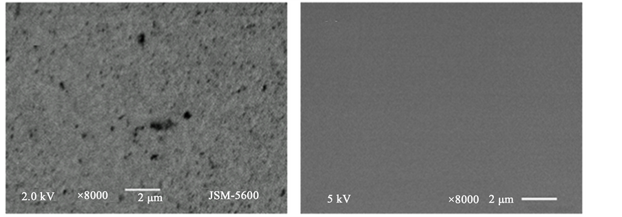
In Figure 1, the chronoamperometric plot for a 32 s electro deposition time at −1.200 V reduction potential is shown. From this curve, a characteristics mass-transfer-limited controlled mechanism can be seen. In Figure 2, scanning electron microscopy images of the films are shown at 8000×. The electrodeposited film obtained from the −1.200 V reduction potentials showed a homogenous film although the surface coverage is not uniform. Defects as pores can be appreciated along the surface as seen in Figure 2(a). The shape of the pores is irregular
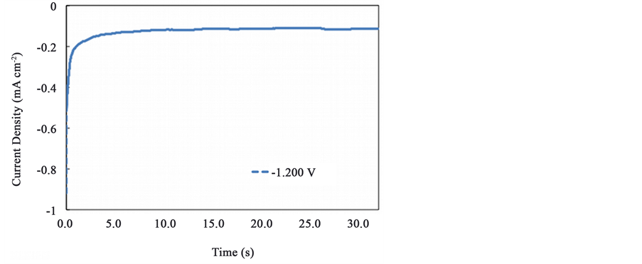
Figure 1. Chronoamperometric plot of the 1,4-GaPc film deposition onto ITO substrates.
 (a) (b)
Figure 2. Scanning electron microscopy images of the films at 8000×.
and their sizes vary from 0.1 um to 1.6 um. In Figure 2(b), the film obtained with the evaporation method showed the highest uniformity and best coverage in contrast with the other deposition technique.
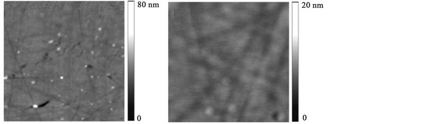
A closer inspection of the surface morphology of the films was performed with an AFM microscope. In Figure 3 , the surface characteristics can be seen. Images are 5 × 5 μm. From these figures, the −1.200 V electrodeposited film (Figure 3(a)) shows an interface with pores and grains in agreement with the SEM image. In Figure 3(b), the film showed in general a very compact structure although some linear defects attributed to the substrate can be observed. From the z-scale AFM bars, it can clearly be seen that the best film in terms of homogeneity and surface coverage corresponded to the evaporated method. Moreover, the roughness values for each film are 1.2 nm and 0.5 nm, respectively, in agreement with the SEM results. The average thickness of the films was 55 nm.
As it was mentioned previously, the conductivity measurements were performed in two different directions, perpendicular and along the film surface in order to investigate preferential conduction paths. In Figure 4, the averaged I-V plots for the electrodeposited and evaporated films are shown. From this image, the evaporated film shows the typical trend of an n-type semiconductor around 0 V bias. A small asymmetric band-gap by the zero conductance region showing a higher current at positive bias, suggests the presence of a small Schottky barrier. In contrast, the electrodeposited film exhibits a roughly linear conductivity trend in the −1.0, +1.0 interval and around the zero bias voltage suggesting an ohmic behavior.
On the other hand, in order to further investigate the electronic properties of the films, the tunneling conductance (dI/dV) was plot. It is well know that the dI/dV value corresponds to the local electron density of states and can give some information on the nature of the electrical conductivity within the film. In Figure 5, the dI/dV
 (a) (b)
Figure 3. AFM tapping mode images of the (a) electrodeposited at −1.200 V and (b) vacuum thermal evaporated film surfaces. Images are 5 μm × 5 μm.
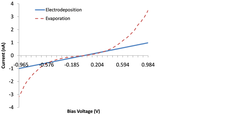
Figure 4. Scanning tunneling spectroscopy I-V plot for the electrodeposited and evaporated films in the −1 V, +1 V bias voltage interval.
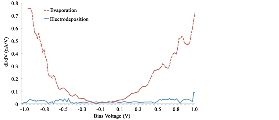
Figure 5. Conductance curves (dI/dV) for the molecular films onto ITO. No data smoothing was applied.
plot for each of the films was plotted for comparison. It is worth mentioning that these measurements were performed at room temperature in air in contrast to typical UHV experiments [25] , so we focus the analysis in terms of the shape of the band gap, in the (−1, +1) V interval and around zero bias where no net tunnel current flows across the junction. From the evaporated curve, a slightly asymmetric U shape around the Fermi level was identified, which corresponds to a typical semiconductor structure In contrast, the −1.200 V electrodeposited film shows a semi-flat plot along the interval, showing a very limited constant current flow. Both curves show noise features due to the acquisition under ambient conditions which are irrelevant in this case for the conductivity comparison.
From the dI/dV plots and considering the thickness of the films, no peak related features associated to the molecules are observed, but only the molecular related HOMO and LUMO bands. Moreover, from Figure 5, a HOMO/LUMO shift towards negative sample bias as well as a small narrowing of the band gap for the evaporated plot is observed, possible due to the film thickness. By measuring the distance between the onset regions at the HOMO/LUMO zones, a band gap of 1.1 eV was obtained. From the dI/dV electrodeposited film plot, a zero conductance is observed in the +1, −1 bias voltage interval. These results can be understood in terms of the film quality. From the SEM images, it is clear that pores were formed in the electrodeposited film. From the characteristics of the pores, they seem to go deep towards the ITO substrate and therefore, defects as voids perpendicular to the film plane can be inferred. These irregularities affect the charge transport in that direction, and therefore, show a lack of transverse conductivity. On the other hand, because of the high homogeneity of the evaporated film, the perpendicular conductivity suggests a semiconductor-like behavior. Another aspect to consider is the absence of important peaks in the limited voltage range (±1.0 V) employed. The small oscillations in the plots are most probably due to mechanical or thermal noise, since the measurements were acquired at ambient conditions. Nevertheless, the shape of the dI/dV plots is well defined and it shows a semiconductor behavior for the evaporated film and a non-conductive response for the electrodeposited layer in the perpendicular direction of the film.
By using the four-point probe method, the in-plane conductivity of the film was measured. In Figure 6, the I-V plots that represent the conductivity of the films obtained by the different deposition methods are shown. From this image, the evaporated film showed higher resistance in contrast with the −1.200 V electrodeposited film. The resistance for the evaporated sample was one order of magnitude lower in contrast with the film obtained with the electrodeposited method; that is, 0.34 ohms cm and 8.62 ohms cm, respectively. It is important to mention that the previous results were normalized and the contribution of the bare ITO substrate was removed in order to better appreciate the intrinsic resistivity values of the films. From these results, it is clear a lower resistance is found for the charge carriers of the evaporated film in the in-plane direction in contrasts with the electrodeposited one. It has been noticed that the molecular orientation and the molecular overlap of the molecules within films and heterojunctions, affect significantly the charge transfer, and therefore, the quantum efficiency of photovoltaic devices. In addition, most photovoltaic arrangements required a charge transfer efficiency to be optimum in the perpendicular direction to the substrate, so the charge carriers can travel from the anode to the cathode of the system. So, in particular for organic devices, the donor film must exhibit a semiconductor behavior so the energy band gaps can couple with the energy levels of the other organics layers to improve the charge mobility. On the other hand, the situation is different for organic films used as sensor devices. In order to have an optimum absorption, the detector surface area must be high in order to capture the largest possible amount of analytes, which is optimum along the film parallel to the substrate plane. Since a large conductivity value is required for this application, a conductor behavior is required in this direction. From our results, it was found that the evaporated film exhibits a semiconductor behavior perpendicular to the substrate and the electrodeposited film shows a better charge mobility along the in-plane direction. So it is clear that the deposition technique profoundly affects the conduction direction, and therefore, must be selected with caution when selecting the film formation technique.
Finally, the wetting properties of the films were studied since this parameter can be important for the subsequent deposition of more films or the interaction of the films with the surrounding environment for practical applications. The contact angle images are shown in Figure 7.
From these images, both films showed hydrophobic nature with contact angles of 98.5 ± 0.8 and 101.2 ± 0.9 for the electrodeposited and evaporated films, respectively. This result was expected since both, the GaPc molecule and also the 1,4-diaminobutane molecule, exhibit hydrophobic characteristics, although the difference among both deposition techniques is very small. It is worth mentioning that a wettability study of vacuum evaporated Copper phthalocyanine films onto glass substrates showed hydrophilic properties [26] , which suggest
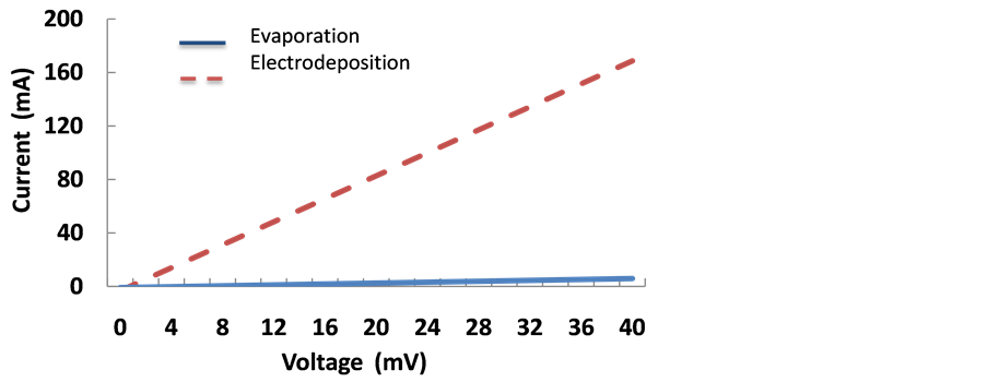
Figure 6. Four-point probe I-V plots of the electrodeposited and evaporated films.
 (a) (b)
Figure 7. Contact angle images of the (a) electrodeposited at −1.200 V and (b) vacuum thermal evaporated films.
that not only axially coordinated ligands, but also the type of central metal atom, can affect the surface energy of the film.
4. Conclusions
Molecular films from GaPcCl axially modified with the 1,4-diaminobutane molecule were synthesized and characterized. The gallium phthalocyanine films were deposited by using two different methods, vacuum thermal evaporation and electrodeposition onto ITO substrates. The information obtained from the absorption spectra indicates that these films absorb light on both sides of the blue-green region. The evaporated films showed better morphological characteristics with very high homogeneity and low roughness value in comparison with the electrodeposited films. The contact angle measurements showed hydrophobic surfaces in both cases.
From the conductivity behavior, the evaporated film showed in the perpendicular direction a semiconductor behavior and an ohmic resistivity along the in-plane film. In contrast, the electrodeposited film, exhibited insulator characteristics through the film in the perpendicular direction and high resistance in the in-plane orientation. These results can be attributed to the molecular overlap among the molecules within the film as a result of the presence of the axially coordinated ligand and the deposition method. For instance, in this case, the evaporation technique can be suitable for optoelectronics applications due to its transverse semiconductor behavior and as sensor due to its ohmic conductive nature in the in-plane direction. Therefore, the deposition method strongly influences the conductive characteristics of the films, and therefore, must be considered depending on the specific application.
Acknowledgements
B. Reyes acknowledges CONACyT scholarship 261880. M. Rivera and B. Reyes acknowledge DGAPA- PAPIIT project number IN106513 for financial support. M.E. Sánchez-Vergara gratefully acknowledges the financial support of the SEP-CONACYT-México project number 153751. Authors acknowledge I.Q. Mario Monroy for SEM technical assistance and LACMIF at IF-UNAM for the microscopy facilities.
Cite this paper
Margarita Rivera,Brenda Reyes,María Elena Sánchez-Vergara,Luis Humberto Mendoza-Huizar, (2016) Conductive Behavior and Morphology of Axially Modified Gallium Phthalocyanine Thin Films onto Indium Tin Oxide Substrates. Advances in Materials Physics and Chemistry,06,211-219. doi: 10.4236/ampc.2016.67021
References
- 1. Inabe, T. and Tajima, H. (2004) Phthalocyanines—Versatile Components of Molecular Conductors. Chemical Reviews, 104, 5503-5533.
http://dx.doi.org/10.1021/cr030649x - 2. Sorokin, A.B. (2013) Phthalocyanine Metal Complexes in Catalysis. Chemical Reviews, 113, 8152-8191.
http://dx.doi.org/10.1021/cr4000072 - 3. Dimitrakopoulos, C.D. and Mascaro, D.J. (2001) Organic Thin-Film Transistors: A Review of Recent Advances. Journal of Research and Development, 45, 11-27.
http://dx.doi.org/10.1147/rd.451.0011 - 4. Shinohara, H., Tsaryova, O., Schnurpfeil, G. and Wohrle, D. (2006) Differently Substituted Phthalocyanines: Comparison of Calculated Energy Levels, Singlet Oxygen Quantum Yields, Photo-Oxidative Stabilities, Photocatalytic and Catalytic Activities. Journal of Photochemistry and Photobiology A: Chemistry, 184, 50-57.
http://dx.doi.org/10.1016/j.jphotochem.2006.03.024 - 5. Tikhonov, E.V., Khokhlov, D.R., Uspenski, Y.A., Kulatov, E.T. and Belogorokhov, I.A. (2012) Electronic and Spin Structure of Metal Phthalocyanines. Solid State Phenomena, 190, 141-144.
http://dx.doi.org/10.4028/www.scientific.net/SSP.190.141 - 6. Nalwa, H.S. (1988) The Effect of Central Metal Atom on the Electrical-Properties of Phthalocyanine Molecule. Journal of Electronic Materials, 17, 291-295.
http://dx.doi.org/10.1007/BF02652108 - 7. Chen, Y., Hanack, M., Araki, Y. and Ito, O. (2005) Axially Modified Gallium Phthalocyanines and Naphthalocyanines for Optical Limiting. Chemical Society Reviews, 34, 517-529.
http://dx.doi.org/10.1039/b416368k - 8. Ho, Z.Z., Ju, C.Y. and Hetherington III, W.M. (1987) Third Harmonic Generation in Phthalocyanines. Journal of Applied Physics, 62, 716-718.
http://dx.doi.org/10.1063/1.339749 - 9. Zhu, R.-Y., Chen, Y., Zhou, J., Li, B., Liu, W.-M., Qian, S.-X., Hanack, M., Araki, Y. and Ito, O. (2004) Ultrafast Dynamics of the Excitons in a Series of Axially and Bridge Substituted Phthalocyanine Thin Films. Chemical Physics Letters, 398, 308-312.
http://dx.doi.org/10.1016/j.cplett.2004.09.072 - 10. Nagamura, T., Naito, A., Yoshida, I., Chen, Y. and Hanack, M. (2002) All-Optical Reflectance Control Based on Photoinduced Complex Refractive Index Changes in Guided Mode Thin Films Containing Indium or Gallium Phthalocyanines. Journal of Nonlinear Optical Physics & Materials, 11, 205-218.
http://dx.doi.org/10.1142/S0218863502001061 - 11. Chen, Y., He, N., Doyle, J.J., Liu, Y., Zhuang, X. and Blau, W.J. (2007) Enhancement of Optical Limiting Response by Embedding Gallium Phthalocyanine into Polymer Host. Journal of Photochemistry and Photobiology A: Chemistry, 189, 414-417.
http://dx.doi.org/10.1016/j.jphotochem.2007.02.012 - 12. Deng, H., Mao, H. and Lu, Z. (1998) Influence of Molecular Aggregation and Orientation on the Photoelectric Properties of Tetrasulfonated Gallium Phthalocyanine Self-Assembled on a Microporous TiO2 Electrode. Thin Solid Films, 315, 244-250.
http://dx.doi.org/10.1016/S0040-6090(97)00753-0 - 13. Latteyer, F., Peisert, H.., Aygul, U., Biswas, I., Petraki, F., Basova, T., Vollmer, A. and Chasse, T. (2011) Laterally Resolved Orientation and Film Thickness of Polar Metal Chlorine Phthalocyanines on Au and ITO. The Journal of Physical Chemistry C, 115, 11657-11665.
http://dx.doi.org/10.1021/jp202412y - 14. Brinkmanna, M., Graffa, S., Chaumonta, C. and Andréa, J.-J. (1999) Electrodeposition of Lithium Phthalocyanine Thin Films: Part I. Structure and Morphology. Journal of Materials Research, 14, 2162-2172.
http://dx.doi.org/10.1557/JMR.1999.0292 - 15. Xue, M., Jiang, Z., Li, W., Bi, G., Ou, J., Wang, F. and Li, C. (2012) Self-Assembly Growth and Electron Work Function of Copper Phthalocyanine Films on Indium Tin Oxide Glass. Applied Surface Science, 258, 3373-3377.
http://dx.doi.org/10.1016/j.apsusc.2011.10.143 - 16. Akinbulu, I.A., Khene, S. and Nyokong, T. (2010) The Effects of Point of Substitution on the Formation of Manganese Phthalocyanine-Based Molecular Materials: Surface Characterization and Electrocatalysis. Thin Solid Films, 519, 911-918.
http://dx.doi.org/10.1016/j.tsf.2010.08.145 - 17. Sánchez, M.E., Rivera, M., Ortíz-Rebollo, A., Moreno, A. and Alvarez-Bada, J.R. (2010) Substrate Influence on the Morphological and Conductive Properties of Modified Iron-Phthalocyanine Thin Films. Journal of Materials Science: Materials in Electronics, 21, 822-826.
http://dx.doi.org/10.1007/s10854-009-0001-6 - 18. Zagal, J.H., Griveau, S., Silva, J.F., Nyokong, T. and Bedioui, F. (2010) Metallophthalocyanine-Based Molecular Materials as Catalysts for Electrochemical Reactions. Coordination Chemistry Reviews, 254, 2755-2791.
http://dx.doi.org/10.1016/j.ccr.2010.05.001 - 19. Sanchez-Vergara, M.E., Islas-Bernal, I.F., Rivera, M., Ortiz-Rebollo, A. and Alvarez-Bada, J.R. (2007) Formation and Characterization of Thin Films from Phthalocyanine Complexes: An Electrosynthesis Study Using the Atomic-Force Microscope. Thin Solid Films, 515, 5374-5380.
http://dx.doi.org/10.1016/j.tsf.2007.01.033 - 20. Rivera, M., Balderas, López, J.A. and Sánchez-Vergara, M.E. (2011) Morphological and Magnetic Properties of Axially Modified Cobalt Phthalocyanine Thin Films onto HOPG. Acta Microscopica, 20, 21-28.
- 21. Wang, K., Dai, L., Liu, Q., Li, H., Ju, C., Wu, J. and Li, H. (2011) Electrodeposition of Unsubstituted Iron Phthalocyanine Nano-Structure Film in a Functionalized Ionic Liquid and Its Electrocatalytic and Electroanalysis Applications. Analyst, 136, 4344-4349.
http://dx.doi.org/10.1039/c1an15476a - 22. El-Nahass, M.M., Solimana, H.S., Khalifab, B.A. and Soliman, I.M. (2015) Structural and Optical Properties of Nanocrystalline Aluminum Phthalocyanine Chloride Thin Films. Materials Science in Semiconductor Processing, 38, 177-183.
http://dx.doi.org/10.1016/j.mssp.2015.04.014 - 23. Tirkes, S. and Onal, A.M. (2007) Electrosynthesis of Polyfuran in Acetonitrile-Boron Trifluoride-Ethyl Ether Mixture and Its Device Application. Journal of Applied Polymer Science, 103, 871-876.
http://dx.doi.org/10.1002/app.25220 - 24. Nombona, N. and Nyokong, T. (2009) The synthesis, Cyclic Voltammetry and Spectroelectrochemical Studies of Co(II) Phthalocyanines Tetra-Substituted at the Alpha and Beta Positions with Phenylthio Groups. Dyes and Pigments, 80, 130-135.
http://dx.doi.org/10.1016/j.dyepig.2008.06.002 - 25. Matino, F., Persano, L., Arima, V., Pisignano, D., Blyth, R.I.R., Cingolani, R. and Rinaldi, R. (2005) Electronic Structure of Indium-Tin-Oxide Films Fabricated by Reactive Electron-Beam Deposition. Physical Review B, 72, Article ID: 085437.
http://dx.doi.org/10.1103/PhysRevB.72.085437 - 26. Mali, S, Dalavi, D.S., Bhosale, P.N., Betty, C.A., Chauhan, A.K. and Patil, P.S. (2012) Electro-Optical Properties of Copper Phthalocyanines (CuPc) Vacuum Deposited Thin Films. RSC Advances, 2, 2100-2104.
http://dx.doi.org/10.1039/c2ra00670g
NOTES

*Corresponding author.